
Electrical properties of amorphous Zn–Sn–O thin films depending on composition and post-deposition annealing temperature near crystallization temperature†
Whayoung
Kim‡
ab,
Sukin
Kang‡
a,
Yonghee
Lee
a,
Sahngik
Mun
a,
Jinheon
Choi
a,
Sunjin
Lee
ab and
Cheol Seong
Hwang
 *a
*a
aDepartment of Materials Science and Engineering and Inter-University Semiconductor Research Center, Seoul National University, Gwanak-ro 1, Gwanak-gu, Seoul 08826, Republic of Korea. E-mail: cheolsh@snu.ac.kr
bSK Hynix Inc., Icheon, Gyeonggi-do 17336, Republic of Korea
First published on 17th April 2023
Abstract
This study investigated the crystallization and electrical properties of atomic layer deposited Zn–Sn–O (ZTO) thin films. Also, the optimum composition ratio that can provide thermal stability and good device performance for the ZTO thin film through high-temperature annealing was examined. As a result, it was confirmed that the highest crystallization temperature was ∼700 °C in Sn 42–66 at%, and the best device performance was observed at Sn 42 at%. This conclusion is attributed to the difference in the shallow donor-level energy distribution of the Sn-related and the Zn-related oxygen vacancies. Furthermore, the higher the annealing temperature below the crystallization temperature, the better the mobility, presumed to be caused by decreased defect density. However, a sudden decrease in device performance was observed in the region above the crystallization temperature due to the formation of grain boundaries and related defects. Therefore, the optimal Sn concentration to provide thermal stability and good device performance of the ZTO thin film was approximately 42 at%, where promising device performances were achieved, including a carrier mobility of 25.5 cm2 V−1 s−1, a subthreshold swing of 0.30 V decade−1, and a threshold voltage of −0.52 V.
10th Anniversary StatementCongratulations on the 10th anniversary of the Journal of Material Chemistry C (JMCC). For ten years, JMCC has published excellent studies that have looked at the chemical properties of materials in numerous domains. Research on the deposition and chemical reactions of thin films for the semiconductor-related field has been extensively reported in JMCC. Much of my research on atomic layer depositions and their chemical reactions has been delivered to my peers through publications in JMCC. I hope this submission can further enhance the JMCC's contribution to the field. |
1. Introduction
Dynamic random-access memory (DRAM) has followed the direction of increasing integration density. Toward this end, the cell selection transistors have changed from a planar configuration to three-dimensional configurations, and taller capacitors have been fabricated.1 Nonetheless, it is questionable if the design rule of the DRAM can be reduced below ∼10 nm due to diverse material, process, and cost challenges. The three-dimensional stacked DRAM (3D DRAM) structure created through cell stacking was recently suggested to overcome the limitation.2 Among the numerous material and process challenges for fabricating the 3D DRAM, selecting a feasible semiconductor channel material for such devices is an immediate task. The amorphous-like or nanocrystalline Si channel, used in vertically stacked NAND flash memory, cannot be viable because it has insufficient current drivability (too low carrier mobility of ∼<1 cm2 V−1 s−1).3 The required carrier mobility will depend on the detailed circuit design, but at least ∼1–5 cm2 V−1 s−1 would be necessary. Besides, the polycrystalline-Si, which has electron mobility ≫10 cm2 V−1 s−1, has non-uniformity and reliability issues due to the grain boundaries.4 Therefore, the industry focuses on epitaxially stacked Si/SiGe layers. Still, they may require a too-long process time to be mass-produced, given that the necessary stacked layer number is >100. Therefore, amorphous oxide semiconductor (AOS) is emerging as a feasible contender.AOS is a group of materials of a compound of oxygen and metal elements such as In, Ga, Zn, and Sn. It has been studied as a thin film transistor (TFT) channel material in liquid crystal displays and active matrix organic light-emitting diodes. They do not involve non-uniformity issues due to the stable amorphous structure. Still, they have sufficiently high electron mobility (>10 cm2 V−1 s−1) due to the non-directional overlapping of large and spherical metal s orbitals.5 Also, they have the advantage of very low leakage current6 due to the wide band gap (Eg), which is a crucial merit in DRAM. Because they can be rapidly grown by sputtering or atomic layer deposition (ALD), the low productivity issue will be substantially relieved.
The In-containing AOS materials, such as InGaZnO (IGZO),7 InZnO (IZO),8 InZnSnO (IZTO),9 InSnO (ITO),10 showed promising AOS properties with generally high carrier mobility (≫10 cm2 V−1 s−1). Still, they contain an expensive metal component (In). As the desired mobility in 3D DRAM (1–5 cm2 V−1 s−1) will not require an In-containing material, ZnSnO (ZTO) could be a viable option. Also, ZTO could be grown well by the ALD process,11 which is indispensable for 3D DRAM fabrication. Furthermore, ZTO maintains the amorphous structure when the ZnO and SnO2, which have the preferred crystal structures of hexagonal wurtzite and tetragonal rutile, are mixed in comparable concentrations. However, the stability of the amorphous structure and accompanying electrical properties must withstand the thermal budget during the DRAM fabrication. The general thermal budget of the backend-of-the-line process for conventional 2D DRAM is ∼600 °C for 1 hour. However, this criteria is still unclear for the 3D DRAM process. Nonetheless, examining them for their use in the futuristic 3D DRAM is required. Therefore, this work reports a detailed study of the thermal stability of ALD ZTO film structure and its electrical properties.
2. Experimental procedure
2.1 ZTO thin film growth and transistor fabrication
The thin film transistors using ZTO film as a channel were fabricated using the following procedure. A heavily boron-doped silicon substrate was used as a bottom gate, and thermally grown 100 nm SiO2 on the Si substrate was used as a gate insulator. 20 nm-thick ZTO film with various composition ratios (Sn 16–76 at%) was deposited by ALD as a channel layer. ZTO deposition was conducted with the repetition of a supercycle composed of combinations of ZnO and SnO2 ALD subcycles. The composition ratio of zinc and tin was controlled by adjusting the number of subcycles as ZnO![[thin space (1/6-em)]](https://www.rsc.org/images/entities/char_2009.gif) :SnO2 = 1:2, 1:1, 2:1, 3:1, 5:1, 8:1, corresponding to Sn 16, 26, 42, 53, 66, 76 at%, respectively. The ALD ZTO thin films were grown at a substrate temperature of 250 °C, using diethylzinc (DEZn, (C2H5)2Zn) and tetrakis(dimethylamino)tin(IV) (TDMASn, Sn[N(CH3)2]4) as the Zn- and Sn-precursors, respectively, and O3 (280 g Nm−3) was used as the oxygen source. The details of the ZTO ALD process were reported elsewhere.12 After the thin film growth, the films were annealed under different conditions, corresponding to the post-deposition annealing (PDA). The PDA temperature was varied from 500 to 800 °C for the given PDA time of 1 hour under an air atmosphere. Then, they were patterned into a rectangular shape to define the channel area through photolithography and dry etching processes. An inductively coupled plasma reactive ion etcher with BCl3/Ar/N2 mixed gas was used for the ZTO film dry etching process. The photoresist was carefully removed by dipping it in an acetone solution for 10 minutes and further cleaned with an acetone gun. The width/length (W/L) of the fabricated channel was 20/5 μm. The source/drain (S/D) electrodes were DC-sputtered 100 nm-thick ITO films, which were patterned by the conventional lift-off method. The lift-off method refers to soaking the material in acetone for more than 30 minutes, removing the unnecessary part of the electrode material with acetone, and cleaning with isopropyl alcohol and deionized water. Finally, to reduce the contact resistance (Rsd) between the ITO S/D and the ZTO channel, the fabricated device was annealed in air at 350 °C for 1 hour, corresponding to the post-metallization annealing (PMA).
:SnO2 = 1:2, 1:1, 2:1, 3:1, 5:1, 8:1, corresponding to Sn 16, 26, 42, 53, 66, 76 at%, respectively. The ALD ZTO thin films were grown at a substrate temperature of 250 °C, using diethylzinc (DEZn, (C2H5)2Zn) and tetrakis(dimethylamino)tin(IV) (TDMASn, Sn[N(CH3)2]4) as the Zn- and Sn-precursors, respectively, and O3 (280 g Nm−3) was used as the oxygen source. The details of the ZTO ALD process were reported elsewhere.12 After the thin film growth, the films were annealed under different conditions, corresponding to the post-deposition annealing (PDA). The PDA temperature was varied from 500 to 800 °C for the given PDA time of 1 hour under an air atmosphere. Then, they were patterned into a rectangular shape to define the channel area through photolithography and dry etching processes. An inductively coupled plasma reactive ion etcher with BCl3/Ar/N2 mixed gas was used for the ZTO film dry etching process. The photoresist was carefully removed by dipping it in an acetone solution for 10 minutes and further cleaned with an acetone gun. The width/length (W/L) of the fabricated channel was 20/5 μm. The source/drain (S/D) electrodes were DC-sputtered 100 nm-thick ITO films, which were patterned by the conventional lift-off method. The lift-off method refers to soaking the material in acetone for more than 30 minutes, removing the unnecessary part of the electrode material with acetone, and cleaning with isopropyl alcohol and deionized water. Finally, to reduce the contact resistance (Rsd) between the ITO S/D and the ZTO channel, the fabricated device was annealed in air at 350 °C for 1 hour, corresponding to the post-metallization annealing (PMA).
2.2 Characterization and measurements
The thickness of each thin film was measured by variable-angle spectroscopic ellipsometry (SE; J. A. Woollam, M-2000). The areal densities and atomic ratios of Zn and Sn were measured using X-ray fluorescence spectroscopy (XRF; Thermo scientific, ARL Quant'X). The thin film density was estimated by fitting the X-Ray Reflection (XRR; PANalytical X'Pert Pro MPD) data using the X'pert Reflection simulation program supplied by PANalytical. The crystallinity of the ZTO thin film was analyzed using grazing-angle incident X-ray diffraction (GIXRD; PANalytical X'Pert Pro MPD). Atomic force microscopy (AFM; Park Systems, NX-10) and scanning electron microscopy (SEM; Hitachi, S-4800) were used to examine the roughness and surface morphology of each thin film. Hall effect measurements (BIO-RAD, HL5500PC) were used to estimate the carrier type/concentration, relative resistivity, and hall mobility (μHALL). The technology computer-aided design (TCAD) simulation using a commercial software package (Silvaco, ATLAS) was utilized to model the ZTO TFT devices. To measure the carrier transport characteristics of a transistor using the ZTO channel, a semiconductor parameter analyzer (Hewlett-Packard 4155B) was used at room temperature without light. A gate voltage (VGS) was applied at an interval of 0.2 V from −20 V to +20 V. The source terminal was grounded (0 V), and the drain voltage (VDS) was set to 0.1 V or 10 V to estimate the linear and saturation transfer curves, respectively.The threshold voltage (VTH) was extracted from VGS at the drain current (IDS = (W/L) × 1 nA) when the VDS was 10 V. The mobility of the linear region (μFE, field effect mobility) and the saturation region (μsat, saturation mobility) was extracted from the following eqn (1) and (2). (COX is the oxide capacitance per unit area.) The subthreshold swing (SS) value was extracted from eqn (3).
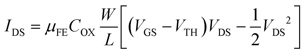 | (1) |
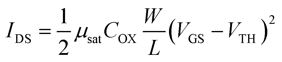 | (2) |
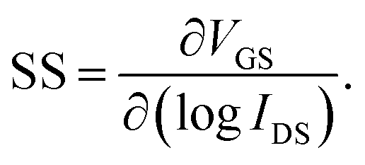 | (3) |
3. Results and discussion
First, the structural characteristics of ZTO thin films with different cation compositions and PDA temperatures were evaluated. Fig. 1(a) shows the GIXRD results of the as-deposited ZnO, SnO2, and ZTO thin films having different Sn concentrations. In the case of the ZnO (Sn 0 at%) thin film, a strong (002) peak was observed at 2θ ∼ 34.4°, suggesting the crystallization of the film with the wurtzite structure. In the case of the Sn 16 at% sample, a weak crystal peak was observed at 2θ ∼ 33.3°, which could also be assigned to the wurtzite (002) plane with a slightly larger interplanar spacing due to the incorporation of Sn, which has a larger atomic radius than Zn. The thin films with a composition ratio of Sn >20 at% had an amorphous structure due to the intermixing of ZnO and SnO2. The pure SnO2 film also showed no diffraction peaks suggesting an amorphous structure. Fig. 1(b)–(g) show plane-view SEM images of the ZTO thin films with different Sn concentrations. In the case of the Sn 16 at% (Fig. 1(b)), uniform nanocrystalline grains with an average diameter of ∼10 nm were observed, which was also true for the ZnO film (data not shown). For the films with Sn >20 at% (Fig. 1(c)–(g)), the smooth surface shape was observed with no grain shapes, which corroborates the GIXRD results. Pure SnO2 film showed a similarly smooth surface (data not shown).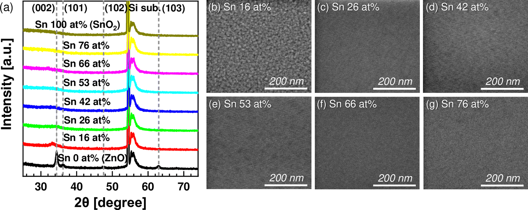 | ||
| Fig. 1 (a) GIXRD patterns of ZnO, SnO2, and ZTO films with different Sn concentrations (as deposited). Planar SEM images of the ZTO films with (b) Sn 16 at%, (c) Sn 26 at%, (d) Sn 42 at%, (e) Sn 53 at%, (f) Sn 66 at%, (g) Sn 76 at%. | ||
Fig. 2(a)–(f) show the GIXRD results of the ZTO films with Sn concentrations of 16, 26, 42, 53, 66, and 76 at%, respectively, after the PDA at temperatures from 500 to 800 °C. The film with Sn 16 at% (Fig. 2(a)), which was already crystallized in the as-deposited state, showed increasing crystallinity with increasing PDA temperature, inducing evident ZnO and Zn2SnO4 peaks. A similar trend was observed for the 26 at% case but with less crystallization at low PDA temperatures. The films with 42 and 53 Sn at% showed no diffraction peaks up to 600 °C, suggesting high amorphous stability. However, as the PDA temperature increased to 700 °C, the films showed Zn2SnO4 and SnO2 peaks. The Sn 66 at% film showed a similar crystallization temperature of 700 °C, but all the diffraction peaks correspond to SnO2. A similar trend was also observed for the Sn 76 at% film, which showed a lower crystallization temperature of 600 °C.
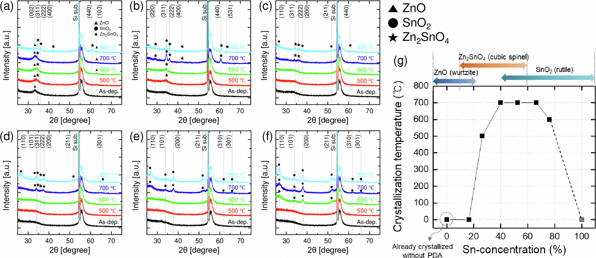 | ||
| Fig. 2 GIXRD patterns of ZTO films with different post-deposition annealing temperatures for 1 hour in air for (a) Sn 16 at%, (b) Sn 26 at%, (c) Sn 42 at%, (d) Sn 53 at%, (e) Sn 66 at%, (f) Sn 76 at%. ZnO, SnO2, and Zn2SnO4 crystal peaks were identified by JCPDS cards (ZnO (no. 01-080-0075), SnO2 (no. 00-041-1445), Zn2SnO4 (no. 00-024-1470)). (g) The crystallization temperature (Tx) of the ZTO films with different Sn concentrations (Tx was determined by the presence of XRD crystal peaks after post-deposition annealing. Tx = 0 °C means that it is already crystallized without annealing after deposition). | ||
Fig. 2(g) summarizes the crystallization trend (crystallization temperature and crystalline phases) of the various ZTO films. Again, these trends are because the different crystallographic arrangements of wurtzite-structured ZnO and rutile-structured SnO2 complicate the overall crystallization process as additional materials are added to each binary material.
Fig. 3(a) shows the variation of the Sn atomic composition ratio (Sn/Zn + Sn) of various ZTO thin films measured by XRF as a function of PDA temperature. In all samples, the Sn atomic composition ratio remained constant (within ±1 at% of the variation) regardless of the PDA temperature. Fig. 3(b) shows the XRR spectrum of the Sn 42 at% film after the different PDA, indicating the density variation. Also, the XRR spectra of all other ZTO films were examined, and the density variations, estimated from the critical angles of the XRR data, are summarized in Fig. 3(c). In this graph, the 0 °C PDA temperature indicates the as-deposited film. For the as-deposited films, the thin film density increased from 6.04 to 6.38 g cm−3 with the increasing Sn concentration due to the higher atomic weight of Sn compared to Zn (Sn 118.71, Zn 65.38).
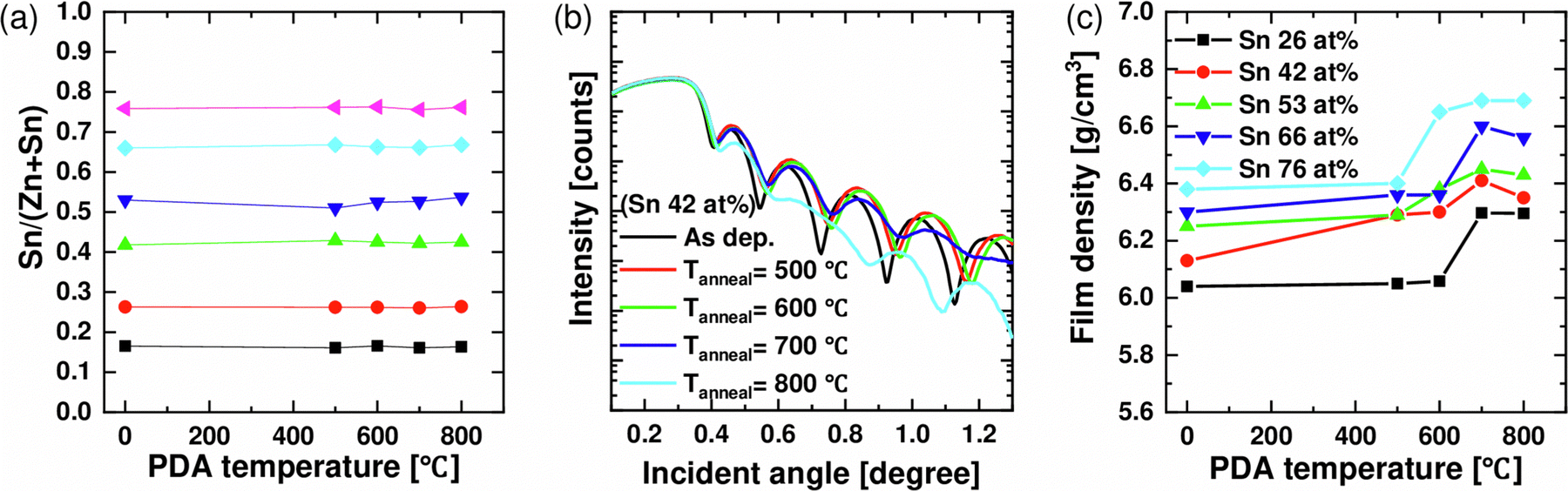 | ||
| Fig. 3 (a) Atomic composition ratio of Sn in ZTO films with different PDA temperatures for 1 hour in the air. (b) Representative XRR spectra of 20 nm-thick ZTO with Sn 42 at% as a function of PDA temperature. (c) Film density as a function of PDA temperature in ZTO films with different Sn concentrations. The film density could be obtained through fitting of the XRR spectra. | ||
For the films with Sn 26, 66, and 76 at%, the film density did not vary up to 500 °C but abruptly increased when they crystallized at 700 or 600 °C. However, for the films with the highest amorphous stability, i.e., Sn 42 and 53 at%, their density gradually increased up to 600 °C and showed the peak value at 700 °C. This behavior may result in promising electrical performance for the amorphous ZTO film, which was indeed the case, as discussed later. The higher density of crystalline ZTO than amorphous ZTO is consistent with the general trend of oxide materials.
It was noted that there was a slight decrease in the film density when the films with Sn compositions of 42%, 53%, and 66% were annealed at 800 °C. This behavior is because these compositions lead the different crystal structures to coexist when they are crystallized. Fig. 2 shows that SnO2 and Zn2SnO4 exist at 42% and 53% Sn composition. As a result, a rough surface may have formed due to the mismatch between the different lattice structures, potentially leading to a decrease in film density, as shown by the AFM images and measured roughness of each concentration (Fig. S1, ESI†).
The degree of densification of thin films is estimated by the ratio of the experimental density of deposited thin films to the theoretical density of crystals. The observed densities for the as-deposited and 800 °C PDA Sn 26 at% sample, in which only a single phase of Zn2SnO4 (cubic spinel, 6.43 g cm−3) was observed (Fig. 2(b)), were 6.04 and 6.30 g cm−3, which correspond to 94.0 and 97.9%, respectively, of Zn2SnO4. Since other films contained wurtzite and rutile phases in addition to the spinel phase, of which the relative portions could hardly be calculated from only the GIXRD, it was challenging to estimate the relative density of the as-deposited and PDA films. Nonetheless, the 94% relative density of the as-deposited film, despite the relatively low ALD temperature (250 °C), is a promising value for the electrical performance. Furthermore, the Auger electron spectroscopy depth profile results of similar films reported elsewhere12 confirmed a carbon impurity level of <1.2 at%, corroborating the high relative density of the as-deposited film. If the as-deposited film had a low relative density, ca. <80%, the PDA might induce severe densification and accompanying stress and even micro-cracking, which could be detrimental to the electrical performance of the channel layer.
Next, the electrical characteristics of the as-deposited ZTO thin film with different Sn concentrations were evaluated. Fig. 4(a) shows the variations in the resistivity (ρ), the electron density (ne), and μHALL obtained from the Hall measurements as a function of the Sn concentration. The Hall pattern was formed using a square-type Van der Pauw configuration. The film with Sn 16 at%, which was already crystallized even in the as-deposited state, was excluded from the Hall measurement. As a result, as the Sn concentration increased, ρ decreased from ∼5 Ω cm to ∼0.003 Ω cm, and ne and μHALL increased from ∼1017 cm−3 and 15.9 cm2 V−1 s−1 to ∼1019 cm−3 and ∼25.9 cm2 V−1 s−1. Fig. 4(b)–(e) show the O 1s XPS results when Sn concentrations are 26, 42, 53, and 66 at%. The O 1s peak consisted of two components: the oxygen bonded with metal ions and the oxygen near oxygen vacancy (VO). As Sn concentration increased, the latter significantly decreased, while the former did not show notable variation. Fig. S2 (ESI†) shows the Zn 2p, Sn 3d, and O 1s XPS peaks of all samples. It was identified that all peaks moved to higher binding energy with similar energy difference (∼0.5 eV) without any shape difference as the Sn concentration increased. These XPS results indicated little change in the chemical bonding nature while the Fermi level (EF) changed (binding energy = hν − Ekin − (Evac − EF)) as the Sn concentration varied.
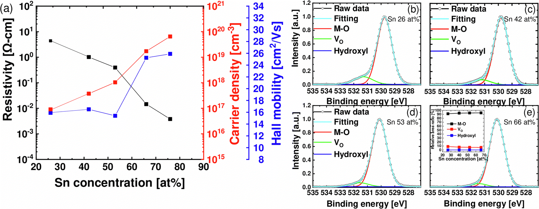 | ||
| Fig. 4 (a) Resistivity, carrier density, and Hall mobility for ZTO films as a function of Sn concentration. XPS O 1s spectra and their deconvolution for the ZTO films with (b) Sn 26 at%, (c) Sn 42 at%, (d) Sn 53 at%, (e) Sn 66 at%. The inset in the panel shows the variation of the relative area ratio calculated from the O 1s spectra as a function of Sn concentration. | ||
Also, μHALL increased as the Sn concentration increased, which is explained by percolation conduction. Generally, carrier conduction in AOS is described as trap-limited and percolation conduction.13 For example, in the accumulation mode of AOS, electrons first fill deep traps at tail states near the conduction band edge (CBE), and then fill shallow traps. In this situation, as the density of electrons increases, conduction through relatively shallower traps occurs, and thus the hopping barrier decreases, and the mobility increases. Lastly, the tendency of decreasing ρ with increased Sn concentration is explained by the increase in ne and μHALL (ρ = 1/qneμHALL).
Fig. 5(a) shows a plan-view SEM image (upper panel) and the schematic diagram (lower panel) of the fabricated ZTO TFTs (as-deposited films). Fig. 5(b) and (c) show IDS–VGS curves when VDS is 0.1 V and 10 V, respectively, corresponding to linear and saturation regions. The output curves of the TFTs with each Sn-concentration are shown in Fig. S3 (ESI†). Fig. 5(d) shows the variations in the VTH, SS, and field effect mobility (μFE) extracted from the corresponding IDS–VGS curve as a function of Sn concentration. As the Sn concentration was increased to 26, 42, and 53 at%, VTH decreased to 0.08, −0.07, and −10.9 V, corroborating the increasing ne shown in Fig. 4(a). For Sn 66 and 76 at%, the transistor was not turned off even under large negative VGS, which could be ascribed to their too-high ne, >1019 cm−3. SS remained at similar values of 0.321 and 0.313 V decade−1 at Sn 26, 42 at% and increased to 0.726 V decade−1 at Sn 53 at%. SS is mainly affected by semiconductor–insulator interface traps (Dit) and GI thickness. In the case of an n-type transistor operating in accumulation mode, it is also greatly affected by tail states near the CBE in the bandgap.14 A recent study9 reported that the localized states locating ∼0.1–0.4 eV deeper than the donor level near the CBE were distributed farther from the CBE, forming long tail states, as the concentration of Sn in an IZO thin film increased. Since the region where localized states are present near the CBE is included in the subthreshold region of the n-type transistor, an increase in these states may cause an increase in SS in ZTO thin films with an Sn concentration of >∼50 at%. As Sn increased to 26, 42, and 53 at%, μFE increased to 4.0, 10.3, and 17.3 cm2 V−1 s−1. It was notable that μFE was similar to μHALL at 53 at%, but μFE was much lower than μHALL for the Sn concentrations of 42 and 26 at%. The most likely cause is the difference in channel length (Lch) on the test pattern: Lch on the TFT pattern for measuring μFE was 5 μm while it was 140 μm in the Hall pattern. While the contact resistance hardly influenced the μHALL, the contact resistance between the channel layer and the S/D electrode (Rsd) substantially influenced the μFE, especially when Lch is short. This effect could be more pronounced when the channel layer has a lower carrier concentration, increasing the contact resistance. Therefore, to confirm the impact of Rsd on μFE, Rsd of ZTO TFTs with different Sn concentrations was evaluated using the transmission line method (TLM).
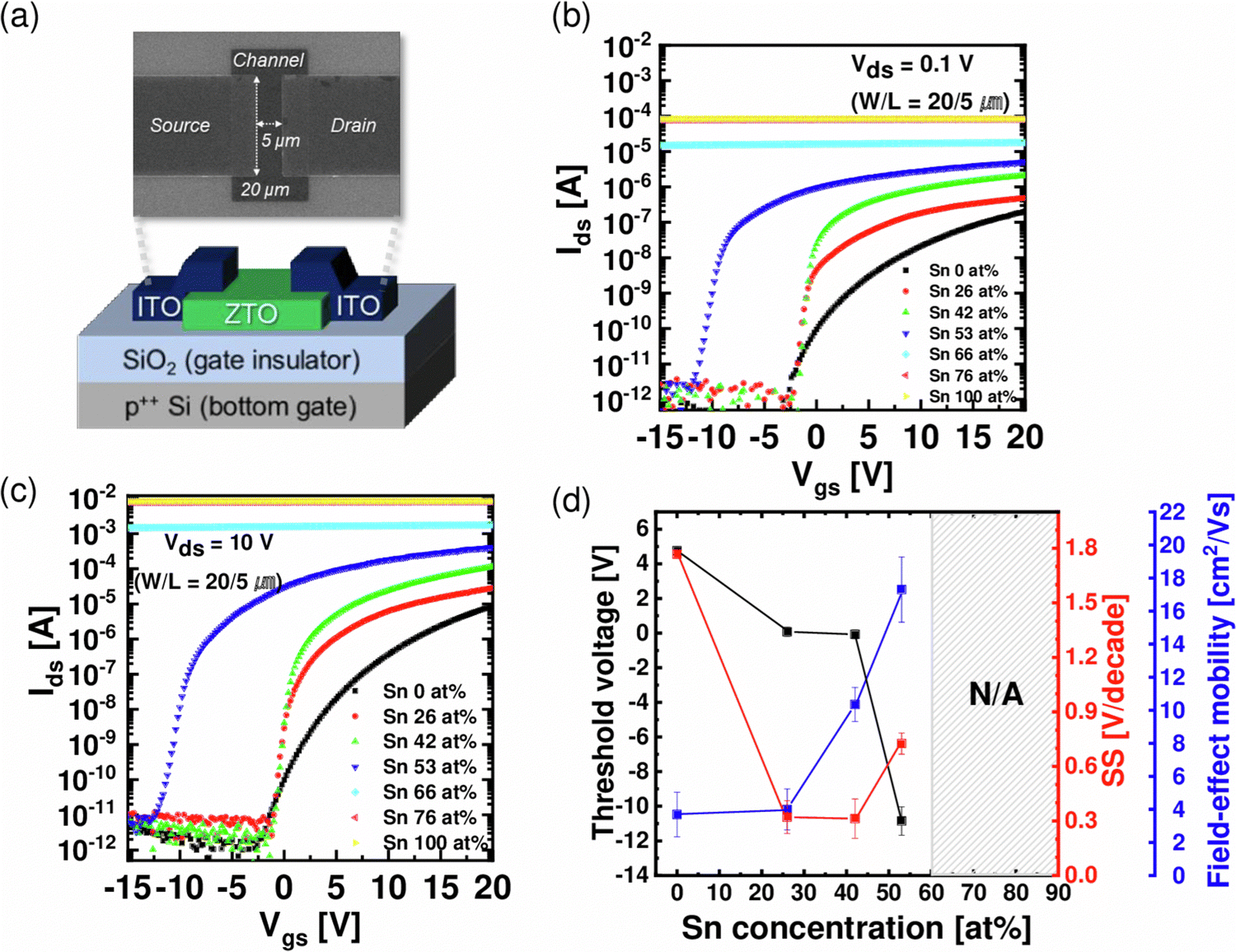 | ||
| Fig. 5 (a) Plan-view and schematic diagram of the inverted staggered-type ZTO TFT, which has a channel width/length of 20/5 μm. The transfer characteristics (Ids–Vgs) of the ZTO TFTs at Vds of (b) 0.1 V in the linear operation region and (c) 10 V in the saturation region with different Sn concentrations. (d) Representative electrical parameters of the ZTO TFTs extracted from transfer characteristics as a function of Sn concentration. Five or more TFTs were measured for each condition. | ||
Fig. 6 shows total resistance (Rtot) extracted through the TLM in Sn 26, 42, 53 at% as a function of the Lch. Sn 66, 76 at% samples were excluded because they could not be turned off. By measuring Rtot using TLM patterns with different Lch, channel resistance (Rch) and Rsd can be calculated through eqn (4), where the slope and y-intercept of the linear fitted lines corresponded to the Rch and Rsd, respectively.
 | (4) |
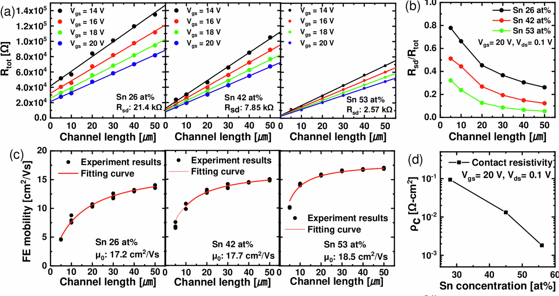 | ||
| Fig. 6 (a) Rtot as a function of the channel length for various gate biases (Vgs) at Vds = 0.1 V for Sn 26 at%, Sn 42 at%, Sn 53 at%. (b) Rsd/Rtot as a function of channel length with different Sn concentrations. (c) The field-effect mobility (μFE) as a function of the channel length for Sn 26 at%, Sn 42 at%, Sn 53 at%. (d) The specific contact resistivity (ρc) as a function of Sn concentration at Vgs = 20 V and Vds = 0.1 V. | ||
First, as VGS increased in each composition, Rsd decreased due to the Schottky barrier lowering effect by the increased carrier concentration at the S/D contact. Second, Rtot and Rsd decreased when the Sn concentration increased from 26 to 53 at%, and, as shown in Fig. 6(b), Rsd/Rtot at the same Lch decreased as the Sn concentration increased. In addition, the specific contact resistivity (ρc) was calculated at VGS = 20 V and VDS = 0.1 V using the relation ρc = RcAc, where Ac is the effective contact area. As a result, as shown in Fig. 6(d), ρc decreased as the Sn concentration increased, which is the reason why the lower the Sn concentration, the lower the μFE in Fig. 5(d). To further verify the effect of Lch on μFE and Rsd, the change in μFE as a function of Lch in each composition was confirmed. As shown in Fig. 6(c), the decrease of μFE was observed as Lch decreased from 50 to 5 μm, and more significant μFE degradation was observed as the Sn concentration decreased from 53 to 26 at%. The results of this experiment can be expressed as the following eqn (5).15 As the Rsd increases, the μFE extracted from the transconductance (gm) decreases from the intrinsic mobility (μ0) of the ZTO thin film.
 | (5) |
By fitting the results of Fig. 6(c) in the above equation, it was confirmed that the extracted μ0 were 17.2, 17.7, and 18.5 cm2 V−1 s−1, similar to μHALL, and Rsd were 11.6, 7.6, and 2.4 kΩ, which were similar to the TLM results. Fig. 6(d) shows the ρc variation with Sn concentration. Therefore, although the μ0 of the ZTO thin films at Sn 26–53 at% had similar values, μFE changed as Rsd/Rtot varied. The difference in Rsd depending on Sn concentration is due to the change in the Schottky barrier height (ϕB = ϕm − χ). In recent studies,16 the electron affinity (χ) increased from 4.05 to 4.45 eV as the Sn concentration increased from 21 to 100 at% in ZTO thin films. Considering the work function (ϕm = 4.67 eV) of ITO used as the S/D electrode, the electron barrier decreased from 0.62 to 0.22 eV, assuming no Fermi level pinning at the S/D electrode interface. Generally, ρc is exponentially proportional to ϕB. When the doping concentration of the semiconductor is higher than 1019 cm−3, the Fowler–Nordheim tunneling can also contribute to electrical conduction.17 Therefore, contact resistance should be decreased to achieve high electrical performance, especially for low Sn-concentration devices. Sn 42 at% film was identified as the preferred sample with the highest amorphous stability and electrical performances from these test results of the as-deposited films. Therefore, the variations of its electrical performance as a function of PDA temperature were further evaluated.
Fig. 7(a) and (b) show the IDS–VGS curves of the films after PDA at 500, 600, 700, and 800 °C, when VDS is 0.1 V and 10 V, respectively. Fig. 7(c) and (d) show the summary of the electrical characteristics extracted from the corresponding IDS–VGS curve as a function of PDA temperature. The electrical properties improved up to 600 °C, where crystallization was not observed. Gate leakage increase, which can occur due to the reaction between the ZTO film and SiO2 during high-temperature annealing, was not observed under any PDA conditions. μFE increased from 10.3 to 25.5 cm2 V−1 s−1, while VTH (∼0 V) and SS (∼0.30 V decade−1) did not show a notable change. The SS of ∼0.30 V decade−1 is not sufficiently low to be considered a channel material for 3D DRAM. However, this high SS value is mainly ascribed to the thick (100 nm) SiO2 GI thickness. As shown in Fig. 3(d), the film density increased at 600 °C, which may decrease the probability of electrons being trapped or scattered. Also, as the density of the ZTO thin film increased, the overlap of the ns orbital, which is the electron transfer path of the oxide semiconductor, increased, enhancing mobility. However, after the PDA at 700 and 800 °C, in which the film was crystallized, the VTH and SS increased rapidly, and μFE decayed significantly. These results suggest that the grain-boundary-related defect increased as the ZTO thin film crystallized, and thus the carrier scattering increased. Therefore, the TFT process temperature should not go over 600 °C.
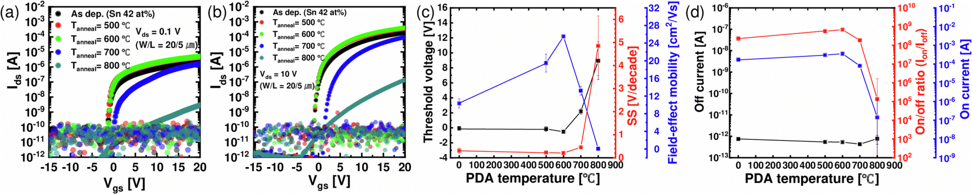 | ||
| Fig. 7 Transfer characteristics (IDS–VGS) of the ZTO TFTs (Sn 42 at%) at Vds of (a) 0.1 V and (b) 10 V with different PDA temperatures, accompanied by transparent dots meaning gate current. (c) Representative electrical parameters and (d) on/off current characteristics of the ZTO TFTs as a function of PDA temperature. | ||
Finally, the possible reasons for the VTH variation with the Sn-concentration variation are discussed below. The two factors that possibly change the EF and ne are (i) the density of VO and (ii) the shallow donor energy (ED). First, it is known that the ne of an oxide semiconductor is generally determined by VO concentration, and one VO may provide the conduction band with a maximum of two free electrons.18 Second, ED determines the activation of the VO, and, thus, the carrier concentration in the conduction band. According to density functional theory calculations, the defect level caused by VO in SnO2 was closer to the conduction band edge (CBM) by ∼1 eV than in ZnO.19 Additionally, a report on metal–organic chemical vapor deposited ZTO films revealed that the energy state of Sn-related oxygen vacancies was approximately 0.2 eV closer to the CBM than that of Zn-related oxygen vacancies.20
The results of the TCAD simulation using Silvaco ATLAS based on the subgap state distribution shown in Fig. 8(a) confirmed these speculations. Specific parameters and formulas for calculating the transfer curves are summarized in Tables S1 and S2 (ESI†). The transfer curve of the Sn 42 at% TFT was used as the reference condition for the simulation. Fig. 8(b) shows the coincident measured (black line) and simulated (red line) transfer curves of Sn 42 at% TFT, suggesting the accuracy of the simulation. Fig. 8(c) confirmed that as the total number of Gaussian donor states (ngd) among the subgap states increased, VTH shifted negatively, and Ion increased slightly. However, the XPS analysis in Fig. 4 showed that the VO concentration decreases (ngd decreases) with increasing Sn-concentration. In contrast, the VTH of the TFT decreases, as shown in Fig. 8. Therefore, ngd variation cannot explain the VTH variation according to the Sn concentration.
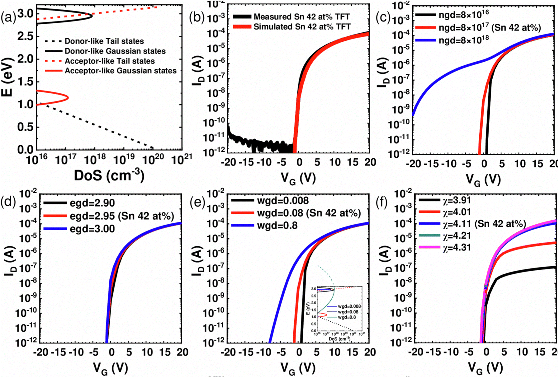 | ||
| Fig. 8 (a) Fitted electronic structure of a-ZTO with formulas of the density of states. Specific model parameters and formulas are shown in Tables S1 and S2 (ESI†). (b) Measured and simulated transfer curve of Sn 42 at% TFT, simulated by technology computer-aided design (TCAD). Simulated transfer curves depending on (c) total density of Gaussian donor-like states (ngd), (d) peak energy level of Gaussian donor-like states (ED, egd), (e) characteristic decay energy of Gaussian donor-like states (wgd) with an inset of the distribution of subgap states and (f) electron affinity of simulated channel. | ||
Besides, the location of the shallow donor states (egd) did not significantly affect the transfer curves, as shown in Fig. 8(d). This finding is due to the shallow nature of all the assumed shallow donor levels. Instead, Fig. 8(e) shows that the characteristic decay energy of the shallow donor states (wgd) significantly impacts the transfer curve. As the wgd increases, the shallow donor state spreads widely, and the ratio of states existing above the CBM increases, causing the EF to be closer to the CBM and VTH to shift negatively. Therefore, it can be inferred that as the Sn composition ratio increases, the wgd increases due to the metastable Sn–O bonding nature compared with the Zn–O bonding. This effect may increase the proportion of shallow donor states located over the CBM, leading to an increase in intrinsic ne and channel conductivity, despite the decrease in total VO concentration.
Besides, the electrical contact properties between the ZTO channel and source/drain electrodes might also affect the electrical performance. As shown in Fig. 6(b), these contact properties significantly contributed to the TFT device's total resistance, although the channel length (5–50 μm) is relatively long. The source and drain contact properties are governed by the Schottky barrier at the junction, which is controlled by the electron affinity of the ZTO channel, depending on the Zn/Sn ratio, for the given contact metal (ITO). Therefore, the transfer curves are simulated with different electron affinities of the ZTO channel, as shown in Fig. 8(f). However, this parameter did not influence the VTH value but did most notably the on-current.
4. Conclusions
In this study, the crystallization behaviors and the electrical characteristics of ALD ZTO thin films, depending on the ratio of zinc and tin, were carefully examined. When the Sn concentration was lower than 16 at%, the as-deposited film was already crystallized with the wurtzite structure, while other films with higher Sn concentration remained amorphous. It was confirmed that the crystallization temperature of the ZTO thin film was the highest (∼700 °C) at Sn 42–66 at% where the different crystallographic structures of ZnO (wurtzite) and SnO2 (rutile) suppressed the ordering of the constituent elements. In addition, as the Sn-concentration increases, ne and μHALL increase, and ρ decreases. As a result of further analysis of electrical properties by manufacturing TFTs, SS was optimized at 26 to 42 at% under the influence of tail states near the CBE. μFE showed different trends to μHALL depending on composition ratio: Sn 26, 42, 53 at%, μFE = 4.0, 10.3, 17.3 cm2 V−1 s−1, μHALL = 15.9, 16.5, 15.4 cm2 V−1 s−1, respectively. Such a difference was attributed to the increased source and drain contact resistance when the Sn concentration was low. When the contact resistance components were excluded, the channel carrier mobility was commonly 17–18 cm2 V−1 s−1 for the three Sn concentrations, consistent with the μHALL values.The electrical characteristics of 42 at% ZTO thin films, the optimized composition based on an as-deposited sample, were analyzed depending on the PDA temperature. As a result, mobility increased up to 600 °C due to the decrease in trapping and scattering of electrons due to densification while keeping the amorphous structure. The achieved VTH, μFE, and SS were −0.52 V, 25.5 cm2 V−1 s−1, and 0.30 V decade−1, respectively. The μFE is highly promising for 3D DRAM applications. The VTH and SS values need improvements, which could be acquired by work function control of the gate metal and GI thickness decrease. However, the PDA at temperatures higher than 700 °C severely degraded the device performance, which could be ascribed to the adverse crystallization of the ZTO films. Therefore, the entire integration process should not involve temperatures higher than 600–700 °C.
Finally, to confirm the specific reason for the dependence of the electrical properties on the Sn-concentration, ZTO TFT devices with various channel conditions were simulated by TCAD simulation. The simulation showed that the increase in the distribution of shallow donor states decreases VTH, and higher electron affinity increases Ion.
Conflicts of interest
There are no conflicts to declare.Acknowledgements
This work was supported by the next-generation Intelligence Semiconductor Foundation (NIS2030, grant number 2022M3F3A2A01079620).References
- D. Ha and H.-S. Kim, 2022 IEEE Symposium on VLSI Technology and Circuits (VLSI Technology and Circuits), 2022, pp. 417–418 Search PubMed.
- A. Belmonte, H. Oh, N. Rassoul, G. L. Donadio, J. Mitard, H. Dekkers, R. Delhougne, S. Subhechha, A. Chasin, M. J. van Setten, L. Kljucar, M. Mao, H. Puliyalil, M. Park, L. Teugels, D. Tsvetanova, K. Banerjee, L. Souriau, Z. Tokei, L. Goux and G. S. Kar, 2020 IEEE International Electron Devices Meeting (IEDM), 2020, pp. 28.2.1–28.2.4 Search PubMed.
- J. K. Park, S.-Y. Kim, K.-H. Lee, S. H. Pyi, S.-H. Lee and B. J. Cho, 2014 Symposium on VLSI Technology (VLSI-Technology): Digest of Technical Papers, 2014, pp. 1–2 Search PubMed.
- R. Degraeve, S. Clima, V. Putcha, B. Kaczer, P. Roussel, D. Linten, G. Groeseneken, A. Arreghini, M. Karner, C. Kernstock, Z. Stanojevic, G. Van den bosch, J. Van Houdt, A. Furnemont and A. Thean, 2015 IEEE International Electron Devices Meeting (IEDM), 2015, pp. 5.6.1–5.6.4 Search PubMed.
- K. Nomura, H. Ohta, A. Takagi, T. Kamiya, M. Hirano and H. Hosono, Nature, 2004, 432, 488–492 CrossRef CAS PubMed.
- Y. Kobayashi, S. Matsuda, D. Matsubayashi, H. Suzawa, M. Sakakura, K. Hanaoka, Y. Okazaki, T. Yamamoto, S. Hondo, T. Hamada, S. Sasagawa, M. Nagai, Y. Hata, T. Maruyama, Y. Yamamoto and S. Yamazaki, Jpn. J. Appl. Phys., 2014, 53, 04EF03 CrossRef.
- T. Kamiya, K. Nomura and H. Hosono, Sci. Technol. Adv. Mater., 2010, 11, 044305 CrossRef PubMed.
- J. Sheng, H.-J. Lee, S. Oh and J.-S. Park, ACS Appl. Mater. Interfaces, 2016, 8, 33821–33828 CrossRef CAS PubMed.
- J. Sheng, T. Hong, D. Kang, Y. Yi, J. H. Lim and J.-S. Park, ACS Appl. Mater. Interfaces, 2019, 11, 12683–12692 CrossRef CAS PubMed.
- C. Granqvist and A. Hultåker, Thin Solid Films, 2002, 411, 1–5 CrossRef CAS.
- J. Heo, S. B. Kim and R. G. Gordon, Appl. Phys. Lett., 2012, 101, 113507 CrossRef.
- J. S. Kim, Y. Jang, S. Kang, Y. Lee, K. Kim, W. Kim, W. Lee and C. S. Hwang, J. Phys. Chem. C, 2020, 124, 26780–26792 CrossRef CAS.
- S. Lee, K. Ghaffarzadeh, A. Nathan, J. Robertson, S. Jeon, C. Kim, I.-H. Song and U.-I. Chung, Appl. Phys. Lett., 2011, 98, 203508 CrossRef.
- M. Kimura, T. Nakanishi, K. Nomura, T. Kamiya and H. Hosono, Appl. Phys. Lett., 2008, 92, 133512 CrossRef.
- K.-Y. Chan, E. Bunte, H. Stiebig and D. Knipp, Appl. Phys. Lett., 2006, 89, 203509 CrossRef.
- S. Lee, S. Kim, S. Shin, Z. Jin and Y.-S. Min, J. Ind. Eng. Chem., 2018, 58, 328–333 CrossRef CAS.
- D. Schroder, Semiconductor Material and Device Characterization, Wiley, 2015 Search PubMed.
- T. Kamiya and H. Hosono, NPG Asia Mater., 2010, 2, 15–22 CrossRef.
- P. Ágoston, K. Albe, R. M. Nieminen and M. J. Puska, Phys. Rev. Lett., 2009, 103, 245501 CrossRef PubMed.
- U. K. Kim, S. H. Rha, J. Hwan Kim, Y. J. Chung, J. Jung, E. S. Hwang, J. Lee, T. J. Park, J.-H. Choi and C. S. Hwang, J. Mater. Chem. C, 2013, 1, 6695–6702 RSC.
Footnotes |
| † Electronic supplementary information (ESI) available. See DOI: https://doi.org/10.1039/d2tc05090k |
| ‡ W. Kim and S. Kang contributed equally to this work. |
| This journal is © The Royal Society of Chemistry 2023 |