
 Open Access Article
 This Open Access Article is licensed under a
 Creative Commons Attribution 3.0 Unported Licence
Graphene memristors based on humidity-mediated reduction of graphene oxide†
Fatemeh
Haghshenas Gorgabi
 a,
Maria C.
Morant-Miñana
b,
Haniyeh
Zafarkish
a,
Davood
Abbaszadeh
*a and
Kamal
Asadi
*c
a,
Maria C.
Morant-Miñana
b,
Haniyeh
Zafarkish
a,
Davood
Abbaszadeh
*a and
Kamal
Asadi
*c
aPhysics Department, Institute for Advanced Studies in Basic Sciences, Zanjan 45137-66731, Iran. E-mail: d.abbaszadeh@iasbs.ac.ir
bCentre for Cooperative Research on Alternative Energies (CIC energiGUNE), Basque Research and Technology Alliance (BRTA), Alava Technology Park, Albert Einstein 48, Vitoria-Gasteiz 01510, Spain
cDepartment of Physics, University of Bath, Claverton Down, Bath BA2 7AY, UK. E-mail: ka787@bath.ac.uk
First published on 16th January 2023
Abstract
Memristors have emerged as promising devices for neuromorphic applications, particularly as synaptic weight. Graphene oxide, a partially oxidised and electrically insulating form of graphene, has been employed in metal/insulator/metal devices, where resistance switching based on the filamentary growth of the contacting metals has been demonstrated. Here we demonstrate an alternative highly reproducible resistance switching mechanism based on solid-state reduction of GO thin-films mediated by adsorbed water. It is shown that distinguishable and highly stable resistance states can be controllably realised in graphene oxide metal/insulator/metal devices. We have unravelled the growth mechanism and determined the growth kinetic of reduced graphene oxide, which enables a deterministic way to tune the resistance in GO devices. The demonstration of highly reproducible memristors based on graphene oxide crossbar devices is very promising for the realisation of low-cost and environmentally benign solution-processable neuromorphic synaptic weight.
Introduction
Resistance switching (RS) devices, particularly memristors, have gained considerable attention for application in neuromorphic computing. Memristors are two-terminal metal/insulator/metal (MIM) devices that exhibit reversible resistance switching from a high resistance state (HRS) through intermediate resistance states to a low resistance state (LRS) upon applying a voltage. Accessibility of the intermediate states and their stability render memristors ideal candidates for neuromorphic applications, particularly as synaptic weight.Graphene oxide (GO) is a partially oxidised form of graphene that is produced on a large scale using low-cost methods such as liquid-phase exfoliation in the presence of oxidising agents. Various oxygen-containing functional groups on the surface render GO dispersible in water. Dispersibility in water enables solution processing of GO thin films that can be used in microelectronic applications.1 GO or its reduced form, i.e. reduced graphene oxide (rGO), has been successfully used for solution-processable devices2 such as field-effect transistors,3,4 solar cells,5 and supercapacitors as transparent conductive films,6 and electrically controlled water permeation.7
GO memristor devices have been recently reported8–10 and proposed for application as synaptic weights in neuromorphic devices.11,12 The GO memristors, typically fabricated by sandwiching a thin GO layer between two metallic electrodes, show gradual and abrupt transitions from HRS to LRS. The measurements are usually performed by applying a bias, typically ≥|4 V|, to perform the set and reset process. The voltage at which resistance transition occurs is usually stochastic and not well-defined. The proposed switching mechanism for resistance switching is based on the filamentary growth of the contacting metals through the graphene layer.8,11 For many of the envisioned applications, the operation of the device in ambient conditions is desired, where it has been shown that the presence of ambient humidity causes electrochemical reduction of GO due to electrolysis of the ambient water.13–16
Here we demonstrate a well-controlled humidity-mediated resistance-switching process in GO thin-film memristors. It is shown that distinguishable and highly stable resistance states can be controllably realised for devices operating in ambient conditions (room temperature ∼23 °C and humidity ∼45%). The change in the resistance is due to the formation of highly conductive reduced graphene oxide (rGO) dendrites that grow gradually from the cathode to the anode of the GO memristor. The high reproducibility of the reduction mechanism enables establishing of a predictive growth model and estimating the growth dynamic of rGO dendrites. The demonstration of highly reproducible memristors based on GO MIM devices is very promising for the realisation of low-cost and environmentally benign solution-processable neuromorphic synaptic weight.
Results and discussion
Resistance switching in GO crossbar devices
First, a voltage sweep of 0 to 3.5 V and back to 0 is performed on a fresh, pristine GO thin film. We note that throughout of the manuscript unipolar voltage sweeps were used unless otherwise stated (please see Fig. S1 in the ESI† and the relevant discussion). The first current–voltage (I–V) sweep obtained at a voltage sweep rate of 100 mV s−1,given in Fig. 1a as black symbols, shows that the current passing through the GO film steadily increases from 0 to about ∼1 mA as the voltage increased from 0 to about 2.7 V. As the applied voltage increases beyond 2.7 V, the current shows an abrupt jump to 20 mA and increases further as the voltage reaches 3.5 V. Upon the backward voltage sweep, the current remains high and shows a weak nonlinearity with voltage as the voltage is reduced. The hysteretic I–V curve resembles the quasi-rectangular shape of the cyclic voltammetry curve of GO, indicative of a capacitive behaviour typical of an electrical double-layer. This increased conductivity of the GO layer and the shape of the I–V curve indicates the complete reduction of the GO film at voltages above 2.7 V. Upon scanning back, the current remained high, which indicates that the formation of rGO is an irreversible process.17,18 The second I–V sweep in Fig. 1a, red symbols, confirms the successful formation of rGO, as shall be demonstrated later in the manuscript.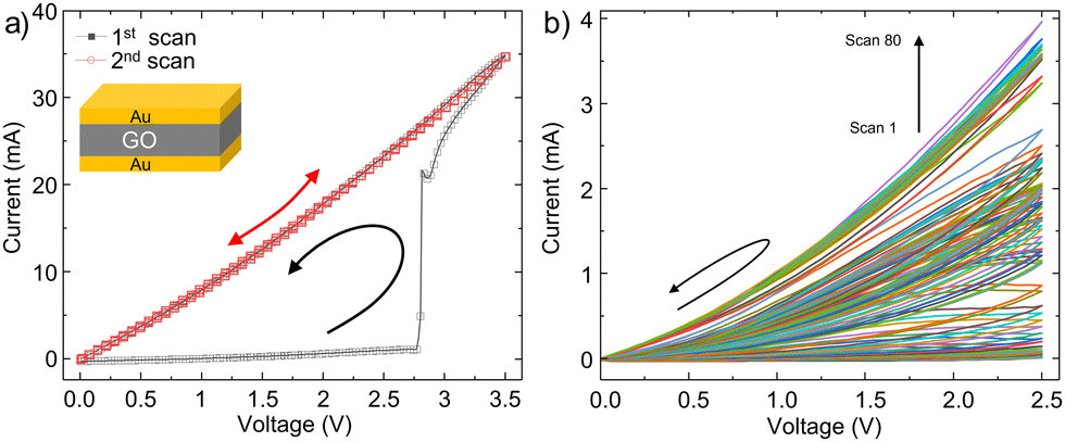 | ||
| Fig. 1 (a) Current–voltage characteristics of GO crossbar devices (scan rate of 100 mV s−1). (b) The evolution of the current-voltage characteristics of a GO device after 80 consecutive scans with a scan rate of 100 mV s−1. The arrows indicate the direction of the current hysteresis. | ||
For the envisioned application as synaptic weight, it is necessary to reproducibly tune the resistance of the GO memristors to any desired time-invariant resistance states between the LRS and HRS. To do so, a series of I–V sweeps with a voltage scan rate of 100 mV s−1 are performed wherein the maximum scan voltage is set to 2.5 V, which is below the onset of the uncontrolled complete reduction, which is at 2.7 V. Fig. 1b shows the resulting I–V curves for 80 consecutive scans. Interestingly, the current passing through the device gradually increases as the number of scans increases, which is indicative of the plasticity behaviour of the GO devices.
The intermediate resistane states are interrogated at 1 V, which is substantially below the programming voltage of 2.5 V, to avoid changes in the resistance of the GO layer due to the reading process. Fig. 2a shows the changes in current against the number of scan cycles. As the cycle number increases, the device current gradually increases. As the number of cycles approaches 60, the current shows a big jump and then stabilises for higher cycle numbers. The gradual increase in current can be attributed to the gradual reduction of the GO layer, and the jump in current can be attributed to the complete reduction of the GO layer.
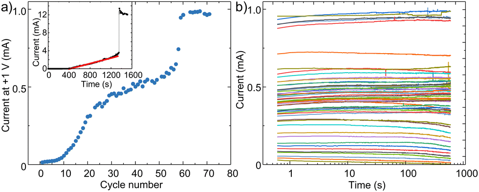 | ||
| Fig. 2 (a) Gradual conductance switching as a function of voltage cycles from 0 V to 2.5 V and back. Inset: Evolution of current in time at a constant bias of 2.5 V. (b) Retention time of the programmed intermediate resistance states. | ||
The current is measured in time to monitor the stability of different intermediate states. After every repeating cycle of 0 to 2.5 V, a small voltage of 1 V is applied to the device, and the current evolution in time is monitored for 10 minutes. Fig. 2b shows that intermediate resistance states are highly stable in time. In the next step, we elucidate the reduction mechanism in GO devices to gain a better understanding of the switching mechanism.
It should be noted that changes in resistance can also be achieved by applying a constant voltage bias of 2.5 over the GO MIM devices. The inset in Fig. 2a shows the current evolution when a constant bias of 2.5 V is applied for about 25 minutes. After a waiting time of ∼400 seconds, the resistance of the device begins to change linearly in time with a slope of 3.0 ± 0.4 μA s−1. After 1250 seconds, the current shows a big jump due to complete reduction of the GO layer as shall be explained in the next section. The linear behaviour is highly reproducible. Similar measurements are performed on numerous fresh GO devices to obtain a reliable statistic. An average waiting time of 353 ± 46 s and gradient of 5.5 ± 2.2 μA s−1 have been obtained. The time at which a sharp transition in current occurs highly depends on the thickness of the GO layer, as shall be discussed in the next section.
Resistance switching mechanism
Elucidating the reduction mechanism in crossbar devices is relatively challenging because the MIM device consists of a thin layer of GO, which is capped by a metallic layer. Therefore, devices with co-planar electrode configurations are employed.19Because the graphene oxide between the two Au electrodes is exposed, it is, therefore, easier to physically and chemically study the resistance-switching mechanism. Fig. 3a shows in-that in-plane GO devices show resistance switching behaviour comparable to the devices with stacked layer configuration as presented in Fig. 1a. Note both devices are measured under the same ambient conditions and voltage scan rate. Hence, the resistance-switching mechanisms in both structures are the same and the in-plane devices can serve as a platform to study the switching mechanism.
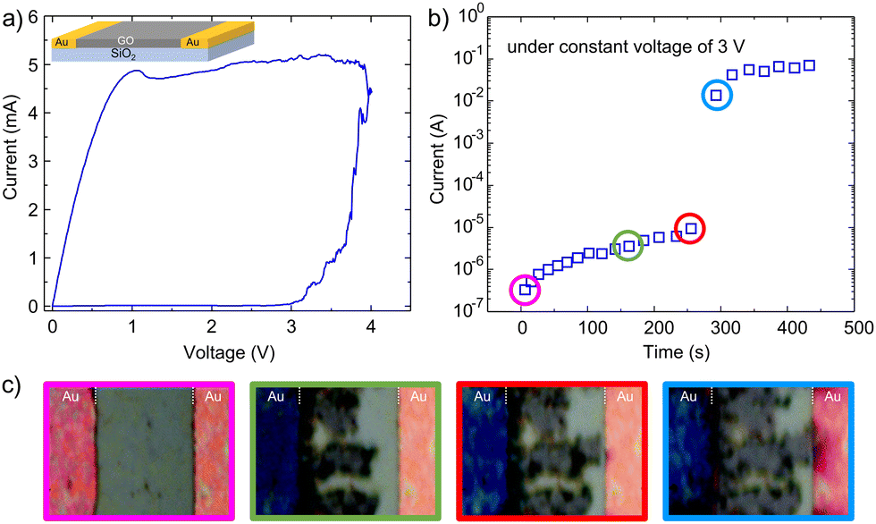 | ||
| Fig. 3 (a) Current–voltage characteristics of an in-plane Au/GO/Au memristor obtained from cyclic voltammetry at a scan rate of 100 mV s−1. The inset shows the schematic of the device. (b) Gradual change of current at a constant bias of 3 V. (c) Real-time optical images of the GO thin-film at different times as indicated with coloured circles in part (b). All the DC electrical measurements were performed using a four-point probe configuration. The measurements are performed at an ambient temperature of 23 °C and relative humidity of 45%. | ||
In the next step, a constant voltage of 3 V is applied to a fresh in-plane device, and the change in current is monitored over time. The device is placed under an optical microscope during the electrical measurement, and the changes in the GO are photographed over time. The plot indicating changes in current is given in Fig. 3b. The current show similar behaviour as discussed in Fig. 2a (inset). Fig. 3c shows the corresponding optical images of the device at the indicated times (coloured circles in Fig. 3b). The GO layer shows a uniform contrast at the early stages of the measurement. However, as time elapses, the contrast of the GO film deposited on the grounded counter electrode changes and dendritic structures emerge at the edge of the grounded electrode. The dendrites grow in time.
The dendrites’ growth is unidirectional from the grounded electrode towards the biased electrode. When a dendrite bridges between the two electrodes, the current substantially increases. The growth of the dendrite continues until the complete GO film covering between the two electrodes is converted.
Raman spectroscopy and X-ray photoelectron spectroscopy (XPS) are performed to determine the chemical nature of the dendrites. Raman spectra of an intact GO layer and a spot on the dendrites are given in Fig. 4a. The spectra are recorded for the dendrite and the unaffected GO part of the film. The green spectrum measured on GO exhibits three main characteristic peaks; the intensity ratio of D- to G-modes, ID/IG = 0.84, which is close to 1 and is indicative of high structural disorder due to the random distribution of regions with oxygen-containing functional groups. In contrast, the Raman spectrum of the dendritic region, the red spectrum, shows a relative increase in the intensity of the D-mode, with ID/IG = 1.54. The increased ratio is the characteristic of a high-density defect regime and reflects a relative increase of sp2 domains.20,21 The Raman spectra unambigeously indicate that the dendrites consist of rGO.
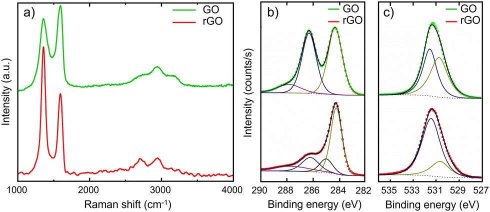 | ||
| Fig. 4 (a) Normalized Raman spectra measured on pristine GO (green) and the rGO dendrites (red). (b) and (c) XPS survey and the corresponding deconvolutions of GO and rGO peaks, where (b) is the high-resolution spectra for C 1s and (c) is the high-resolution spectra for O 1s. | ||
To quantify the extent of the reduction, XPS has been performed on the pristine GO films before the application of a bias and on the rGO film formed by the application of +4 V in co-planar devices. High-resolution XPS survey and the corresponding deconvolutions of C 1s and O 1s peaks for the pristine GO and rGO films are presented in Fig. 4b and c. For the rGO device, the relative intensity of O 1s photoemission with respect to C 1s is reduced as compared to the device with pristine GO. The C 1s spectrum of GO can be deconvoluted into three peaks centred at 284.2, 286.2 and 287.8 eV that corresponds to C sp2, a combination of C–O and C![[double bond, length as m-dash]](https://www.rsc.org/images/entities/char_e001.gif) O, and COO species, respectively.22–24 Interestingly, the deconvoluted spectrum of rGO is dominated by the emission peak from C sp2, and the contribution of C–O, CO and COO bonds is substantially reduced. We note that a fourth peak corresponding to C–C sp3 bonds, centred at 285 eV, needs to be introduced to reconstruct the experimentally measured rGO spectrum. The O 1s spectrum of GO can be deconvoluted into two peaks assigned to COO bonds and to O atoms directly bonded to carbon C–O, which are centred at 530.7 eV and 531.5 eV, respectively.25–27 It should be noted that the species related to OH or O bonded to aromatic C, appearing at binding energies above 533 eV,28 cannot be excluded. However, the components for these species are weak and superimposed by a much stronger peak at 531.5 eV. The O from absorbed water (>534 eV) has not been detected because the water species evaporate under XPS’ ultra-high vacuum condition.29 In agreement with the C 1s spectra, the O 1s spectrum of rGO is dominated by the reduced C–O peak. XPS, therefore, confirms the reduction of GO and restoration of sp2 C–C bonds and thereby increasing the conductivity of the film.
O, and COO species, respectively.22–24 Interestingly, the deconvoluted spectrum of rGO is dominated by the emission peak from C sp2, and the contribution of C–O, CO and COO bonds is substantially reduced. We note that a fourth peak corresponding to C–C sp3 bonds, centred at 285 eV, needs to be introduced to reconstruct the experimentally measured rGO spectrum. The O 1s spectrum of GO can be deconvoluted into two peaks assigned to COO bonds and to O atoms directly bonded to carbon C–O, which are centred at 530.7 eV and 531.5 eV, respectively.25–27 It should be noted that the species related to OH or O bonded to aromatic C, appearing at binding energies above 533 eV,28 cannot be excluded. However, the components for these species are weak and superimposed by a much stronger peak at 531.5 eV. The O from absorbed water (>534 eV) has not been detected because the water species evaporate under XPS’ ultra-high vacuum condition.29 In agreement with the C 1s spectra, the O 1s spectrum of rGO is dominated by the reduced C–O peak. XPS, therefore, confirms the reduction of GO and restoration of sp2 C–C bonds and thereby increasing the conductivity of the film.
The switching mechanism is attributed to the electrolysis of water in the GO layer. In a conventional electrochemical cell, water electrolysis takes place at an electrode potential of 1.26 V. Considering the obtained I–V characteristics of the GO MIM devices, it can be argued that the overpotential in Au/GO/Au devices is about 2 V. The observed overpotential is in good agreement with previous experimental reports30 and the predictions from DFT calculations for the electrolysis on ideal polarisable electrodes such as Au.31,32 It has been suggested that the reduction follows a two-step mechanism summarised as follows: First oxidation of water at the biased electrode takes place:
| 2H2O ⇆ 4H+ + O2 + 4e− | (1) |
| aH+ + be− + GO ⇆ rGO + cH2O | (2) |
Growth kinetic of rGO
The oxidation of water is the rate-determining step in the reduction process and the growth of rGO dendrites. Understanding the growth kinetic is challenging because of the strong dependence of water oxidation on ambient conditions, namely temperature and humidity. Nevertheless, at a fixed temperature and humidity, as done here, it is possible to estimate the growth kinetics. GO is an insulator with relatively low conductance. Hence the potential drop over the GO layer between the metal electrodes in the Au/GO/Au electrodes can be assumed linear. Close to the grounded electrode, the potential drop is largest and large enough to reduce GO. At the same time, the remainder of the GO film remains insulating and highly resistive. The potential drop over the remaining GO layer stays linear because rGO is a good electrical conductor, and the potential drop over the formed rGO can be disregarded. Consequently, the potential between the working electrode and the rGO front varies linearly, and the reduction process continues at the boundary between GO and rGO. Consequently, that the growth of rGO dendrites proceeds one-dimensionally in a front from the grounded electrode to the biased electrode.To estimate the growth speed, we have performed resistance switching measurements for in-plane devices with various electrode spacing. A fixed bias of 3 V is applied to all devices and the time at which a sharp increase in current passing through the device occurs is recorded. The results, given in Fig. 5, show that there is a linear relationship between the reduction time and electrode spacing. The gradient of the linear fit through the data is 5.1 ± 0.6 nm s−1 and indicates the growth speed of the rGO dendritic front. The growth speed highly depends on the experimental conditions, namely ambient humidity and temperature. Hence variation in growth speed at different temperatures, humidity and bias is expected (see Fig. S2 and S3, ESI†). As a final note, the determination of the growth speed is highly beneficial to achieve good control over the resistance change in GO memristors, as it enables a deterministic approach to resistance change in the GO memristors when the thickness of the GO in the MIM device is known.
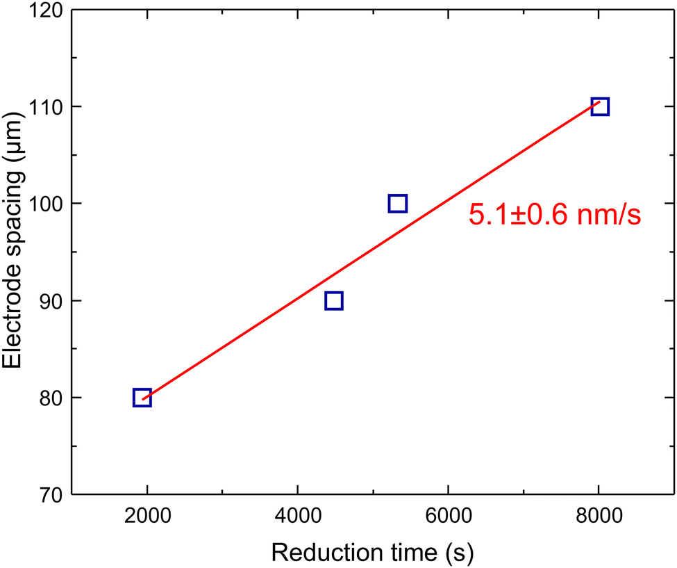 | ||
| Fig. 5 Estimation of the growth velocity of the rGO dendrites by varying the electrode spacing and recording the reduction time. The applied voltage is constant at 3 V, and the room temperature and humidity are 23 °C and ∼40%, respectively. | ||
Experimental
Device preparation: GO was synthesised using Hummers’ method33 and purified as reported in the literature.34 Subsequently, water dispersions of GO with a concentration of 4 mg ml−1 were prepared and used for device fabrication. Homogeneous dispersions are obtained by solution sonication for 1 hour in a 40 kHz ultrasonic bath. Two different sets of GO devices were prepared to test resistance switching. The first set consisted of crossbar devices composed of a stack of Au/GO/Au layers that were prepared on glass substrates. The substrates were cleaned using acetone and, subsequently, ethanol in an ultrasonic bath for 5 minutes. To promote the wettability of the substrates, the surface was treated with UV/O3 plasma for 30 min. Au (20 nm) bottom contact was evaporated through a shadow mask using 1 nm Cr as an adhesion promoter. After drop coating the GO layer and subsequent drying, the memristors were finished by depositing a second Au counter electrode. The second set of devices consisted of a co-planar configuration of Au electrodes. The Au electrodes (50 nm, with 2 nm of Ti as an adhesion layer) were realised photolithographically on silicon monitor wafers with a thermally grown SiO2 layer (200 nm) or on glass substrates using the shadow mask technique. The wafers were thoroughly cleaned using acetone and, subsequently, an ethanol ultrasonic bath for 5 minutes prior to use. Test structures comprised parallel co-planar electrode configurations and were realised using conventional photolithography. The spacing, L, between the Au electrodes was fixed at 50 μm.GO thin films were formed by drop coating from a homogeneous water dispersion on the substrates, followed by a drying step in a vacuum of 0.1 mbar. The GO film thickness was typically between 2 to 5 μm.
Analytical characterisation: Optical images were taken using an optical microscope in reflection mode. Raman spectroscopy was conducted using a Bruker RFS 100/S spectrometer (laser wavelength of 532 nm). The Raman spectra were normalised to the intensity of the 2D peak (2700 cm−1) after the baseline correction. X-Ray photoelectron spectroscopy (XPS) was performed using Kα excitation of an Al source with a photon energy of 1487 eV (Kratos Axis UltraDLD). The measurements were performed using a spot size of 300 × 700 μm2. The angle between the surface normal and the axis of the analyser lens, or take-off angle, was set to 0°. To compensate for charge build-up on the samples, a charge neutraliser was always used during XPS spectra collection. The XPS high-resolution spectra for C 1s and O 1s were collected with an analyser pass energy of 20 eV. The spectra collection time was limited to 2 minutes to avoid beam damage. The XPS spectra were analysed according to the Voigt function after performing a Shirley background subtraction.35
All electrical characterisations were performed under controlled conditions of room temperature of 23 ± 1 °C and humidity of 45 ± 5%. Resistance switching measurements were performed by unipolar voltage sweep from 0 to 4 V and back to 0 at a fixed voltage scan rate of 100 mV s−1 using a cyclic voltammogram (μAutolabIII/FRA2).
Conclusions
We have demonstrated that graphene oxide memristors show highly stable gradual conductance switching in ambient conditions. The origin of resistance switching is the reduction of graphene oxide due to the electrolysis of ambient water at the electrodes. The reduced graphene oxide shows dendritic growth and grows from the grounded electrode with a constant growth speed towards the counter electrode. Knowing the kinetic of the rGO growth enables a deterministic approach to tuning the resistance of the graphene oxide in MIM devices, which can be suitable for neuromorphic applications.Conflicts of interest
There are no conflicts to declare.Acknowledgements
The authors wish to thank the help from H. Lu, R. Berger, J. Heidler for their technical help, S. H. Kazemi and M. Barazandeh for the preparation of GO powder, and Professors D. M. de Leeuw and K. Müllen for fruitful discussion. F. H. G., H. Z. and D. A. acknowledge the Ghazanfarian family through their financial support of the project and through their donation to the Amir’ Alam Ghazanfarian Electronic Materials Lab at the Institute for Advanced Studies in Basic Sciences.Notes and references
- D. A. Stewart and K. A. Mkhoyan, Graphene Nanoelectronics: Metrology, Synthesis, Properties and Applications ed. H. Raza, Springer, Berlin Heidelberg Germany, 2012, pp. 435–464 Search PubMed.
- K. Parvez, R. Li, S. R. Puniredd, Y. Hernandez, F. Hinkel, S. Wang, X. Feng and K. Müllen, ACS Nano, 2013, 7, 3598 CrossRef CAS PubMed.
- J. Yang, J.-W. Kim and H. S. Shin, Adv. Mater., 2012, 24, 2299 CrossRef CAS PubMed.
- E. C. P. Smits, A. Walter, D. M. de Leeuw and K. Asadi, Appl. Phys. Lett., 2017, 111, 173101 CrossRef.
- X. Wang, L. Zhi, N. Tsao, Ž. Tomović, J. Li and K. Müllen, Angew. Chem., Int. Ed., 2008, 47, 2990 CrossRef CAS PubMed.
- G. Eda, G. Fanchini and M. Chhowalla, Nat. Nanotechnol., 2008, 3, 270 CrossRef CAS PubMed.
- K.-G. Zhou, K. S. Vasu, C. T. Cherian, M. Neek-Amal, J. C. Zhang, H. Ghorbanfekr-Kalashami, K. Huang, O. P. Marshall, V. G. Kravets, J. Abraham, Y. Su, A. N. Grigorenko, A. Pratt, A. K. Geim, F. M. Peeters, K. S. Novoselov and R. R. Nair, Nature, 2018, 559, 236 CrossRef CAS PubMed.
- S. Porro, E. Accornero, C. Fabrizio Pirri and C. Ricciardi, Carbon, 2015, 85, 383 CrossRef CAS.
- F. J. Romero, A. Toral, A. Medina-Rull, C. L. Moraila-Martinez, D. P. Morales, A. Ohata, A. Godoy, F. G. Ruiz and N. Rodriguez, Front. Mater., 2020, 7, 17 CrossRef.
- F. J. Romero, A. Toral-Lopez, A. Ohata, D. P. Morales, F. G. Ruiz, A. Godoy and N. Rodriguez, Nanomaterials, 2019, 9, 897 CrossRef CAS PubMed.
- F. Hui, P. Liu, S. A. Hodge, T. Carey, C. Wen, F. Torrisi, D. T. L. Galhena, F. Tomarchio, Y. Lin, E. Moreno, J. B. Roldan, E. Koren, A. C. Ferrari and M. Lanza, Small, 2021, 17, 2102100 Search PubMed.
- D. P. Sahu, P. Jetty and S. N. Jammalamadaka, Nanotechnology, 2021, 32, 155701 CrossRef CAS PubMed.
- M. C. Morant-Minana, J. Heidler, G. Glasser, H. Lu, R. Berger, N. Gil-Gonzalez, K. Müllen, D. M. de Leeuw and K. Asadi, Mater. Horiz., 2018, 5, 1176 RSC.
- H. F. Teoh, Y. Tao, E. S. Tok, G. W. Ho and C. H. Sow, Appl. Phys. Lett., 2011, 98, 1 CrossRef.
- Z. Xie, Y. Duo, Z. Lin, T. Fan, C. Xing, L. Yu, R. Wang, M. Qiu, Y. Zhang, Y. Zhao, X. Yan and H. Zhang, Adv. Sci., 2020, 7, 1902236 CrossRef CAS PubMed.
- X. Yan, L. Zhang, H. Chen, X. Li, J. Wang, Q. Liu, C. Lu, J. Chen, H. Wu and P. Zhou, Adv. Funct. Mater., 2018, 1803728 CrossRef.
- H. Ji, X. Zhao, Z. Qiao, J. Jung, Y. Zhu, Y. Lu, L. L. Zhang, A. H. MacDonald and R. S. Ruoff, Nat. Commun., 2014, 5, 1 Search PubMed.
- X. Chen, D. Akinwande, K. J. Lee, G. F. Close, S. Yasuda, B. C. Paul, S. Fujita, J. Kong and H. S. P. Wong, IEEE Trans. Electron Devices, 2010, 57, 3137 CAS.
- (a) L. Rojo, I. Castro-Hurtado, M. C. Morant-Miñana, G. G. Mandayo and E. Castaño, CrystEngComm, 2014, 16, 6033 RSC; (b) L. Rojo, I. Castro-Hurtado, M. C. Morant-Miñana, G. G. Mandayo and E. Castaño, CrystEngComm, 2015, 17, 1597 RSC.
- A. C. Ferrari and J. Robertson, Phys. Rev. B: Condens. Matter Mater. Phys., 2000, 61, 14095 CrossRef CAS.
- M. M. Lucchese, F. Stavale, E. H. M. Ferreira, C. Vilani, M. V. O. Moutinho, R. B. Capaz, C. A. Achete and A. Jorio, Carbon, 2010, 48, 1592 CrossRef CAS.
- G. Eda, G. Fanchini and M. Chhowalla, Nat. Nanotechnol., 2008, 3, 270 CrossRef CAS PubMed.
- S. Stankovich, D. A. Dikin, R. D. Piner, K. A. Kohlhaas, A. Kleinhammes, Y. Jia, Y. Wu, S. T. Nguyen and R. S. Ruoff, Carbon, 2007, 45, 1558 CrossRef CAS.
- R. Y. N. Gengler, D. S. Badali, D. Zhang, K. Dimos, K. Spyrou, D. Gournis and R. J. D. Miller, Nat. Commun., 2013, 4, 2560 CrossRef PubMed.
- I. Cebula, H. Lu, M. Zharnikov and M. Buck, Chem. Sci., 2013, 4, 4455 RSC.
- H. Aitchison, H. Lu, M. Zharnikov and M. Buck, J. Phys. Chem. C, 2015, 119, 14114 CrossRef CAS.
- C. Shen, I. Cebula, C. Brown, J. Zhao, M. Zharnikov and M. Buck, Chem. Sci., 2012, 3, 1858 RSC.
- D. V. Yang, A. Velamakanni, G. Bozoklu, S. Park, M. Stoller, R. D. Piner, S. Stankovich, I. Jung, D. A. Field, C. A. Ventrice and R. Ruoff, Carbon, 2009, 47, 145 CrossRef CAS.
- A. Ganguly, S. Sharma, P. Papakonstantinou and J. Hamilton, J. Phys. Chem. C, 2011, 115, 17009 CrossRef CAS.
- A. C. Faucett, J. N. Flournoy, J. S. Mehta and J. M. Mativetsky, FlatChem, 2017, 1, 42 CrossRef CAS.
- J. K. Nørskov, T. Bligaard, A. Logadottir, S. Bahn, L. B. Hansen, M. Bollinger, H. Bengaard, B. Hammer, Z. Sljivancanin, M. Mavrikakis, Y. Xu, S. Dahl and C. J. H. Jacobsen, J. Catal., 2002, 209, 275 CrossRef.
- J. Rossmeisl, A. Logadottir and J. K. Nørskov, Chem. Phys., 2005, 319, 178 CrossRef CAS.
- W. S. Hummers and R. E. Offeman, J. Am. Chem. Soc., 1958, 80, 1339 CrossRef CAS.
- J. Chen, B. Yao, C. Li and G. Shi, Carbon, 2013, 64, 225 CrossRef CAS.
- N. Lin, D. Payer, A. Dmitriev, T. Strunskus, C. Wöll, J. V. Barth and K. Kern, Angew. Chem., Int. Ed., 2005, 44, 1488 CrossRef CAS PubMed.
Footnote |
| † Electronic supplementary information (ESI) available. See DOI: https://doi.org/10.1039/d2tc04632f |
| This journal is © The Royal Society of Chemistry 2023 |