
High-performance semitransparent organic solar cells based on sequentially processed heterojunction†
Peiyao
Xue
a,
Jingming
Xin
c,
Guanyu
Lu
d,
Boyu
Jia
a,
Heng
Lu
a,
Guanghao
Lu
 d,
Wei
Ma
c,
Ray P. S.
Han
e and
Xiaowei
Zhan
*ab
d,
Wei
Ma
c,
Ray P. S.
Han
e and
Xiaowei
Zhan
*ab
aSchool of Materials Science and Engineering, Peking University, Beijing 100871, China. E-mail: xwzhan@pku.edu.cn
bKey Laboratory of Eco-functional Polymer Materials of Ministry of Education, College of Chemistry and Chemical Engineering, Northwest Normal University, Lanzhou 730070, China
cState Key Laboratory for Mechanical Behavior of Materials, Xi’an Jiaotong University, Xi’an 710049, China
dFrontier Institute of Science and Technology, Xi’an Jiaotong University, Xi’an 710049, China
eJiangzhong Cancer Research Center, Jiangxi University of Chinese Medicine, Nanchang 330004, China
First published on 14th December 2022
Abstract
Average visible transmittance (AVT) and power conversion efficiency (PCE) are the two key parameters to evaluate the performance of semitransparent organic solar cells (ST-OSCs). Reducing the donor content can decrease the light absorption in the visible region and increase the AVT values of ST-OSCs. However, minor donor phase is not sufficient for exciton generation, exciton dissociation and charge transport, and limits the PCEs of OSCs. In this work, ST-OSCs based on a sequentially processed heterojunction (SHJ) structure were fabricated. Through sequentially spin-coating donor PM6 as the bottom layer and acceptor Y6 as the top layer, a better vertical phase distribution is formed in the SHJ structure compared with that in the traditional bulk heterojunction (BHJ) structure. At a PM6![[thin space (1/6-em)]](https://www.rsc.org/images/entities/char_2009.gif) :Y6 ratio of 1:2, the ST-OSCs based on the SHJ structure show a PCE of 12.6% at an AVT of 25.4%, while the BHJ ST-OSCs show a PCE of 11.8% at an AVT of 22.9%.
:Y6 ratio of 1:2, the ST-OSCs based on the SHJ structure show a PCE of 12.6% at an AVT of 25.4%, while the BHJ ST-OSCs show a PCE of 11.8% at an AVT of 22.9%.
10th Anniversary StatementSince the Journal of Materials Chemistry C was founded in 2013, I have been an associate editor of this journal for nearly 10 years. I am very happy that I have had such a precious opportunity to serve my beloved journal. I witnessed the launching, growing and flourishing of this journal. I am so proud of this journal since it is well recognized as one of the renowned journals in chemistry and materials science, especially as one of the most important journals in the field of electronics and photonics. I have co-authored 16 papers in this journal, and would like to further contribute and support this journal. Congratulations and happy birthday to the 10th anniversary of the Journal of Materials Chemistry C. |
Introduction
Organic solar cells (OSCs) have attracted much interest in academia and industry owing to their merits, e.g. light weight, excellent flexibility, facile printing fabrication, and short energy payback time.1 Thanks to the creation of fused-ring electron acceptors2,3 represented by the star molecules ITIC4 and Y6,5 the champion power conversion efficiencies (PCEs) of OSCs have surpassed 19% for single-junction devices and 20% for tandem-junction devices.6–8 Considering that about half of the solar emission is located at the infrared region, semitransparent OSCs (ST-OSCs), in which visible light can pass through and infrared light is used for photon–electron conversion, have become a good candidate in transparent facilities, e.g. building-integrated photovoltaics and power-generating windows.9–14The average visible transmittance (AVT) and PCE values are the key parameters to evaluate the ST-OSC performance. In order to achieve simultaneous enhancement of the AVT and PCE, considerable research has focused on optimizing the interfacial layers and photoactive layers,15–18 adopting transparent electrodes (e.g. ultrathin metals, conducting polymers, Ag nanowires and graphene)19–25 and designing novel optical structures.26–29 For optimizing the photoactive layers, reducing the donor content can decrease the light absorption in the visible region and increase the AVT values of ST-OSCs.30–33 However, decreasing the donor content in D:A blends reduces the D/A interfacial areas, which is unfavorable for exciton dissociation and charge transport, and limits the PCE of OSCs. Therefore, developing an efficient strategy to improve charge transport in diluted donor-based ST-OSCs is necessary.
A sequentially processed heterojunction (SHJ) structure, which is fabricated through a two-step sequential solution process, exhibits similar or even better performance compared with bulk heterojunction (BHJ) structures for OSCs.34–37 On the one hand, the sequential solution process of donor and acceptor materials ensures sufficient D/A interfaces for exciton dissociation. On the other hand, slightly increased donor or acceptor contents at the interface of the photoactive layer/charge-transporting layer are beneficial for charge transport and charge collection owing to reduced charge recombination. Thus, fabricating ST-OSCs with SHJ structures helps to enhance charge transport, especially for ST-OSCs with low donor contents.
In this work, we fabricated ST-OSCs with a SHJ structure and diluted donor content to simultaneously improve the PCE and AVT. The wide-bandgap polymer PM6 was chosen as the donor38 and the narrow-bandgap small molecule Y6 was chosen as the acceptor (Fig. 1a).5 Firstly, we decreased the donor content in the D:A blend (BHJ structure) in order to reduce light absorption in visible region and increase the device AVT. Then, we fabricated SHJ devices using low donor contents to enhance charge transport and collection. As a result, SHJ ST-OSCs based on a D:A ratio of 1:2 exhibited a PCE of 12.5% and an AVT of 25.4%. In contrast, BHJ ST-OSCs based on a D:A ratio of 1:2 showed a PCE of 11.8% and an AVT of 22.9%; BHJ ST-OSCs based on a D:A ratio of 1:1 showed a PCE of 11.6% and an AVT of 21.5%.
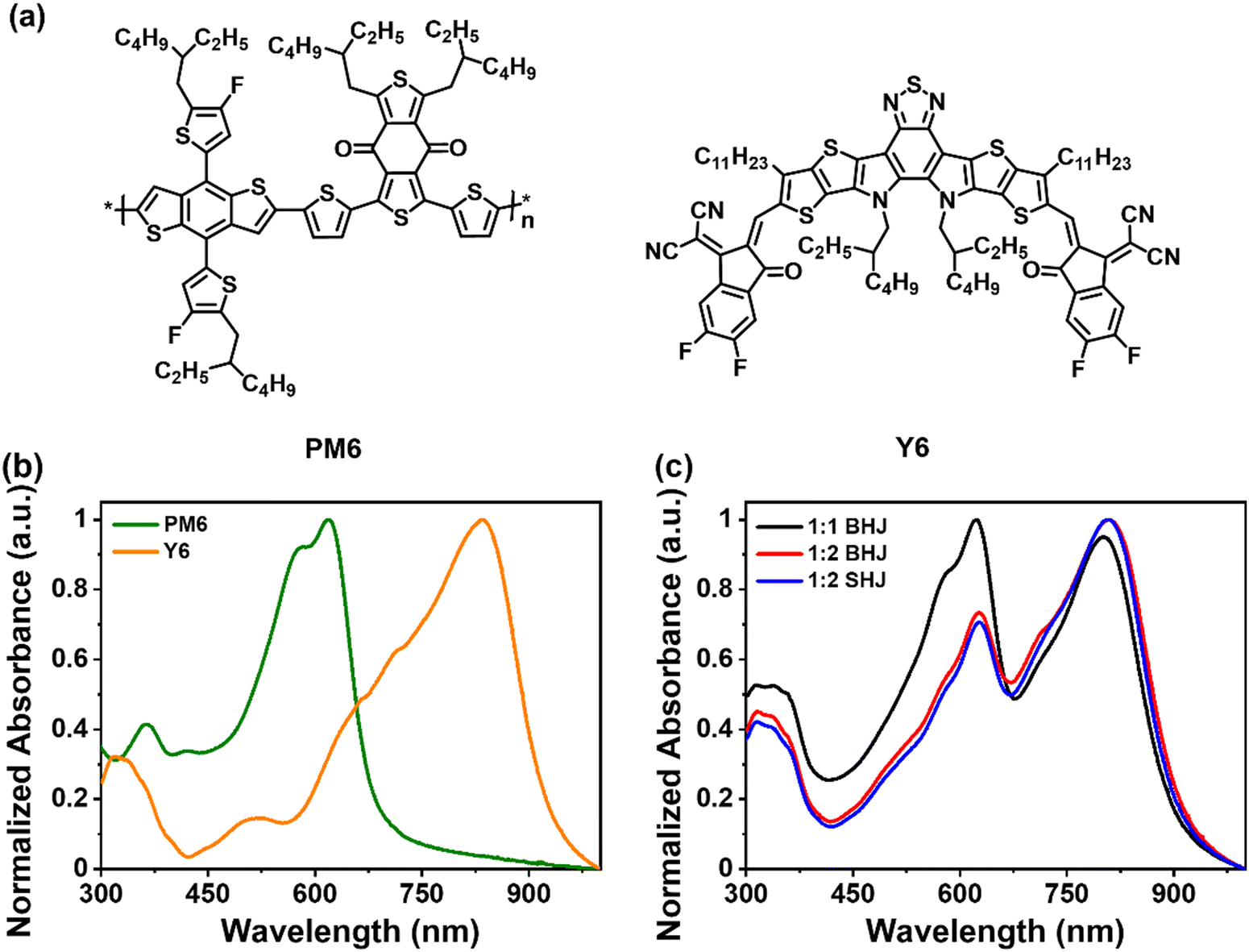 | ||
| Fig. 1 (a) Chemical structures of PM6 and Y6. (b) Normalized absorption spectra of PM6 and Y6 films. (c) Normalized absorption spectra of 1:1 BHJ, 1:2 BHJ and 1:2 SHJ films. | ||
Results and discussion
Photovoltaic properties
The PM6 film has a strong absorption at ca. 450–650 nm, while the Y6 film shows a broad absorption ranging from 600 nm to 900 nm, which is complementary with that of PM6 (Fig. 1b). Compared with the 1:1 BHJ blend film, the maximum absorption peak of the 1:2 BHJ blend film red-shifts from 624 nm to 809 nm (Fig. 1c). Decreasing donor content and increasing acceptor content are beneficial for reducing light absorption in the visible region and harvesting more photons in the near-infrared region. The 1:2 SHJ blend film exhibits a similar light absorption compared with the 1:2 BHJ blend film, with only slight reduction at 300–600 nm.
For the BHJ device, the donor:acceptor mixture was dissolved in advance and spin-coated in one step. For the SHJ device, the donor was deposited first, followed by spin coating of the acceptor solution, as shown in Fig. S1a (ESI†). To explore the photovoltaic performance of different PM6:Y6 blends, we firstly fabricated opaque devices with the structure of indium tin oxide (ITO) glass/PEDOT:PSS/active layer/PNDIT-F3N/Ag (Fig. S1b, ESI†). The thickness of the active layer was ca. 100 nm and the D:A weight ratios varied from 1:1 to 1:2. The 1:1 BHJ device exhibited a PCE of 14.9% with an open-circuit voltage (VOC) of 0.868 V, a short-circuit current density (JSC) of 25.6 mA cm−2, and a fill factor (FF) of 67.2%. The 1:2 BHJ device exhibited a relatively lower VOC of 0.844 V, a higher JSC of 26.2 mA cm−2, a similar FF of 67.9% and a comparable PCE of 15.0%. Compared with the 1:2 BHJ device, the 1:2 SHJ device delivered a high PCE of 16.1% with a similar VOC of 0.842 V, a JSC of 26.9 mA cm−2 and a significantly improved FF of 71.1% (Table 1). The current density–voltage (J–V) curves of the above devices under AM 1.5G illumination (100 mW cm−2) and corresponding external quantum efficiency (EQE) spectra are shown in Fig. 2a and b. The integrated JSC values of the above three devices are 24.7, 25.0 and 25.6 mA cm−2 (Table 1), which are consistent with the J–V results (mismatch less than 5%).
:1 BHJ, 1:2 BHJ and 1:2 SHJ devicesa
| Type | Device structure | V OC (V) | J SC (mA cm−2) | FF (%) | PCE (%) | Calc. JSC (mA cm−2) | AVT (%) |
|---|---|---|---|---|---|---|---|
| a Average values (in parentheses) are obtained from 15 devices. | |||||||
| Opaque | 1:1 BHJ |
0.868 (0.858 ± 0.007) | 25.6 (25.4 ± 0.4) | 67.2 (66.9 ± 1.2) | 14.9 (14.5 ± 0.4) | 24.7 | — |
| 1:2 BHJ |
0.844 (0.842 ± 0.002) | 26.2 (25.9 ± 0.6) | 67.9 (66.7 ± 1.6) | 15.0 (14.5 ± 0.3) | 25.0 | — | |
| 1:2 SHJ |
0.842 (0.840 ± 0.002) | 26.9 (26.4 ± 0.4) | 71.1 (69.8 ± 0.9) | 16.1 (15.5 ± 0.4) | 25.6 | — | |
| ST | 1:1 BHJ |
0.851 (0.852 ± 0.003) | 20.6 (20.1 ± 0.5) | 66.2 (65.4 ± 0.9) | 11.6 (11.2 ± 0.3) | 20.1 | 21.5 |
| 1:2 BHJ |
0.831 (0.831 ± 0.003) | 21.1 (20.9 ± 0.2) | 67.5 (67.0 ± 0.5) | 11.8 (11.6 ± 0.1) | 20.6 | 22.9 | |
| 1:2 SHJ |
0.831 (0.831 ± 0.006) | 21.4 (20.8 ± 0.6) | 70.6 (69.0 ± 1.1) | 12.5 (11.9 ± 0.4) | 20.5 | 25.4 | |
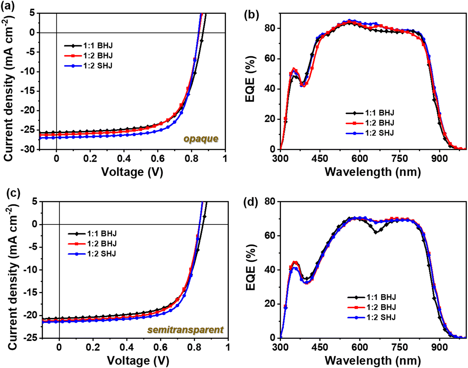 | ||
| Fig. 2 (a) J–V curves and (b) EQE spectra of 1:1 BHJ, 1:2 BHJ and 1:2 SHJ opaque devices. (c) J–V curves and (d) EQE spectra of 1:1 BHJ, 1:2 BHJ and 1:2 SHJ semitransparent devices. | ||
Then, we fabricated semitransparent devices with the structure of ITO glass/PEDOT:PSS/active layer/PNDIT-F3N/Au/Ag (Fig. S1c, ESI†). During ultrathin Ag electrode evaporation, Ag atoms tend to form discontinuous silver islands, which decreases the conductivity and transmittance of the Ag electrode. The ultrathin Au layer (ca. 1 nm) was vacuum-deposited onto the cathode interfacial layer, which can improve the uniformity and continuity of the ultrathin Ag electrode. Through adjusting the thickness of the Ag electrode, a series of ST-OSCs based on 1:1 BHJ, 1:2 BHJ and 1:2 SHJ have been fabricated (Table S1, ESI†). The ST-OSCs based on the 1:1 BHJ exhibit PCEs varying from 11.6% to 12.9%, with AVT values changing from 21.5% to 11.7%. The ST-OSCs based on the 1:2 BHJ exhibit PCEs varying from 11.8% to 12.6%, with AVT values changing from 22.9% to 12.2%. The ST-OSCs based on the 1:2 SHJ exhibit PCEs varying from 12.5% to 14.0%, with AVT values changing from 25.4% to 12.6%. The optimized ST-OSCs (Au layer: 1 nm; Ag layer: 10 nm) based on the 1:1 BHJ and 1:2 BHJ exhibited similar FFs of 66.2% and 67.5%, and comparable PCEs of 11.6% and 11.8%, respectively. Compared with the BHJ devices, the 1:2 SHJ device delivered a higher PCE of 12.5% with a significantly improved FF of 70.6% (Table 1 and Fig. 2c, d).
Optical characterization
Firstly, we investigated the optical properties of the 1:1 BHJ, 1:2 BHJ and 1:2 SHJ blend films, in which light-absorbing selectivity is one of the most important values. The light-absorbing selectivity is related to the light absorption and transmission ability in the visible region. The visible region is defined from 370 to 740 nm. By integrating the solar spectrum, the invisible photon energy power is calculated to be 48.02 mW cm−2 and the visible photon energy power is calculated to be 51.98 mW cm−2. The light-absorbing selectivity is defined as the product of absorbed energy ratio in the invisible region and transmitted energy ratio in the visible region as follows: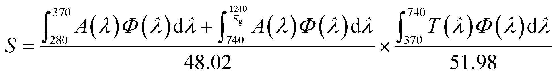 | (1) |
:1 BHJ, 1:2 BHJ and 1:2 SHJ films are shown in Fig. 1c and 3a, respectively. The light-absorbing selectivity of the 1:2 SHJ film is 0.1414, higher than that of the 1:1 BHJ film (0.1302) and the 1:2 BHJ film (0.1386), which indicates that the 1:2 SHJ film is more suitable for fabricating ST-OSCs.
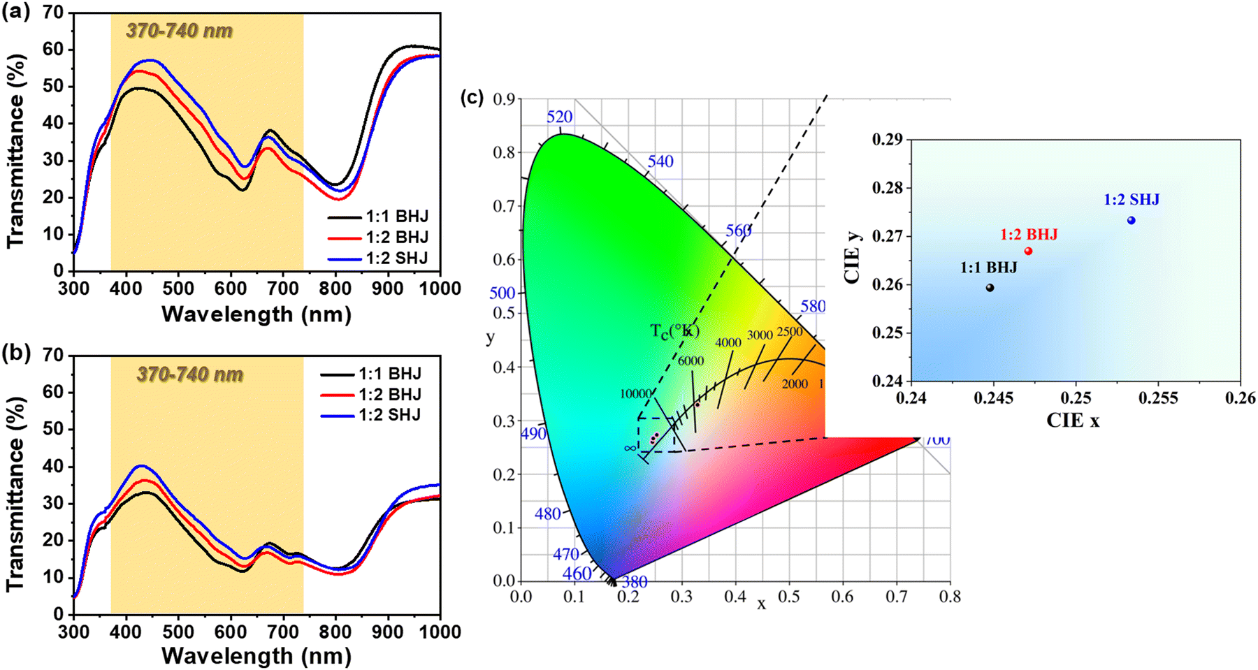 | ||
| Fig. 3 Transmittance spectra of (a) blend films and (b) the corresponding ST-OSCs based on 1:1 BHJ, 1:2 BHJ and 1:2 SHJ. (c) Colour coordinates of the ST-OSCs on a CIE chromaticity diagram. | ||
Then, we investigated the optical properties of the ST-OSCs. Fig. 3b displays the transmittance spectra of devices based on 1:1 BHJ, 1:2 BHJ and 1:2 SHJ structures. In order to describe the visibility of ST-OSCs, we calculated the average photopic transmission (APT) by the integration of the transmission spectrum and AM 1.5G photo flux weighted against the photo response of the human eye as follows
 | (2) |
:1 BHJ, 1:2 BHJ and 1:2 SHJ ST-OSCs were 17.6%, 20.2% and 22.9%, respectively. Apart from PCE, AVT and APT, light utilization efficiency (LUE) is another figure of merit to evaluate ST-OSCs (LUE = PCE × APT). The LUEs were calculated to be 2.04%, 2.38% and 2.86% for the 1:1 BHJ, 1:2 BHJ and 1:2 SHJ ST-OSCs, respectively. Among the three different kinds of ST-OSCs, the 1:2 SHJ device exhibited the best optical performance.
The Commission Internationale de L’Eclairage (CIE) 1931 chromaticity diagram describes the transparency color perceptions of the ST-OSCs (Fig. 3c). The colour coordinates of the 1:1 BHJ, 1:2 BHJ and 1:2 SHJ devices were (0.2448, 0.2594), (0.2471, 0.2669) and (0.2534, 0.2733). The corresponding correlated color temperatures (CCT) were 19439, 17133 and 14905 K (Table S2, ESI†), respectively. These values indicate that transmitted light of the 1:2 SHJ devices has a more neutral color sensation. Thus, the devices with SHJ structure show excellent visible light transparency.
Device physics and film morphology
In order to understand the reason for the FF enhancement in SHJ-based ST-OSCs, we investigated the device physics and active layer morphology. The exciton dissociation behavior in the devices was studied through the photocurrent density (Jph) vs. effective voltage (Veff) relationship (Fig. S2a, ESI†). The charge-transfer state dissociation probability is proportional to the ratio of JSC and saturated Jph (Jsat). The JSC/Jsat values for the optimized 1:1 BHJ, 1:2 BHJ and 1:2 SHJ devices are 96.7%, 97.2% and 97.2%, respectively, suggesting effective exciton dissociation existing in the above three devices. We further investigated the charge recombination of the 1:1 BHJ, 1:2 BHJ and 1:2 SHJ devices through JSCvs. light intensity (Plight) relationships. According to JSC ∝ Plightα,40 the α values are all 0.94 for the 1:1 BHJ, 1:2 BHJ and 1:2 SHJ devices, indicating weak bimolecular recombination in the above three devices (Fig. S2b, ESI†).
We employed the space charge limited current (SCLC) method to measure the charge mobilities of the 1:1 BHJ, 1:2 BHJ and 1:2 SHJ blend films (Fig. S2c, d and Table S3, ESI†).41 The μh values of the 1:1 BHJ, 1:2 BHJ and 1:2 SHJ blend films are 6.4 × 10⁻⁴ cm2 V−1 s−1, 5.6 × 10⁻⁴ cm2 V−1 s−1, and 6.3 × 10⁻⁴ cm2 V−1 s−1, respectively. The electron mobilities (μe) of the above three blends are 5.4 × 10⁻⁵ cm2 V−1 s−1, 4.4 × 10⁻⁴ cm2 V−1 s−1, and 7.9 × 10⁻⁴ cm2 V−1 s−1, respectively. Compared with BHJ blend films, the optimized 1:2 SHJ film exhibits higher and more balanced charge mobilities, which can reduce charge recombination and improve the FF.
Atomic force microscopy (AFM) was used to investigate the surface morphology of the 1:1 BHJ, 1:2 BHJ and 1:2 SHJ blend films (Fig. S3, ESI†). The root-mean-square roughness (Rq) values of the 1:1 BHJ, 1:2 BHJ and 1:2 SHJ blend films are 0.99 nm, 1.04 nm, and 1.10 nm, respectively, indicating smooth surface morphology of the above three blend films. Transmission electron microscopy (TEM) was adopted to investigate the bulky morphology of the 1:1 BHJ, 1:2 BHJ and 1:2 SHJ blend films (Fig. S4, ESI†). The TEM images of the above three blend films are similar.
Grazing incidence wide-angle X-ray scattering (GIWAXS) characterizations were performed to evaluate the molecular packing and orientation of the pure and blend films.42,43 The two-dimensional GIWAXS (2D GIWAXS) patterns and corresponding 1D line-cuts along the in-plane and out-of-plane directions of the 1:1 BHJ, 1:2 BHJ and 1:2 SHJ blend films are shown in Fig. 4. All BHJ and SHJ blend films exhibit face-on preferred orientation with strong (010) peaks in the out-of-plane direction. For the 1:1 BHJ blend film, the π–π stacking peak of Y6 locates at qz = 1.72 Å−1 (d-spacing of 3.65 Å), and the coherence length (CL) is 2.37 nm; the lamellar stacking peak of PM6 locates at qr = 0.29 Å−1 (d-spacing of 21.66 Å), and the corresponding CL value is 5.75 nm. For the 1:2 BHJ blend film, the Y6 π–π stacking peak locates at qz = 1.73 Å−1 (d-spacing of 3.63 Å), and CL is almost the same (2.38 nm); as for the PM6 lamellar stacking peak, it locates at qr = 0.29 Å−1 (d-spacing of 21.66 Å), and the corresponding CL value is 5.63 nm. Compared with the BHJ blend films, the 1:2 SHJ blend film exhibits stronger molecular ordering. The π–π stacking peak of Y6 locates at qz = 1.74 Å−1 (d-spacing of 3.61 Å), and the corresponding CL value increases to 2.68 nm. The lamellar stacking peak of PM6 also locates at qr = 0.29 Å−1 (d-spacing of 21.66 Å), and the corresponding CL value increases to 5.81 nm. In the 1:2 SHJ blend films, the PM6 and Y6 molecules exhibit a closer π–π stacking, leading to enhanced charge transport and FF.
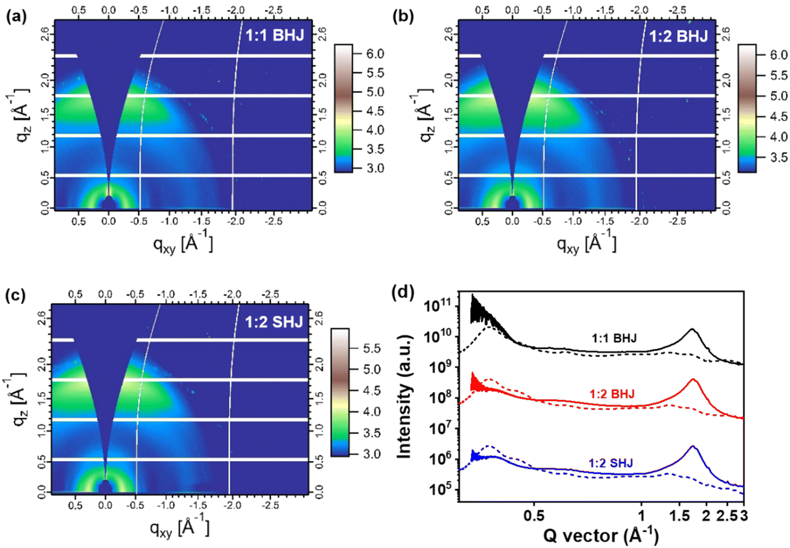 | ||
| Fig. 4 2D GIWAXS patterns of (a) 1:1 BHJ, (b) 1:2 BHJ and (c) 1:2 SHJ blend films. (d) Corresponding GIWAXS 1D line-cuts along the out-of-plane (solid lines) and in-plane (dashed lines) directions. | ||
Angle-dependent GIWAXS measurements were adopted to investigate the crystallinity change along the vertical direction.44–46 With larger incident angle, the X-ray beam penetrates the whole film depth, displaying an average structure of the entire film. Fig. S5 (ESI†) shows the GIWAXS 1D line-cuts of the 1:1 BHJ, 1:2 BHJ and 1:2 SHJ blend films with different incident angles (0.11°–0.15°). According to the in-plane (100) peaks (qr = 0.29 Å−1) and out-of-plane (010) peaks (qz = 1.72 Å−1), the lamellar stacking of the PM6 and the π–π stacking of the Y6 increase gradually with increasing incident angles. Compared to the 1:1 BHJ blend, greater enhancement of PM6 lamellar stacking can be observed for the 1:2 BHJ and 1:2 SHJ blend with increased incident angle, indicating bottom-enriched vertical distribution of PM6 with lower D/A ratio. The backbone stacking peaks of Y6 (located at ∼0.4 Å−1) are more apparent for the 1:2 BHJ and 1:2 SHJ blend, suggesting larger phase separation than the 1:1 BHJ blend. Compared with the 1:2 BHJ blend film, the changes of PM6 lamellar stacking and Y6 π–π stacking in the 1:2 SHJ blend film are more intensive with the increased angles, indicating that the 1:2 SHJ blend film has a more pronounced vertical phase separation. Film-depth-dependent light absorption spectroscopy was used to measure the vertical distribution of donor/acceptor.47–49 The donor/acceptor vertical segregation is different in BHJ and SHJ films as a result of different phase evolutions during film deposition. In the 1:1 BHJ blend film, the PM6 and Y6 materials exhibit no obvious phase separation in the vertical direction. The content of PM6 is slightly lower than that of Y6 in the lower half of the active layer (50–90 nm), and is slightly higher in the upper half (0–50 nm), which is not beneficial for charge transport and collection, leading to relatively lower JSC and FF. In the 1:2 BHJ blend film, the content of Y6 is >50% in the entire device. However, relatively high content of Y6 near the anode is not good for collecting holes, which still limits the FF of the devices. In contrast, in the 1:2 SHJ blend film, the vertical phase distribution is optimized. In the upper half of the active layer, especially at the active layer/PNDIT-F3N interface, the Y6 content is increased. In the lower half of the active layer, the PM6 content is increased, and can even reach 50% at the interface (Fig. 5a, c and e). The improved vertical phase distribution is beneficial for reducing charge recombination and improving charge transport, leading to higher JSC and FF. Then, the exciton generation contours were calculated via a modified transfer-matrix method (Fig. 5b, d and f),50 with the film-depth-dependent optical variations (Fig. S6, ESI†) as input. The maximum exciton generation rates (Gmax) of the 1:1 BHJ, 1:2 BHJ and 1:2 SHJ blend films were calculated to be 15.06 nm−3 s−1, 15.03 nm−3 s−1 and 15.14 nm−3 s−1, respectively (Fig. S7, ESI†), and the higher Gmax value accompanies more exciton generation, which is beneficial for JSC improvement.
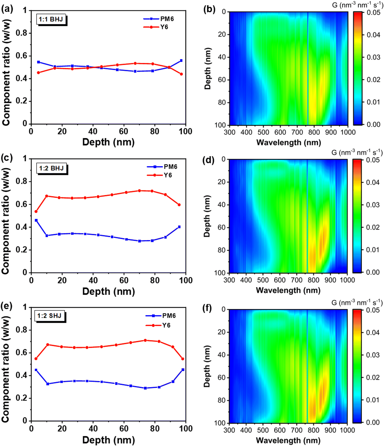 | ||
| Fig. 5 Donor/acceptor composition distribution as a function of film depth for (a) 1:1 BHJ; (c) 1:2 BHJ and (e) 1:2 SHJ blend films. Exciton generation contours (unit, 1016 mm−3 s−1 nm−1 at its position and wavelength) are calculated from the film-depth-dependent light absorption spectra (b, d and f) in combination with optical interference. The vertical noise-like lines in the contour are originally from the solar spectral profile of AM 1.5 G. The film depths 0 nm and 100 nm represent active layer/PNDIT-F3N and PEDOT:PSS/active layer interfaces, respectively. | ||
Conclusions
In summary, we have fabricated high-performance ST-OSCs based on wide-bandgap polymer donor PM6 and narrow-bandgap acceptor Y6, using diluted donor contents combined with a sequential solution process. Firstly, we decreased the ratio of PM6 in the PM6:Y6 BHJ blends to weaken the visible light absorption and to enhance device transparency in the visible region. Then, using low donor contents, we adopted a layer-by-layer solution process to fabricate SHJ ST-OSCs. Compared with BHJ devices, SHJ devices exhibited more proper donor/acceptor vertical separation, and higher and more balanced charge mobility, which is beneficial for increasing the FF of devices. The 1:2 SHJ ST-OSCs showed higher PCE, higher AVT and higher LUE than the BHJ counterpart. This work presented a useful method to achieve ST-OSCs with high efficiency and high transparency.
Conflicts of interest
The authors declare no conflict of interest.Acknowledgements
X. Z. thanks the NSFC (No. U21A20101). W. M. thanks the NSFC (21704082, 21875182), Key Scientific and Technological Innovation Team Project of Shaanxi Province (2020TD-002), and 111 Project 2.0 (BP2018008). GIWAXS data were acquired at beamlines 7.3.3 at the Advanced Light Source, which is supported by the Director, Office of Science, Office of Basic Energy Sciences, of the U.S. Department of Energy under Contract No. DE-AC02-05CH11231. The authors thank Dr Eric Schaible and Dr Chenhui Zhu at beamline 7.3.3 for assistance with data acquisition.Notes and references
- L. Lu, T. Zheng, Q. Wu, A. M. Schneider, D. Zhao and L. Yu, Chem. Rev., 2015, 115, 12666–12731 CrossRef CAS PubMed.
- C. Yan, S. Barlow, Z. Wang, H. Yan, A. K. Y. Jen, S. R. Marder and X. Zhan, Nat. Rev. Mater., 2018, 3, 18003 CrossRef CAS.
- J. Wang, P. Xue, Y. Jiang, Y. Huo and X. Zhan, Nat. Rev. Chem., 2022, 6, 614–634 CrossRef.
- Y. Lin, J. Wang, Z.-G. Zhang, H. Bai, Y. Li, D. Zhu and X. Zhan, Adv. Mater., 2015, 27, 1170–1174 CrossRef CAS PubMed.
- J. Yuan, Y. Zhang, L. Zhou, G. Zhang, H.-L. Yip, T.-K. Lau, X. Lu, C. Zhu, H. Peng, P. A. Johnson, M. Leclerc, Y. Cao, J. Ulanski, Y. Li and Y. Zou, Joule, 2019, 3, 1140–1151 CrossRef CAS.
- C. He, Y. Pan, Y. Ouyang, Q. Shen, Y. Gao, K. Yan, J. Fang, Y. Chen, C. Ma, J. Min, C. Zhang, L. Zuo and H. Chen, Energy Environ. Sci., 2022, 15, 2537–2544 RSC.
- R. Sun, Y. Wu, X. Yang, Y. Gao, Z. Chen, K. Li, J. Qiao, T. Wang, J. Guo, C. Liu, X. Hao, H. Zhu and J. Min, Adv. Mater., 2022, 34, 2110147 CrossRef CAS PubMed.
- Z. Zheng, J. Wang, P. Bi, J. Ren, Y. Wang, Y. Yang, X. Liu, S. Zhang and J. Hou, Joule, 2022, 6, 171–184 CrossRef CAS.
- Y. Li, X. Guo, Z. Peng, B. Qu, H. Yan, H. Ade, M. Zhang and S. R. Forrest, Proc. Natl. Acad. Sci. U. S. A., 2020, 117, 21147–21154 CrossRef CAS PubMed.
- C. Sun, R. Xia, H. Shi, H. Yao, X. Liu, J. Hou, F. Huang, H.-L. Yip and Y. Cao, Joule, 2018, 2, 1816–1826 CrossRef CAS.
- J. Wang, J. Zhang, Y. Xiao, T. Xiao, R. Zhu, C. Yan, Y. Fu, G. Lu, X. Lu, S. R. Marder and X. Zhan, J. Am. Chem. Soc., 2018, 140, 9140–9147 CrossRef CAS PubMed.
- S. Dai and X. Zhan, Adv. Energy Mater., 2018, 8, 1800002 CrossRef.
- W. Wang, C. Yan, T.-K. Lau, J. Wang, K. Liu, Y. Fan, X. Lu and X. Zhan, Adv. Mater., 2017, 29, 1701308 CrossRef PubMed.
- T. Li, S. Dai, Z. Ke, L. Yang, J. Wang, C. Yan, W. Ma and X. Zhan, Adv. Mater., 2018, 30, 1705969 CrossRef PubMed.
- P. Yin, Z. Yin, Y. Ma and Q. Zheng, Energy Environ. Sci., 2020, 13, 5177–5185 RSC.
- X. Huang, L. Zhang, Y. Cheng, J. Oh, C. Li, B. Huang, L. Zhao, J. Deng, Y. Zhang, Z. Liu, F. Wu, X. Hu, C. Yang, L. Chen and Y. Chen, Adv. Funct. Mater., 2021, 32, 2108634 CrossRef.
- P. Cheng, H.-C. Wang, Y. Zhu, R. Zheng, T. Li, C.-H. Chen, T. Huang, Y. Zhao, R. Wang, D. Meng, Y. Li, C. Zhu, K.-H. Wei, X. Zhan and Y. Yang, Adv. Mater., 2020, 32, 2003891 CrossRef CAS PubMed.
- J. Zhang, G. Xu, F. Tao, G. Zeng, M. Zhang, Y. Yang, Y. Li and Y. Li, Adv. Mater., 2019, 31, 1807159 CrossRef PubMed.
- Y. Wang, B. Jia, F. Qin, Y. Wu, W. Meng, S. Dai, Y. Zhou and X. Zhan, Polymer, 2016, 107, 108–112 CrossRef CAS.
- H. Park, J.-H. Lee, S. Lee, S. Y. Jeong, J. W. Choi, C.-L. Lee, J.-H. Kim and K. Lee, ACS Appl. Mater. Interfaces, 2020, 12, 2276–2284 CrossRef CAS PubMed.
- Z. Liu, P. You, S. Liu and F. Yan, ACS Nano, 2015, 9, 12026–12034 CrossRef CAS PubMed.
- L. Qin, J. Jiang, Q. Tao, C. Wang, I. Persson, M. Fahlman, P. O. Å. Persson, L. Hou, J. Rosen and F. Zhang, J. Mater. Chem. A, 2020, 8, 5467–5475 RSC.
- M. P. Ramuz, M. Vosgueritchian, P. Wei, C. Wang, Y. Gao, Y. Wu, Y. Chen and Z. Bao, ACS Nano, 2012, 6, 10384–10395 CrossRef CAS PubMed.
- J. Min, C. Bronnbauer, Z.-G. Zhang, C. Cui, Y. N. Luponosov, I. Ata, P. Schweizer, T. Przybilla, F. Guo, T. Ameri, K. Forberich, E. Spiecker, P. Bäuerle, S. A. Ponomarenko, Y. Li and C. J. Brabec, Adv. Funct. Mater., 2016, 26, 4543–4550 CrossRef CAS.
- G. Ji, Y. Wang, Q. Luo, K. Han, M. Xie, L. Zhang, N. Wu, J. Lin, S. Xiao, Y.-Q. Li, L.-Q. Luo and C.-Q. Ma, ACS Appl. Mater. Interfaces, 2018, 10, 943–954 CrossRef CAS PubMed.
- Q. Liu, L. G. Gerling, F. Bernal-Texca, J. Toudert, T. Li, X. Zhan and J. Martorell, Adv. Energy Mater., 2020, 10, 1904196 CrossRef CAS.
- Y. Li, C. He, L. Zuo, F. Zhao, L. Zhan, X. Li, R. Xia, H.-L. Yip, C.-Z. Li, X. Liu and H. Chen, Adv. Energy Mater., 2021, 11, 2003408 CrossRef CAS.
- R. Betancur, P. Romero-Gomez, A. Martinez-Otero, X. Elias, M. Maymó and J. Martorell, Nat. Photonics, 2013, 7, 995–1000 CrossRef CAS.
- Y. Li, C. Ji, Y. Qu, X. Huang, S. Hou, C.-Z. Li, L.-S. Liao, L. J. Guo and S. R. Forrest, Adv. Mater., 2019, 31, 1903173 CrossRef CAS PubMed.
- N. Schopp, G. Akhtanova, P. Panoy, A. Arbuz, S. Chae, A. Yi, H. J. Kim, V. Promarak, T.-Q. Nguyen and V. V. Brus, Adv. Mater., 2022, 34, 2203796 CrossRef CAS PubMed.
- Y. Tang, H. Zheng, X. Zhou, Z. Tang, W. Ma and H. Yan, Small Methods, 2022, 6, 2101570 CrossRef CAS PubMed.
- Y. Xie, Y. Cai, L. Zhu, R. Xia, L. Ye, X. Feng, H.-L. Yip, F. Liu, G. Lu, S. Tan and Y. Sun, Adv. Funct. Mater., 2020, 30, 2002181 CrossRef CAS.
- Z. Hu, Z. Wang and F. Zhang, J. Mater. Chem. A, 2019, 7, 7025–7032 RSC.
- K. Jiang, J. Zhang, Z. Peng, F. Lin, S. Wu, Z. Li, Y. Chen, H. Yan, H. Ade, Z. Zhu and A. K.-Y. Jen, Nat. Commun., 2021, 12, 468 CrossRef CAS PubMed.
- L. Zhan, S. Li, X. Xia, Y. Li, X. Lu, L. Zuo, M. Shi and H. Chen, Adv. Mater., 2021, 33, 2007231 CrossRef CAS PubMed.
- H. Ning, Q. Jiang, P. Han, M. Lin, G. Zhang, J. Chen, H. Chen, S. Zeng, J. Gao, J. Liu, F. He and Q. Wu, Energy Environ. Sci., 2021, 14, 5919–5928 RSC.
- Y. Wang and X. Zhan, Adv. Energy Mater., 2016, 6, 1600414 CrossRef.
- M. Zhang, X. Guo, W. Ma, H. Ade and J. Hou, Adv. Mater., 2015, 27, 4655–4660 CrossRef CAS PubMed.
- C. Yang, D. Liu, M. Bates, M. C. Barr and R. R. Lunt, Joule, 2019, 3, 1803–1809 CrossRef.
- P. Schilinsky, C. Waldauf and C. J. Brabec, Appl. Phys. Lett., 2002, 81, 3885–3887 CrossRef CAS.
- G. G. Malliaras, J. R. Salem, P. J. Brock and C. Scott, Phys. Rev. B: Condens. Matter Mater. Phys., 1998, 58, 13411–13414 CrossRef.
- F. Liu, Y. Gu, X. Shen, S. Ferdous, H.-W. Wang and T. P. Russell, Prog. Polym. Sci., 2013, 38, 1990–2052 CrossRef CAS.
- L. Zhang, X. Xu, B. Lin, H. Zhao, T. Li, J. Xin, Z. Bi, G. Qiu, S. Guo, K. Zhou, X. Zhan and W. Ma, Adv. Mater., 2018, 30, 1805041 CrossRef PubMed.
- G. Renaud, R. Lazzari and F. Leroy, Surf. Sci. Rep., 2009, 64, 255–380 CrossRef CAS.
- J. Wang, M. J. Bedzyk and M. Caffrey, Science, 1992, 258, 775–778 CrossRef CAS PubMed.
- Y. Wang, X. Wang, B. Lin, Z. Bi, X. Zhou, H. B. Naveed, K. Zhou, H. Yan, Z. Tang and W. Ma, Adv. Energy Mater., 2020, 10, 2000826 CrossRef CAS.
- L. Bu, S. Gao, W. Wang, L. Zhou, S. Feng, X. Chen, D. Yu, S. Li and G. Lu, Adv. Electron. Mater., 2016, 2, 1600359 CrossRef.
- T. Xiao, J. Wang, S. Yang, Y. Zhu, D. Li, Z. Wang, S. Feng, L. Bu, X. Zhan and G. Lu, J. Mater. Chem. A, 2020, 8, 401–411 RSC.
- P. Xue, S. Dai, T.-K. Lau, J. Yu, J. Zhou, Y. Xiao, K. Meng, Z. Xie, G. Lu, X. Lu, R. P. S. Han and X. Zhan, Sol. RRL, 2020, 4, 2000115 CrossRef CAS.
- Y. Huo, X.-T. Gong, T.-K. Lau, T. Xiao, C. Yan, X. Lu, G. Lu, X. Zhan and H.-L. Zhang, Chem. Mater., 2018, 30, 8661–8668 CrossRef CAS.
Footnote |
| † Electronic supplementary information (ESI) available. See DOI: https://doi.org/10.1039/d2tc04507a |
| This journal is © The Royal Society of Chemistry 2023 |