
 Open Access Article
 This Open Access Article is licensed under a Creative Commons Attribution-Non Commercial 3.0 Unported Licence
Air-stable high-PLQY cesium lead halide perovskites for laser-patterned displays†
Ping
Liu‡
ab,
Boyang
Yu‡
 c,
Wanqing
Cai‡
*d,
Xiongxian
Yao
ab,
Kai
Chang
c,
Xinyan
Zhao
c,
Zhichun
Si
b,
Weiwei
Deng
*c,
Yuanyuan
Zhou
*ef,
Guangmin
Zhou
*ab and
Guodan
Wei
*ab
c,
Wanqing
Cai‡
*d,
Xiongxian
Yao
ab,
Kai
Chang
c,
Xinyan
Zhao
c,
Zhichun
Si
b,
Weiwei
Deng
*c,
Yuanyuan
Zhou
*ef,
Guangmin
Zhou
*ab and
Guodan
Wei
*ab
aTsinghua-Berkeley Shenzhen Institute (TBSI), Tsinghua University, Shenzhen 518055, China. E-mail: weiguodan@sz.tsinghua.edu.cn; guangminzhou@sz.tsinghua.edu.cn; liuping19@mails.tsinghua.edu.cn; yaoxx21@mails.tsinghua.edu.cn
bInstitute of Materials Science, Tsinghua Shenzhen International Graduate School, Tsinghua University, Shenzhen 518055, China. E-mail: si.zhichun@sz.tsinghua.edu.cn
cDepartment of Mechanics and Aerospace Engineering, Southern University of Science and Technology (SUSTech), Shenzhen 518055, China. E-mail: dengww@sustech.edu.cn; 11930344@mail.sustech.edu.cn; changkai.work@foxmail.com; zhaoxy@sustech.edu.cn
dFaculty of Materials Science, MSU-BIT University, Shenzhen 518172, China. E-mail: wqcai@smbu.edu.cn
eDepartment of Applied Physics, The Hong Kong Polytechnic University, Hong Kong SAR, 999077, China. E-mail: yyzhou@hkbu.edu.hk
fSmart Society Laboratory, Hong Kong Baptist University, Kowloon, Hong Kong SAR, 999077, China
First published on 9th January 2023
Abstract
Metal halide perovskites (MHPs) have emerged as attractive building blocks for advanced photoluminescence display applications. But the practical deployment of MHP displays is hindered by the relatively low air stability, which can cause difficulty in high-precision film patterning under ambient conditions while achieving high photoluminescence quantum yields (PLQYs). Here we incorporate a polymer additive of poly(2-ethyl-2-oxazoline) (PEtOx) in the solution processing of quasi-2D phenylbutylamine bromide/cesium lead halide (PBABr/CsPbBr0.6I2.4) perovskite films, which not only results in a high PLQY of 91%, but more importantly improves the ambient stability via Lewis base–acid interaction of oxygen functional groups of the polymer and Pb of the perovskite. Using time-resolved optical spectroscopy and femtosecond transient absorption spectroscopy, we find that in the PEtOx-stabilized quasi-2D perovskite film, the trap-assisted nonradiative recombination rate is reduced while the radiative recombination is significantly promoted, underpinning the PLQY improvements. Via mask-less laser direct-write patterning onto this air-stable high-PLQY perovskite film, we have achieved complex-patterned displays on both rigid and flexible substrates, with anti-counterfeiting encryption code as a proof-of-concept demonstration. This work opens new opportunities for engineering perovskites to multifunctional display applications.
Introduction
Advanced photoluminescence displays are important in the area of anti-counterfeiting and information encryption, and searching for stable and efficient phosphor materials is the key to their commercial development. In the past years, carbon quantum dot materials1 and lanthanide luminescent inks2 have been mostly explored, but there are intrinsic drawbacks associated with these materials. For instance, carbon dots suffer from low fluorescence efficiency and poor color purity, making them easy to be duplicated. The costs of lanthanide materials are relatively high, rendering it difficult to apply them in large-scale anti-counterfeiting scenarios such as paper money. Recently, metal halide perovskites have emerged as an attractive material system for photoluminescence applications. In particular, their photoluminescent properties have been attested by their superior applications in a range of optoelectronic devices such as solar cells, light-emitting diodes (LEDs), photodetectors, and lasers.3For advanced display applications, perovskites exhibit various desirable properties, including tunable photo-emission, extended visible range activities, and high PLQYs. There have been a handful of efforts combining perovskite materials with conventional patterning technologies for anti-counterfeiting and information encryption applications.4 However, the poor air-stability remains one of the main obstacles for their practical application. Also, with regard to perovskite patterning, the conventional methods used are mostly lithography and inkjet printing.5 The former involves complex masking procedures and solvents for lithographic patterning.6 The latter relies on specially formulated perovskite inks with controlled viscosities and surface tensions, and the precision of patterning resulting from this solution process is limited.7 In this context, it remains challenging to obtain high-precision patterned perovskite films in ambient air without the use of masking,4b,8 which calls for the needs of both developing air-stable high-PLQY perovskite films and unconventional patterning methods.
In this work, by performing mask-less laser direct-write patterning onto this high-PLQY air-stable perovskite film, we achieved rigid and flexible complex patterned displays, with anti-counterfeiting encryption code as proof-of-concept demonstration. We demonstrated efficient and air-stable pure-red quasi-2D perovskite thin films based on PETOx polymer engineering via one-step spin-coating. Under optimized experimental conditions, the quasi-2D perovskite films yielded a single emission peak at 634 nm with a remarkable PLQY value of over 90%, which is among the best reported performance for quasi-2D pure-red perovskite thin films to date (Table S1, ESI†). PEtOx was used as a cross-linked polymer to form PBABr/CsPbBr0.6I2.4 perovskite/PEtOx composite thin films. As reported in a previous work,9 the oxygen atoms in the PEtOx were strongly coordinated with Pb2+ in the form of a Lewis base–acid interaction, forming Lewis adducts with PbI2 through Pb–O bonds,10 thus enhancing the air stability and suppressing the humidity effect. It is well-known that photoluminescence (PL) efficiency is highly dependent on the competition between radiative (krad) and non-radiative (knonrad) recombination rates. Therefore, detailed investigation and direct experimental support are provided in our work to reveal the underlying mechanisms of high PLQYs in PEtOx treated perovskite thin films. The simple laser direct-write patterning procedure used here is a convenient and effective technique for large-area fabrication without any demand of a vacuum environment, high temperature, or complicated post-processing. No solvent or lift-off procedure is needed, thus avoiding the dissolution problem of perovskites in common polar solvents. The excellent optoelectronic properties of perovskite materials are preserved throughout the fabrication process. Our work demonstrates the great potential of this high PLQY perovskite for photoluminescence display applications and may pave the way for exploration of perovskite micro- and nanoscale light emitting devices.
Results and discussion
The process of preparing light emitting quasi-2D perovskite/PEtOx films via laser direct-write patterning is shown in Fig. S1 (ESI†). Typically, 3D CsPbBr0.6I2.4 perovskite solutions were prepared by mixing CsPbI3 and CsPbBr3 precursor solutions with a 4![[thin space (1/6-em)]](https://www.rsc.org/images/entities/char_2009.gif) :1 volume ratio. Organic salt phenylbenzyl ammonium bromide (PBABr) was added to the CsPbBr0.6I2.4 solutions with a certain molar ratio of 0.6:1 to synthesize quasi-2D PBABr/CsPbBr0.6I2.4. To achieve the goal of obtaining high-quality and stable perovskite films with high PLQYs, we introduced polymer PEtOx additives into the 3D CsPbBr0.6I2.4 precursor solution to assist the growth of perovskite crystals in PBABr/CsPbBr0.6I2.4/PEtOx composite thin films. The detailed results of PLQY optimization of the composite films by varying the molar ratio of PBABr, weight ratio of PEtOx and annealing temperature are shown in Fig. S2, ESI.† Considering the 91% PLQY and a dominant PL peak at 634 nm, we chose 0.6 molar ratio of PBABr and 20% weight ratio of PEtOx as the optimal ratio for the composite films. All perovskite thin films were prepared by spin coating the mixture solutions evenly at 4000 rpm for 45 s onto the glass substrate, followed by thermal annealing at 110 °C for 10 min to promote the crystallization. Subsequently, we use laser direct-write patterning to obtain the fine patterns of stable perovskite films, as described in the Experimental section.
:1 volume ratio. Organic salt phenylbenzyl ammonium bromide (PBABr) was added to the CsPbBr0.6I2.4 solutions with a certain molar ratio of 0.6:1 to synthesize quasi-2D PBABr/CsPbBr0.6I2.4. To achieve the goal of obtaining high-quality and stable perovskite films with high PLQYs, we introduced polymer PEtOx additives into the 3D CsPbBr0.6I2.4 precursor solution to assist the growth of perovskite crystals in PBABr/CsPbBr0.6I2.4/PEtOx composite thin films. The detailed results of PLQY optimization of the composite films by varying the molar ratio of PBABr, weight ratio of PEtOx and annealing temperature are shown in Fig. S2, ESI.† Considering the 91% PLQY and a dominant PL peak at 634 nm, we chose 0.6 molar ratio of PBABr and 20% weight ratio of PEtOx as the optimal ratio for the composite films. All perovskite thin films were prepared by spin coating the mixture solutions evenly at 4000 rpm for 45 s onto the glass substrate, followed by thermal annealing at 110 °C for 10 min to promote the crystallization. Subsequently, we use laser direct-write patterning to obtain the fine patterns of stable perovskite films, as described in the Experimental section.
The X-ray diffraction (XRD) spectra of all samples shown in Fig. 1a confirm the formation of CsPbI3 perovskites with stable crystalline black phase. By contrast, thin film PBABr/CsPbBr0.6I2.4 shows various strong diffraction peaks at 12°, 14.5° and 29°, verifying a better quasi-2D layered crystallinity with small n (n = the number of PbI4 perovskite layers). In addition, for thin film PBABr/CsPbBr0.6I2.4/PEtOx, the diffraction peaks at around 14.5° and 29.0° reveal (100) and (200) crystalline planes of black phase CsPbI3, respectively, while no obvious diffraction peaks corresponding to layered quasi-2D perovskites are observed.11 This indicates the formation of quasi-2D perovskite thin films with large n for PBABr/CsPbBr0.6I2.4/PEtOx. To investigate the effects of PEtOx polymer additives on the morphology of quasi-2D perovskite thin films, SEM and AFM measurements were performed, and the statistical data are shown in Table S2 (ESI†). As exhibited in Fig. 1b–d, the introduction of PEtOx additives onto quasi-2D perovskites can substantially improve the surface coverage of films, showing a decreased grain size and increased number density of grains. We can clearly observe that the PEtOx-treated sample has the smallest grain size. The reduced grain size implies an enhanced exciton confinement, thus an increased PLQY can be expected.12 Meanwhile, the root-mean-square roughness (Ra) of the perovskite thin films was extracted from the AFM results, shown in Fig. 1e–g. We can see that the Ra value of the PBABr/CsPbBr0.6I2.4/PEtOx sample is about 2.75 nm, which is much lower than that of the control sample (9.83 nm, shown in Fig. S3, ESI†), demonstrating the improved quality of the thin films. In a word, the improved surface coverage, reduced grain size, and decreased surface roughness together confirm the positive effect of PEtOx treatment on the morphology quality of quasi-2D perovskite films, suggesting their application potential for light-emitting displays and devices.
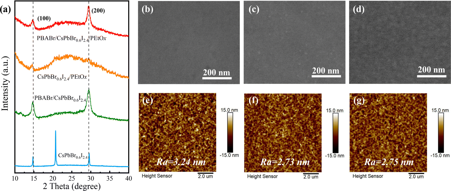 | ||
| Fig. 1 (a) Powder X-ray diffraction patterns of CsPbBr0.6I2.4 thin films with different additives on glass substrates. (b–d) SEM images, and (e–g) AFM images showing the surface morphologies of CsPbBr0.6I2.4 thin films with different additives at the same annealing temperature. From left to right: PBABr/CsPbBr0.6I2.4, CsPbBr0.6I2.4/PEtOx and PBABr/CsPbBr0.6I2.4/PEtOx. | ||
Furthermore, we explored the optical properties of the light emitting PBABr/CsPbBr0.6I2.4/PEtOx composite thin films. As depicted in Fig. 2a, thin film PBABr/CsPbBr0.6I2.4/PEtOx possess pure-red emission at 634 nm, which is analogous to thin film PBABr/CsPbBr0.6I2.4, demonstrating that the addition of PEtOx will not change the composition and crystallinity of quasi-2D perovskites. The PL spectra reveal the fact that energy transfers from larger band gap to smaller band gap quasi-2D perovskites.13 To quantitatively evaluate the emission intensity, the PLQY is measured. As shown in Fig. 2b, for thin film PBABr/CsPbBr0.6I2.4/PEtOx, the PLQY increased remarkably to 91%, over 5 times higher than that of thin film PBABr/CsPbBr0.6I2.4. Meanwhile, the environmental stabilities of CsPbBr0.6I2.4 thin films with different additives were investigated. The moisture stability test was performed under high humidity conditions (temperature = 298 K, relative humidity RH = 50%) without encapsulation, and the PL spectra were continuously monitored in the process of aging tests. As exhibited in Fig. 2c, the PLQY of thin films PBABr/CsPbBr0.6I2.4 and CsPbBr0.6I2.4/PEtOx gradually decreased with time, exhibiting a nearly total (∼100%) emission degradation. In comparison, for sample PBABr/CsPbBr0.6I2.4/PEtOx, the PLQY can maintain over 40% of the initial emission level after the 24 hours aging test without encapsulation. It is also noteworthy that the peak wavelength and spectral profile of the PL spectra remained almost unchanged over the entire test shown in Fig. 2d. The corresponding PLQYs of the PBABr/CsPbBr0.6I2.4/PEtOx composite films with different concentrations of PEtOx were measured and are shown in Fig. S4a (ESI†). The PLQY increased with an increasing PEtOx concentration of up to 20%, showing a maximum PLQY of 91%; further increasing the PEtOx concentration resulted in a drop of PLQY. The decrease of PLQY may be due to the increase in the crystal size as revealed by SEM (Fig. S4c, ESI†), which leads to a phase separation between the polymer and perovskite phases at higher polymer blending ratios.9 We have also tested the stability of perovskite films with different concentrations of PEtOx shown in Fig. S4b (ESI†). Compared to composite perovskite films with 20% PEtOx, PLQY could only maintain 15% of the initial emission level after 24 h aging test for the sample containing 30% PEtOx. The results show that, as a protective agent, an appropriate PEtOx network could provide physical isolation to protect the quasi-2D perovskite films from high humidity, resulting in improved environment stability.
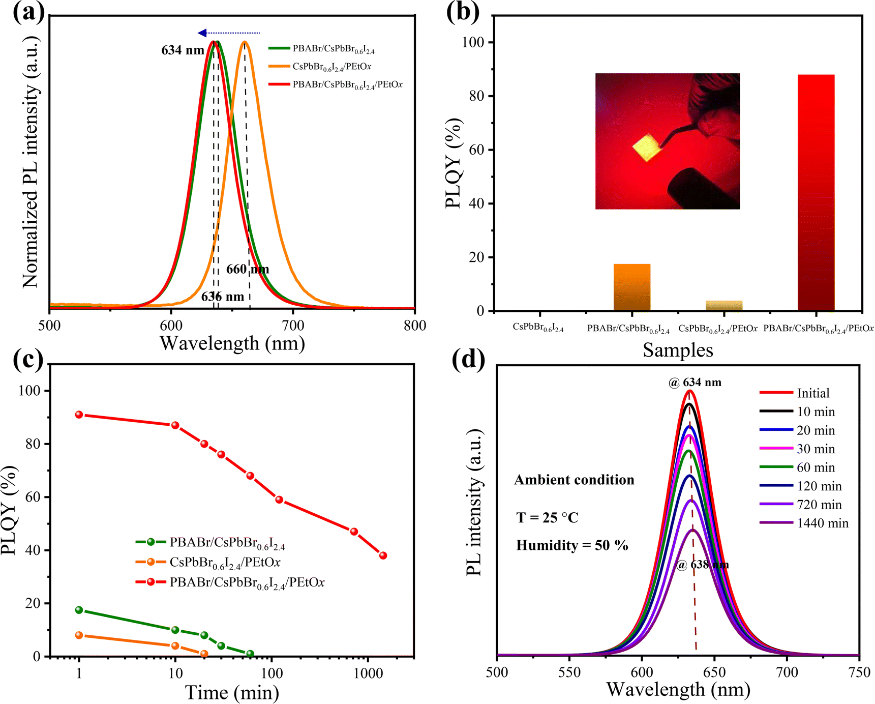 | ||
| Fig. 2 Optical properties of CsPbBr0.6I2.4 thin films with different additives, (a) PL spectra. (b) PLQYs, inset shows the photograph of the 91% PLQY perovskite film under 365 nm UV light irradiation. (c) Stability test of CsPbBr0.6I2.4 thin films with different additives under ambient conditions (temperature = 298 K, RH = 50%): time-dependent PLQYs, excitation wavelength: 365 nm. (d) Time-dependent PL spectra of thin film PBABr/CsPbI2.4Br0.6/PEtOx. | ||
The carrier recombination dynamics play a crucial role in emission behavior. In perovskites, the excited charge carrier dynamics upon photoexcitation undergo decoherence, thermalization, polaron formation, and cooling in the conduction band in the fast timescale of 1 ps, followed by different recombination pathways that relax the carriers to the valence band,14 as illustrated in Fig. S5 (ESI†). The radiative efficiency η, or the PLQY, could be expressed by the following equation:15
 | (1) |
To quantitatively analyze the recombination dynamics of PBABr/CsPbBr0.6I2.4 and PBABr/CsPbBr0.6I2.4/PEtOx thin films, we first investigated the k1 through TRPL measurements under extremely low excitation power (Fig. S6, ESI†), where the trap-assisted recombination dominates and high-order recombination contribution is inappreciable.17 As calculated, the thin film PBABr/CsPbBr0.6I2.4/PEtOx (k1:0.21 × 10⁷ s−1) possesses a lower trap-assisted non-radiative recombination rate than thin film PBABr/CsPbBr0.6I2.4 (k1:4.7 × 10⁷ s−1), attributable to the better interface passivation as PEtOx is introduced.18 To further verify the above conclusion, we directly characterize the defect densities using space-charge limited current measurement with a device structure of ITO/PEDOT/perovskite/MoO3/Ag (Fig. S7, ESI†). As expected, thin film PBABr/CsPbBr0.6I2.4/PEtOx shows a relatively lower defect density of 1.3 × 1016 cm−3 compared to thin film PBABr/CsPbBr0.6I2.4 (8.6 × 1016 cm−3).19
Fig. 3 shows the recombination dynamics of CsPbBr0.6I2.4 thin films with or without PEtOx additives under various excitation powers. In Fig. 3a, with 400 nm excitation, ground state bleaching (GSB) signals were observed at 448 nm (n = 2) and 540 nm (n = 3), demonstrating the generation of excited states in the n = 2 and n = 3 domains for the 0.6PBABr-CsPbBr0.6I2.4-0% PEtOx thin film. In contrast, for the thin film with 20% PEtOx, the 540 nm (n = 3) signals became weak, and the 448 nm (n = 2) signal disappeared, while only the signals at 600 nm (n ≥ 4) remained (Fig. 3b)) And the initial TA bleach signals plotted over pump power for perovskite thin films are shown in Fig. S8 (ESI†), which indicate that they are in the unsaturated absorption region.
 | ||
| Fig. 3 The recombination dynamics of CsPbBr0.6I2.4 thin films with different additives. The pseudo-color maps of thin films PBABr/CsPbBr0.6I2.4 (a) and PBABr/CsPbBr0.6I2.4/PEtOx (b) under an excitation power of 29 μW. The transient absorption spectra of thin film PBABr/CsPbBr0.6I2.4 (c), PBABr/CsPbBr0.6I2.4/PEtOx (d) under 1 ps delay time with various excitation densities. (e and f) The relationship between carrier recombination decay rates and carrier density. | ||
Subsequently, the charge-carrier recombination kinetics can be quantitatively described by the following equation:20
 | (2) |
The k2 and k3 can be extracted by fitting TA spectra under various excitation fluences with eqn (2) (Fig. 3c–f).21 The fitting results are summarized in Table 1 and the calculation details can be referred to from the previous reports generated by Du et al.22 The bi-molecular recombination constant k2 of PBABr/CsPbBr0.6I2.4/PEtOx is about 8 times higher than that of PBABr/CsPbBr0.6I2.4, indicating enhanced radiative recombination rate with stronger carrier confinement in the sample with PEtOx additives.
| Sample | k 1 (s−1) | k 2 (cm3 s−1) | k 3 (cm6 s−1) |
|---|---|---|---|
| The k1 is extracted from time-resolved PL under the low excitation fluence, and k2 and k3 are obtained from the global fitting of recombination rates–carrier density curves. | |||
| PBABr/CsPbBr0.6I2.4 | 4.7 × 10⁷ | 1.8 × 10⁻¹⁰ | 1.3 × 10⁻²⁷ |
| PBABr/CsPbBr0.6I2.4/PEtOx | 0.21 × 10⁷ | 9.4 × 10⁻¹⁰ | 6.1 × 10⁻²⁷ |
As expected, the measured PLQY of PBABr/CsPbBr0.6I2.4/PEtOx (91%) is indeed higher than that of PBABr/CsPbBr0.6I2.4 (18.5%) under a moderate excitation fluence. We note that the Auger recombination constant k3 of PBABr/CsPbBr0.6I2.4/PEtOx is also about 5 times higher than that of PBABr/CsPbBr0.6I2.4, which are attributed to the smaller CsPbBr0.6I2.4 nano-grains and stronger confinement.15b Therefore, the addition of the PEtOx polymer can not only reduce the trap-assisted recombination rate k1 but also significantly increase the bi-molecular recombination rate k2, which is promising to improve the PLQY of the perovskite thin film. On the basis of the above discussion, the enhanced PLQY can be attributed to the suppressed non-radiative loss as well as the remarkably increased radiative recombination rate by PEtOx additive engineering. Moreover, the results demonstrate the stability of perovskite thin film PBABr/CsPbBr0.6I2.4/PEtOx in air. This is evident that PEtOx treated perovskite films with pure-red emission are compatible for practical optoelectronic domains even in an air environment.
The principle of the laser direct-write patterning method used in this work is based on steering the pulsed and focused laser beam by two orthogonal scanning mirrors driven by galvanometers. The material of the perovskite thin film is selectively removed by the laser. The pre-programmed removal pattern is realized by the two scanning mirrors combined with on/off control of the laser pulse. The detailed laser writing setup is schematically shown in Fig. S9 (ESI†). Considering the significance of wafer-scale fabrication of perovskite fluorescence patterns for various light-emitting application, we prepared large-area fluorescent perovskite thin film patterns with PLQY as high as 56% on a glass substrate by laser direct-write patterning. Due to the high-quality and uniform surface of the perovskite films, we can realize an ultrafast-laser direct patterning process without mask or any other complex lift-off procedure.23 By optimizing the pulse duration, repetition rate, and pulse energy, a series of patterns can be obtained. As shown in Fig. 4a, the fluorescence image of the macroscopic letters “TBSI” with bright pure-red emission in millimeter scale was prepared. The enlarged SEM images confirmed that the perovskite thin film patterns exhibited excellent homogeneity, stability and reproducibility (Fig. 4b). The photoluminescence peak position is located at 645 nm (Fig. 4c) after the laser etching process, showing pure-red emission. It is noteworthy that the PL spectrum is red-shifted slightly. The representative XRD patterns of the perovskite films before and after laser etching are shown in Fig. S10 (ESI†). Strong (100) and (200) diffraction peaks were observed, indicating that both of the perovskite films have cubic structures. After laser etching, the two XRD peaks become narrower, suggesting the growth of CsPbBr0.6I2.4 crystals. In addition, a new peak located at 20.8° (marked by stars) appeared, which correspond to the δ phase of CsPbI3.24 Furthermore, after laser etching, the crystal size in the perovskite film became enlarged compared with the pristine one, shown in the SEM images (Fig. S11, ESI†). The conclusion can be drawn that the red shift of the PL spectrum was related to the crystal size change caused by laser etching heating.25
 | ||
| Fig. 4 Perovskite fluorescence patterns on various substrates via laser etching. (a) Fluorescence image of the laser-etched macroscopic letters “TBSI” in the perovskite film. (b) Enlarged SEM image of the letter “S”. The scale bar of (b) is 500 μm. (c) PL spectra of the perovskite fluorescence patterns after laser etching. (d and e) Two-dimensional code of “Tsinghua University”. The scale bars are 2 mm. (f and g) Digital photographs and fluorescence images of large-area flexible perovskite bended patterns on PC substrates using the laser direct-write patterning method. The scale bars are 2 mm. | ||
In addition, this direct laser patterning technique can be used to prepare any well-designed patterns. Benefiting from the substantially enhanced emission performance and material stability after PEtOx treatment, the resulting perovskite thin films may act as a smart and security pattern in anti-counterfeiting applications. Thus, a two-dimensional code was prepared (Fig. 4d and e). Through this direct laser patterning method, anti-counterfeiting information can be hidden, and it is difficult for a counterfeiter to imitate in a printed invisible pattern. Under UV light irradiation, the appearance of a bright red two-dimensional code containing the information of “Tsinghua University” can be clearly seen. The processes of encrypting and decrypting were implemented using UV light on/off as a switch. It implied a promising application in multidimensional information encoding and anticounterfeiting.
Compared with microfabrication techniques,23,26 this laser direct patterning method is efficient and inexpensive. All of these patterns were transparent and stable in the ambient environment. Meanwhile, our approach can be extended to other types of metal halide perovskites such as perovskite quantum dots (QDs) and vacuum-deposited perovskites, as well as flexible substrates such as polydimethylsiloxane (PDMS), polycarbonate (PC), polyethylene terephthalate (PET) films, etc. Herein, without any other complex lift-off procedure or being transferred to flexible substrates, we obtained large-area fluorescence flexible patterns via the laser direct-write patterning method directly on the PC substrate. As shown in Fig. 4f and g, the fluorescence images of the complicated patterns of two-dimensional code of Tsinghua University were prepared, showing bright red fluorescence under UV light. These patterns could be bended to different angles, showing good flexibility. The above results indicated that these high PLQY perovskite thin films via the laser direct-write patterning method show diverse potential for wearable light-emitting devices and flexible panel display applications.27
Conclusions
In summary, significant enhancement of the PLQY and stability in quasi-2D perovskite thin films was achieved by PEtOx engineering via a one-step method, where the PLQY was boosted to 91% from the initial value of 18.5%. Time-resolved optical measurements and femtosecond-transient absorption revealed that PEtOx treated quasi-2D perovskites induced a remarkably suppressed non-radiative loss by 5 times and a promoted radiative recombination rate by 8 times, which together contribute to the PL enhancement. Moreover, we have succeeded in developing a high resolution, large-area laser etching patterning method to pattern perovskite thin films. Taking advantage of the uniformity of the perovskite thin film and the generic etching approach, various pure-red single-color patterns have been successfully fabricated. Compared with microfabrication techniques, this etching method is efficient and economic. It opens opportunities to fabricate all laser etching perovskite optoelectronic devices and may extend for exploring other types of materials for a wide range of applications. Further study should continue to improve device performance by balancing the high PL and efficient carrier injection via additive optimization and further improving device stability.Experimental section
Materials
Cesium iodide (CsI, 99.999%), cesium bromide (CsBr, 99.999%) and lead bromide (PbBr2, 99.999%) were purchased from Sigma Aldrich; lead iodide (PbI2, 99.999%) was bought from Xi’an Polymer Light Technology Crop; poly(2-ethyl-2-oxazoline) (PEtOx) polymer with average molecular weight of 50000 was purchased from Sigma Aldrich; phenylbutylamine bromide (PBABr) was purchased from Xi’an Polymer Light Technology Crop; anhydrous dimethyl sulfoxide (DMSO, ≥99.9%) was purchased from Sigma-Aldrich; poly[bis(4-phenyl)(4-butylphenyl)amine] (poly-TPD) purchased from American Dye Source (Canada) was utilized; ZnMgO/ethanol (50 mg mL−1) solution was purchased from Guangdong Poly Optoelectronics Crop. All materials and reagents were used as received without further purification.
Preparation of quasi-2D perovskite thin films
CsI and PbI2 were dissolved in DMSO with a molar ratio of 1:1 to form a 0.25 M CsPbI3 precursor solution. CsBr and PbBr2 were dissolved in DMSO with a molar ratio of 1:1 to form a 0.25 M CsPbBr3 precursor solution. CsPbBr0.6I2.4 solutions were fabricated by mixing CsPbI3 and CsPbBr3 precursor solutions with a 4:1 volume ratio. Organic salt PBABr was dissolved in DMSO at a concentration of 0.5 M. PEtOx was dissolved in DMSO with a concentration of 100 mg mL−1. Appropriate amounts of PEtOx with a weight ratio of 20% (wPEtOx:wPb = 20%) was added to the CsPbBr0.6I2.4 solutions to gain CsPbBr0.6I2.4/PEtOx. The weight ratio of PEtOx to CsPbBr0.6I2.4 solutions remained as 20% in all the fabricated perovskite films while the molar ratio of PBABr was varied. Right before spin coating, the precursor solutions were stirred overnight and filtered by a 0.22 μm polytetrafluoroethylene (PTFE) syringe filter. The mixture precursor was spun-cast upon glass or flexible substrates at 4000 rpm for 45 s, followed by thermal annealing at a temperature of 110 °C for 10 min. A ∼50 nm thick quasi-2D perovskite/PEtOx composite thin film was obtained.
Characterization of perovskite thin films
XRD data were obtained using a D8 advance X-ray diffraction instrument with Cu Kα source in the range of 10°–50°. The photoluminescence (PL) spectra and photoluminescence quantum yields (PLQYs) of perovskite thin films were obtained with an XPQY spectrometer (Xipu Optoelectronics Crop) under the irradiation of the 365 nm laser. Emission decay kinetics with Time Resolution Photoluminescence (TRPL) spectra were obtained using an Edinburgh FS5 fluorescence spectrometer at room temperature using time-correlated single photon counting (TCSPC; 1024 channels; 500 ns window) with data collection for 3000 counts. For transient absorption (TA) measurements, femtosecond laser pulses of an 800 nm fundamental beam (1 kHz repetition rate, 35 fs pulse width) were produced using a Ti:sapphire oscillator seeded regenerative amplifier (Spectra Physics, Spitfre Ace). Part of the 800 nm laser beam passed through a BBO crystal to generate a 400 nm beam by second harmonic generation, which served as a narrowband pump. The other part was focused onto a 1 mm sapphire plate to generate a white-light supercontinuum probe. Both the pump and probe pulses were directed into a commercial TA spectrometer (Helios, Ultrafast Systems). The surface morphologies of the perovskite thin films in the sample structure of the ITO/ZnMgO/perovskite were investigated with a Hitachi SU8010 cold field emission scanning electron microscope (SEM). The surface roughness and thickness of different perovskite thin films were measured using an atomic force microscope (AFM).Laser etching characterization
After the preparation of films via spin coating and thermal annealing, we use a direct laser to etch out the excess film and obtain certain patterns. We use a direct UV laser produced by 3K Laser Technology Co., Ltd, with a wavelength of 355 nm, a maximum power of 3 W, and a laser frequency of 30 kHz. The pattern required for etching is filled with a straight line with a spacing of 0.01 mm, and the laser sweeps through the surface of the film at a speed of 500 mm s−1. Flexible laser direct-write patterning patterns were obtained using a polycarbonate (PC) plastic substrate. The PL images of the patterned perovskite film were collected by confocal fluorescence microscopy. It is noted that all the laser direct-write patterning procedures are conducted in an air environment outside the glovebox without encapsulation.Author contributions
P. L., B. Y. Y. and W. Q. C. contributed equally to this work. P. L. wrote the manuscript, carried out the experiments of device fabrication, performance characterization and data analysis; B. Y. Y. and X. Y. Z. carried out the experiments of laser direct patterning; W. Q. C. helped to complete the idea and achieve the TA results; X. X. Y. assisted in the photoluminescence measurements; K. C. assisted in the exploration of laser etching experiments; G. D. W., W. W. D. and Y. Y. Z. led the project and supervised the research. All authors contributed to revising the manuscript.Conflicts of interest
The authors declare no competing financial interest.Acknowledgements
We acknowledge the funding support from the National Natural Science Foundation of China (Grant Numbers: 52027817, 11932009), the Science and Technology Planning Project of Shenzhen Municipality (Grant number: JCYJ20200109144615514), and the Shenzhen Science and Technology Innovation Committee (Grant number: RCBS20210706092343014).References
- S. Kalytchuk, Y. Wang, K. Polakova and R. Zboril, ACS Appl. Mater. Interfaces, 2018, 10, 29902–29908 CrossRef CAS PubMed.
- J. Andres, R. D. Hersch, J. E. Moser and A. S. Chauvin, Adv. Funct. Mater., 2014, 24, 5029–5036 CrossRef CAS.
- (a) S. Bai, P. Da, C. Li, Z. Wang, Z. Yuan, F. Fu, M. Kawecki, X. Liu, N. Sakai, J. T. Wang, S. Huettner, S. Buecheler, M. Fahlman, F. Gao and H. J. Snaith, Nature, 2019, 571, 245–250 CrossRef CAS PubMed; (b) C. C. Zhang, Z. K. Wang, S. Yuan, R. Wang, M. Li, M. F. Jimoh, L. S. Liao and Y. Yang, Adv. Mater., 2019, 31, e1902222 CrossRef PubMed; (c) S.-H. Jeong, H. Cho, M.-H. Park, Y.-H. Kim, C. Wolf, C.-L. Lee, J. H. Heo, A. Sadhanala, N. Myoung, S. Yoo, S. H. Im, R. H. Friend and T.-W. Lee, Science, 2015, 350, 1222–1225 CrossRef PubMed; (d) B. Zhao, S. Bai, V. Kim, R. Lamboll, R. Shivanna, F. Auras, J. M. Richter, L. Yang, L. Dai, M. Alsari, X.-J. She, L. Liang, J. Zhang, S. Lilliu, P. Gao, H. J. Snaith, J. Wang, N. C. Greenham, R. H. Friend and D. Di, Nat. Photonics, 2018, 12, 783–789 CrossRef CAS; (e) Y. Liu, F. Li, C. Perumal Veeramalai, W. Chen, T. Guo, C. Wu and T. W. Kim, ACS Appl. Mater. Interfaces, 2017, 9, 11662–11668 CrossRef CAS PubMed.
- (a) F. Zhang, Z. Shi, S. Li, Z. Ma, Y. Li, L. Wang, D. Wu, Y. Tian, G. Du, X. Li and C. Shan, ACS Appl. Mater. Interfaces, 2019, 11, 28013–28022 CrossRef CAS PubMed; (b) Y. L. Tong, Y. W. Zhang, K. Ma, R. Cheng, F. Wang and S. Chen, ACS Appl. Mater. Interfaces, 2018, 10, 31603–31609 CrossRef CAS PubMed.
- (a) J. S. Park, J. Kyhm, H. H. Kim, S. Jeong, J. Kang, S. E. Lee, K. T. Lee, K. Park, N. Barange, J. Han, J. D. Song, W. K. Choi and I. K. Han, Nano Lett., 2016, 16, 6946–6953 CrossRef CAS PubMed; (b) Y. L. Kong, I. A. Tamargo, H. Kim, B. N. Johnson, M. K. Gupta, T. W. Koh, H. A. Chin, D. A. Steingart, B. P. Rand and M. C. McAlpine, Nano Lett., 2014, 14, 7017–7023 CrossRef CAS PubMed; (c) B. Bao, M. Li, Y. Li, J. Jiang, Z. Gu, X. Zhang, L. Jiang and Y. Song, Small, 2015, 11, 1649–1654 CrossRef CAS PubMed.
- X. Yang, J. Wu, T. Liu and R. Zhu, Small Methods, 2018, 2, 1800110 CrossRef.
- (a) Y. Liu, F. Li, L. Qiu, K. Yang, Q. Li, X. Zheng, H. Hu, T. Guo, C. Wu and T. W. Kim, ACS Nano, 2019, 13, 2042–2049 CAS; (b) L. Shi, L. Meng, F. Jiang, Y. Ge, F. Li, X. G. Wu and H. Zhong, Adv. Funct. Mater., 2019, 29, 1903648 CrossRef; (c) D. Lohse, Annu. Rev. Fluid Mech., 2022, 54, 349–382 CrossRef.
- (a) X. Hu, Z. Huang, X. Zhou, P. Li, Y. Wang, Z. Huang, M. Su, W. Ren, F. Li, M. Li, Y. Chen and Y. Song, Adv. Mater., 2017, 29, 1703236 CrossRef PubMed; (b) S. Hou, Y. Guo, Y. Tang and Q. Quan, ACS Appl. Mater. Interfaces, 2017, 9, 18417–18422 CrossRef CAS PubMed.
- W. Cai, Z. Chen, Z. Li, L. Yan, D. Zhang, L. Liu, Q. H. Xu, Y. Ma, F. Huang, H. L. Yip and Y. Cao, ACS Appl. Mater. Interfaces, 2018, 10, 42564–42572 CrossRef CAS PubMed.
- X. B. Cao, C. L. Li, L. L. Zhi, Y. H. Li, X. Cui, Y. W. Yao, L. J. Ci and J. Q. Wei, J. Mater. Chem. A, 2017, 5, 8416–8422 RSC.
- G. E. Eperon, G. M. Paternò, R. J. Sutton, A. Zampetti, A. A. Haghighirad, F. Cacialli and H. J. Snaith, J. Mater. Chem. A, 2015, 3, 19688–19695 RSC.
- X. Liu, J. Wu, Q. Guo, Y. Yang, H. Luo, Q. Liu, X. Wang, X. He, M. Huang and Z. Lan, J. Mater. Chem. A, 2019, 7, 11764–11770 RSC.
- M. Yuan, L. N. Quan, R. Comin, G. Walters, R. Sabatini, O. Voznyy, S. Hoogland, Y. Zhao, E. M. Beauregard, P. Kanjanaboos, Z. Lu, D. H. Kim and E. H. Sargent, Nat. Nanotechnol., 2016, 11, 872–877 CrossRef CAS PubMed.
- L. M. Herz, Annu. Rev. Phys. Chem., 2016, 67, 65–89 CrossRef CAS PubMed.
- (a) X. K. Liu, W. Xu, S. Bai, Y. Jin, J. Wang, R. H. Friend and F. Gao, Nat. Mater., 2021, 20, 10–21 CrossRef CAS PubMed; (b) Z. Chen, Z. Li, C. Zhang, X.-F. Jiang, D. Chen, Q. Xue, M. Liu, S. Su, H.-L. Yip and Y. Cao, Adv. Mater., 2018, 30, 1801370 CrossRef PubMed.
- (a) Y. Yamada, T. Nakamura, M. Endo, A. Wakamiya and Y. Kanemitsu, J. Am. Chem. Soc., 2014, 136, 11610–11613 CrossRef CAS PubMed; (b) C. Wehrenfennig, G. E. Eperon, M. B. Johnston, H. J. Snaith and L. M. Herz, Adv. Mater., 2014, 26, 1584–1589 CrossRef CAS PubMed; (c) L. Lei, Q. Dong, K. Gundogdu and F. So, Adv. Funct. Mater., 2021, 31, 2010144 CrossRef CAS.
- G. Xing, B. Wu, X. Wu, M. Li, B. Du, Q. Wei, J. Guo, E. K. Yeow, T. C. Sum and W. Huang, Nat. Commun., 2017, 8, 14558 CrossRef CAS PubMed.
- Y. Ling, L. Tan, X. Wang, Y. Zhou, Y. Xin, B. Ma, K. Hanson and H. Gao, J. Phys. Chem. Lett., 2017, 8, 3266–3271 CrossRef CAS PubMed.
- X. Shen, Y. Zhang, S. V. Kershaw, T. Li, C. Wang, X. Zhang, W. Wang, D. Li, Y. Wang, M. Lu, L. Zhang, C. Sun, D. Zhao, G. Qin, X. Bai, W. W. Yu and A. L. Rogach, Nano Lett., 2019, 19, 1552–1559 CrossRef CAS PubMed.
- Y. Jiang, M. Cui, S. Li, C. Sun, Y. Huang, J. Wei, L. Zhang, M. Lv, C. Qin, Y. Liu and M. Yuan, Nat. Commun., 2021, 12, 336 CrossRef CAS PubMed.
- J. M. Richter, M. Abdi-Jalebi, A. Sadhanala, M. Tabachnyk, J. P. H. Rivett, L. M. Pazos-Outon, K. C. Godel, M. Price, F. Deschler and R. H. Friend, Nat. Commun., 2016, 7, 13941 CrossRef CAS PubMed.
- P. Du, J. Li, L. Wang, L. Sun, X. Wang, X. Xu, L. Yang, J. Pang, W. Liang, J. Luo, Y. Ma and J. Tang, Nat. Commun., 2021, 12, 4751 CrossRef CAS PubMed.
- C. Zou, C. Chang, D. Sun, K. F. Bohringer and L. Y. Lin, Nano Lett., 2020, 20, 3710–3717 CrossRef CAS PubMed.
- B. Han, B. Cai, Q. Shan, J. Song, J. Li, F. Zhang, J. Chen, T. Fang, Q. Ji, X. Xu and H. Zeng, Adv. Funct. Mater., 2018, 28, 1804285 CrossRef.
- J. A. Sichert, Y. Tong, N. Mutz, M. Vollmer, S. Fischer, K. Z. Milowska, R. Garcia Cortadella, B. Nickel, C. Cardenas-Daw, J. K. Stolarczyk, A. S. Urban and J. Feldmann, Nano Lett., 2015, 15, 6521–6527 CrossRef CAS PubMed.
- (a) D. N. Minh, S. Eom, L. A. T. Nguyen, J. Kim, J. H. Sim, C. Seo, J. Nam, S. Lee, S. Suk, J. Kim and Y. Kang, Adv. Mater., 2018, 30, 1802555 CrossRef PubMed; (b) Z. Gu, Z. Huang, X. Hu, Y. Wang, L. Li, M. Li and Y. Song, ACS Appl. Mater. Interfaces, 2020, 12, 22157–22162 CrossRef CAS PubMed.
- (a) Z. Wu, J. Chen, Y. Mi, X. Sui, S. Zhang, W. Du, R. Wang, J. Shi, X. Wu, X. Qiu, Z. Qin, Q. Zhang and X. Liu, Adv. Opt. Mater., 2018, 6, 1800674 CrossRef; (b) Q. Zhou, Z. Bai, W. G. Lu, Y. Wang, B. Zou and H. Zhong, Adv. Mater., 2016, 28, 9163–9168 CrossRef CAS PubMed.
Footnotes |
| † Electronic supplementary information (ESI) available. See DOI: https://doi.org/10.1039/d2tc04445e |
| ‡ These three authors contributed equally. |
| This journal is © The Royal Society of Chemistry 2023 |