
 Open Access Article
 This Open Access Article is licensed under a
 Creative Commons Attribution 3.0 Unported Licence
Thermal quenching of lanthanide luminescence via charge transfer states in inorganic materials
Pieter
Dorenbos

Delft University of Technology, Faculty of Applied Sciences, Department of Radiation Science and Technology, Mekelweg 15, 2629 JB Delft, The Netherlands. E-mail: p.dorenbos@tudelft.nl; Tel: +31 15 2781336
First published on 9th December 2022
Abstract
There are various routes of luminescence quenching such as multi-phonon relaxation from excited states to lower energy states, energy migration to killer sites, and radiation less relaxation to the ground state via the crossing point in a configurational coordinate diagram. In this work, we will consider and review quenching of lanthanide luminescence by means of charge carrier transfer to the valence band or the conduction band of the host compound. We will focus on 4fn–4fn emission quenching due to thermally activated electron transfer from the Pr3+ 3P0 level and the Tb3+ 5D4 level to the conduction band, and due to thermally activated hole transfer from the Eu3+ 5D0 level to the valence band. In addition, we will consider the quenching of the 4fn−15d–4fn emission of Eu2+ and Ce3+ which often (if not always) proceeds by electron transfer to the conduction band. Since all the above quenching routes involve reduction or oxidation of lanthanides, the location of the lanthanide charge transition levels with respect to the host bands is crucial. In other words, we need to know the location of the ground and excited states in the band gap or equivalently the vacuum referred binding energies (VRBE) in the lanthanide states as can be established using the (refined) chemical shift model. A clear correlation between the temperature T50 at which luminescence intensity or luminescence decay time has dropped by 50% and thermal quenching activation energies ΔE derived from VRBE schemes will be demonstrated. Since T50 typically changes 400–800 K with a 1 eV change in ΔE, and since VRBE energies may contain 0.3–0.5 eV error, it will be clear that the accurate prediction of quenching temperatures from the VRBE data is not yet feasible. Nevertheless, one may derive trends and provide guidelines on how to improve the thermal stability of luminescence.
Anniversary statementTen years ago, the J. Mater. Chem. C was a ‘new kid on the block’ in our field of luminescence phosphors. It has evolved quite rapidly into a high impact factor journal publishing manuscripts related to luminescence materials and their application in devices. We together with collaborating groups have almost yearly published manuscripts in JMCC on topics such as thermal quenching in Ce doped garnets, persistent luminescence, carrier dynamics and trapping in phosphors, computational studies on the spectroscopy of lanthanides, and conduction and valence band engineering of phosphor properties. The high impact factor is reflected in the frequency of citations to our work. |
1 Introduction and theory
The thermal quenching of luminescence is an important phosphor characteristic for many different applications. For application at room temperature, the onset for thermal quenching should obviously be well above 300 K. Luminescent phosphors in modern day light emitting diode (LED) lighting like Ce3+ doped garnet Y3Al5O12 typically operate at temperatures around 100 C,1 and phosphors should not start to quench then. High power white light emitting (WLED) phosphors require thermal stability up to at least 200 C (475 K).1,2 The thermal quenching of emission intensity or emission decay time is also used in thermometry.3–5 Thermal barrier coating phosphors (TBCs) are used to sense the temperature in turbine engines up to temperatures as high as 1200 K, see, e.g., ref. 6 and 7. Understanding how the quenching temperature depends on the type of the luminescence activator and the type of host compound is then important for research and development, or even for engineering of new phosphor materials towards a specific application. Luminescence intensity can be decreased by various quenching mechanisms as illustrated in Fig. 1 where a luminescence center with a ground state (g.s.) and several excited states (e.s.) is shown. Quantum efficiency is 100% when each absorbed photon via transition (a) results in an emitted photon via e.g. transition (b). However, the system can also decay to a lower lying level by means of the emission of multiple phonons indicated by transition (c) in the left panel. The rate will depend on the available phonon energies, the temperature, and the energy that needs to be bridged. Energy transfer to a nearby defect is also a well-known route of luminescence quenching. In this work, we will focus on the thermally activated quenching of lanthanide luminescence under conditions where multi-phonon relaxation and energy transfer are improbable. In practice, this means that the activator and defect concentrations should be smaller than typically 1% and that the energy gap ΔEmp between the emitting level and the next lower level should be larger than typically 1 eV.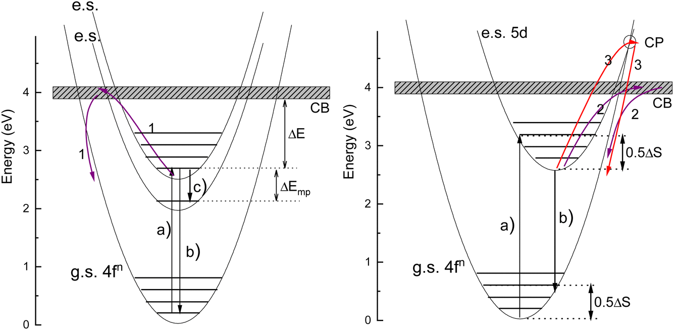 | ||
| Fig. 1 Illustration of the various quenching mechanisms in lanthanide luminescence. Arrows (1)–(3) in the two configurational coordinate diagrams illustrate the quenching of 4fn emission via the conduction band (CB), quenching of 5d emission via the CB, and quenching of 5d emission via the crossing point (CP), respectively. Arrow (c) in the left hand panel illustrates the quenching of 4f–4f emissions via multi-phonon relaxation to a ΔEmp lower lying excited state. The contributions to the Stokes shift ΔS from the excited and ground state relaxation for 5d–4f emissions are indicated in the right hand panel. The Stokes shift is negligible for 4f–4f transitions in the left hand panel. | ||
Fig. 2 shows the relevant 4fn levels of lanthanides Pr3+ (n = 2), Eu3+ (n = 6), and Tb3+ (n = 8). We will consider the thermal quenching of the luminescence from the 3P0 level of Pr3+, the 5D0 level of Eu3+, and the 5D4 level of Tb3+. Here, the energy gaps ΔEmp with the next lower 1D2, 7F6, and 7F0 4f levels are 0.5 eV, 1.55 eV, and 1.82 eV, respectively. Whenever the 5D4 or 3P0 level is close to the CB-bottom, quenching may proceed via the charge transfer state. This means that an electron is thermally excited from the emitting 4fn excited state to the conduction band (CB) of the host compound as illustrated with arrows (1) in Fig. 1. The energy difference ΔE between the location of the emitting state in the band gap and the CB-bottom is then the relevant quenching energy barrier. In the case of Pr3+, there is only 0.5 eV energy difference with the next lower 4f2 state and the quenching route via multi-phonon relaxation to 1D2 also need to be considered. Charge transfer quenching also applies to Eu3+, but instead of electron ionization to the CB quenching proceeds by hole ionization to the valence band (VB), i.e., Eu3+ (5D0) → Eu2+ (8S7/2) + VBh where a valence band hole (VBh) is created.
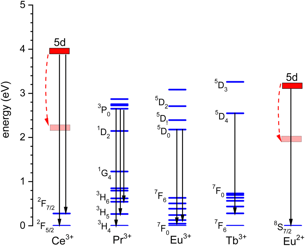 | ||
| Fig. 2 Relevant level energies and luminescence transitions of Ce3+, Pr3+, Eu3+, Tb3+, and Eu2+. The energy of the lowest 5d-level depends on the compound and the range is indicated by the curved dashed arrows. | ||
Ce3+ and Eu2+ show the dipole allowed 4fn−1 and 5d–4fn emissions. Different from exciting a 4fn state there will be significant lattice relaxation after exciting to a 4fn−15d-state. This leads to an offset in the configuration coordinate diagram as illustrated in Fig. 1. Thermal quenching may proceed via either electron ionizations to the CB illustrated by arrows (2) or alternatively when the CB is above the crossing point (CP) in the configurational coordinate diagram via that CP as illustrated by arrows (3) in Fig. 1.
In this work, we will focus on the quenching route via charge transfer to either the CB or the VB, and then the level locations of the emitting levels in the band gap need to be known in order to determine the quenching energy barrier ΔE. These level locations will be established with the (refined) chemical shift model developed in 2012 (and 2019).8–10 It makes use of the highly systematic changes in the level location with the number n of electrons in the 4fn-orbital of the lanthanides which is then combined with the spectroscopic data retrieved from the archival literature. It provides the so-called vacuum referred binding energy (VRBE) diagrams where all divalent and trivalent lanthanide ground and excited state levels are drawn with respect to the VB-top and CB-bottom and also with respect to the vacuum level. This work deals with about 170 different inorganic compounds, and for each compound the available spectroscopic data on the host and on divalent and trivalent lanthanides were gathered and combined to construct their VRBE diagrams. It is not doable to provide the references and analysis for each piece of data used (it would run into many 1000), and the reader has to trust that everything was performed with best scientific effort. Many VRBE schemes have already appeared in the literature where many references to the original data can be found. The reader may also conduct own search in the archival literature to derive, verify or improve the parameters used. The relevant parameters in the VRBE construction will be tabulated for each host and only the reference to information on the thermal quenching data will be provided.
A. Arrhenius equation, the chemical shift model and the VRBE scheme
The thermal quenching of luminescence intensity I(T) is traditionally expressed using the single barrier Arrhenius equation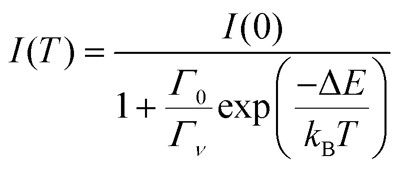 | (1) |
A similar equation applies for the lifetime τ(T) of the excited state
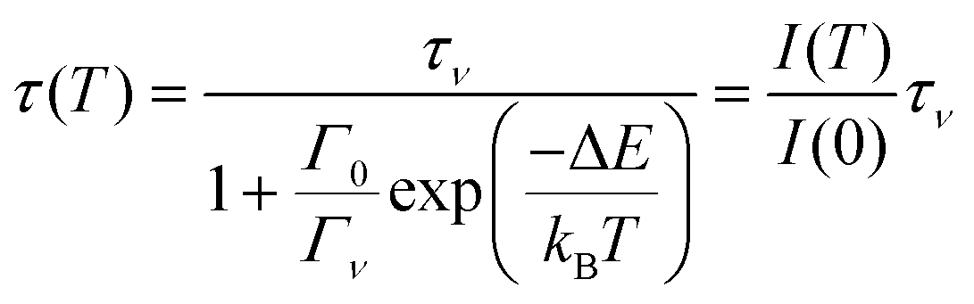 | (2) |
Depending on whether defects or dislocations happen to be nearby the activator or not, ΔE may change from activator to activator and therefore become spatial dependent. In cases where quenching proceeds by electron transfer to the CB or hole transfer to the VB, ΔE will also show a temperature dependence because the bandgap of the host compound will be temperature dependent. Due to lattice expansion when the temperature increases the (mobility) bandgap reduces typically by 0.05 eV per 100 K temperature increase. Therefore, the often made assumption of a temperature independent and a single value ΔE fails largely in practice. Furthermore, the radiative decay time usually shows a temperature dependence, i.e., it tends to increase with the temperature increase, see e.g. the quenching curves in ref. 11. Considering all the above, a single barrier Arrhenius fit to an experimental quenching curve will not provide good parameters for the activation energy and frequency factor. Instead of fitting, we will use a fixed value for Γ0 and estimate the average quenching energy barrier ΔE from the temperature where the luminescence intensity or decay has decreased by 10% (T10) or 50% (T50).
Using eqn (1) and (2), one obtains
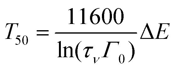 | (3) |
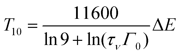 | (4) |
| A | Transition | λ (nm) | τ ν | T 50/ΔE (K eV−1) | T 10/ΔE (K eV−1) |
|---|---|---|---|---|---|
| Eu3+ | 5D0 → 7F1,2 | ≈610 | 2 ms | 475 | 435 |
| Tb3+ | 5D4 → 7F5 | ≈545 | 2 ms | 475 | 435 |
| Pr3+ | 3P0 → 3H4,5,6 | 490, 550, 620 | 50 μs | 560 | 510 |
| Eu2+ | 5d → 4f[8S7/2] | 380–600 | 1000 ns | 690 | 610 |
| Ce3+ | 5d → 4f[2 F5/2,7/2] | 300–550 | 40 ns | 850 | 735 |
B. Chemical shift model with the characteristic VRBE diagram
Fig. 3 shows the vacuum referred binding energy diagram for the lanthanides in YPO4 as constructed using the (Refined) Chemical Shift model. The model was first introduced in 20128 and refined later in 2019.9,10 The diagram shows the location of the divalent and trivalent ground states within the band gap and relative to the vacuum level. The vacuum referred binding energies are equivalent to the Ln3+/2+ and Ln4+/3+ charge transition levels. The most crucial parameter needed to construct a VRBE scheme is the U-value defined as the energy difference between the Eu3+/2+ and Eu4+/3+ CTLs which was determined as 7.09 eV for YPO4. The chemical shift model relates the U-value with the VRBEs of the Eu3+/2+ and Eu4+/3+ CTLs.8 The second parameter is the energy ECT for electron transfer from the valence band top to Eu3+ which when subtracted from the Eu3+/2+ CTL defines the VRBE EV at the VB-top. The third parameter is the energy Eex for the host exciton creation where we will always use the (estimated) value that pertains to a low temperature (≈10 K). When added to EV, it defines the VRBE EX of the electron in the exciton state. Bandgaps and exciton energies typically increase 0.05 eV at 100 K temperature lowering which means that a correction of about 0.15 eV is needed from the room temperature value. Finally, one needs to add the exciton electron hole binding energy Eeh to EX in order to reach the VRBE EC at the bottom of the CB. As a rule of thumb, we used Eeh = 0.008(Eex)2 as proposed in ref. 13. The CTLs for lanthanides other than Eu2+ and Eu3+ are then obtained by using the systematics in the shapes of the CTL curves (zig-zag curves) as treated in the Refined Chemical Shift model.9,10 The Dieke diagrams for the divalent and trivalent lanthanides are then used to determine the VRBE in the excited lanthanide states.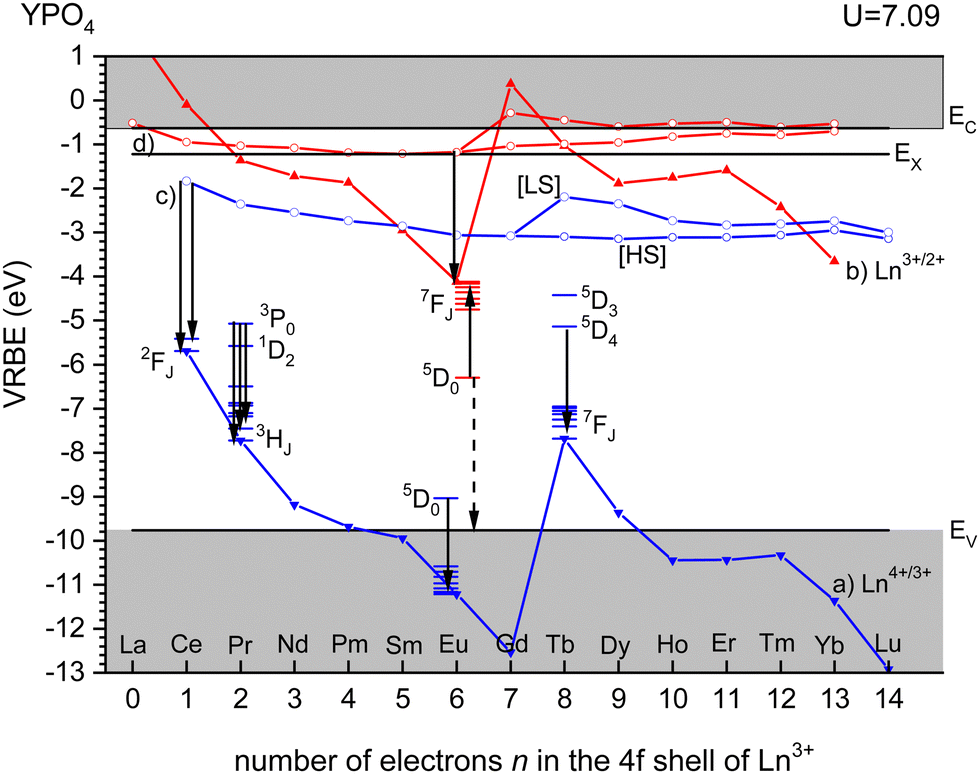 | ||
| Fig. 3 Vacuum referred binding energy scheme for the trivalent and divalent 4fn lanthanide ground state levels in YPO4. (a) Connects the VRBE in the Ln3+ 4fn ground state levels and can also be denoted as the Ln4+/3+ charge transition levels. (b) Connects the same for divalent lanthanides. (c) Connects the VRBE in the lowest energy 4fn−15d states of trivalent lanthanides where for n > 7 a distinction between the high spin [HS] and the low spin [LS] states is made. (d) Connects the same for divalent lanthanides. EV, EX, and EC are the VRBE at the valence band top, in the host exciton state, and at the conduction band bottom, respectively. | ||
Fig. 3 shows the 4f2, 4f6, and 4f8 level locations of Pr3+, Eu3+, and Tb3+ together with the 4fn–4fn luminescence transitions of relevance to this work indicated by the arrows. In the case of Eu3+, the levels and transition are shown with both the usual ‘electron picture’ and the less familiar ‘hole-picture’.14 The scheme shows that the lowest Eu2+ 5d state is close below the CB-bottom. The emitting 5d-state for Ce3+ is always further below. Note that the energy gap ΔEmp to the 2F7/2 level for Ce3+ and to the ground state of Eu2+ is several eV and multi-phonon relaxation is highly improbable. It is already well-established that the thermal quenching of these lanthanides usually proceeds by thermally activated electron transfer from the 5d-state to the conduction band, see Fig. 1.
For YPO4, the emitting 3P0 level of Pr3+ and the 5D4 level of Tb3+ appear at mid band gap near −5 eV VRBE. The energy difference with the CB-bottom is very large (>4 eV) and the thermal quenching of these emissions in YPO4 proceeds by other routes than via the CB. However, in compounds where the CB is located below, say, EC = −3 eV thermal quenching via the conduction band becomes important. Thermal ionization to the CB from the 5D0 level of Eu3+ will be impossible for all types of compounds. Instead, quenching takes place via the VB → Eu3+ charge transfer state which can be best visualized with the ‘hole picture’.14 Here, the ground state of Eu3+ is visualized as a hole trapped by Eu2+ which is then placed at the Eu3+/2+ CTL. Excitation of Eu3+ implies that the hole is excited downwards in the VRBE scheme. Thermal quenching can now proceed by ionization of the hole to the valence band illustrated by the dashed arrow. The quenching energy barrier ΔE is then the energy difference between the 5D0 level and EV.
II. Results
A. Thermal quenching of the Eu3+ 5D0 emission
Even at 1000 K, it is unlikely that the 5D0 → 7FJ luminescence transitions of Eu3+ will be quenched by multi-phonon relaxation. The energy difference of 1.55 eV with the next lower energy 7F6 level is just too large to bridge. Instead, quenching proceeds via the VB → Eu3+ charge transfer state. This implies that the excitation energy of the 5D0 level of about 2.18 eV together with the energy supplied from the thermal bath is converted into a state with a hole in the VB together with Eu2+ in its ground state. In the VRBE scheme, this is illustrated with the ‘hole picture’ where the 5D0 state is located 2.18 eV below the Eu3+/2+ CTL. Since the Eu3+/2+ CTL appears always near −4 eV, the quenching temperature will be directly linked to the VRBE EV at the VB-top, and one needs to lower the VB to increase thermal stability. The energies ECT at the maximum of the Eu3+ CT-band observed in the excitation spectra of the Eu3+ emission for several hundred different compounds were compiled in 2005.15 Since 2005, many more data or more accurate data have appeared and the values reported in the Tables to follow provide the, in the authors’ opinion, most likely values.A relationship between the Eu3+ luminescence quantum efficiency at room temperature and the energy ECT was established long time ago by Blasse.16 Later, Struck and Fonger17 studied the quenching as a function of temperature and explained it in terms of a configurational coordinate diagram involving the charge transfer state. In ref. 18, the data compiled on 12 different compounds revealed a linear relationship between ECT and T10 in a 0 to 800 K temperature range. Later, in ref. 13, 13 more compounds were added to the compilation. In ref. 14, the ‘hole picture’ was used to describe the quenching by hole ionization and a T10/ΔE of ≈ 430 K eV−1 relationship was found which agrees well with the prediction from eqn (4) as listed in Table 1.
In this work, we added new information. We selected compounds with a relatively low Eu3+ concentration (about 1%). Often, the data for decay time quenching were preferred over those of intensity quenching because the latter tend to be less accurate. The results are shown in Fig. 4 and the data and references are found in Table 2. We also added information on Eex and the U-values from which the data on EV and EC are obtained using the refined chemical shift model. The typical error bars are ±0.12 eV in the CT-energy and ±50 K in the T10 value. ΔE on the horizontal axis was obtained by
| ΔE = ECT − E(5D0) − 5 × 10⁻⁵T10Eex | (5) |
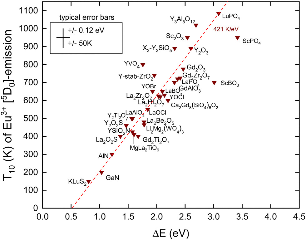 | ||
| Fig. 4 10% Quenching temperature T10 for the Eu3+ emission from the 5D0 level against the energy difference between the 5D0 hole state and the VB-top. The fitted dashed line has a slope of 421 K eV−1. | ||
| A | U | E CT | E V | E ex | E C | ΔE | T 10 | Ref. |
|---|---|---|---|---|---|---|---|---|
| LaOCl | 6.65 | 4.20 | −8.10 | 6.45 | −1.32 | 1.85 | 550 | 19 |
| YOCl | 6.65 | 4.54 | −8.44 | 7.10 | −0.94 | 2.14 | 630 | 20 |
| YOBr | 6.57 | 4.32 | −8.18 | 6.50 | −1.34 | 1.93 | 650 | 20 |
| LaPO4 | 7.18 | 4.84 | −9.00 | 8.10 | −0.38 | 2.37 | 720 | 7 |
| LuPO4 | 7.08 | 5.74 | −9.85 | 8.70 | −0.55 | 3.09 | 1085 | 7,21 |
| ScPO4 | 7.02 | 5.95 | −10.0 | 7.40 | −2.19 | 3.42 | 950 | 7,22 |
| LaBO3 | 6.93 | 4.51 | −8.54 | 7.05 | −1.10 | 2.10 | 650 | 23,24 |
| ScBO3 | 6.86 | 5.44 | −9.44 | 7.10 | −1.94 | 3.01 | 700 | 24 |
| Ca2Gd8(SiO4)6O2 | 6.80 | 4.59 | −8.56 | 7.00 | −1.17 | 2.20 | 600 | 7 |
| X2-Y2SiO5:(Ce1) | 6.86 | 4.80 | −8.80 | 6.82 | −1.61 | 2.32 | 890 | 7,25 |
| LaAlO3 | 6.76 | 3.91 | −7.86 | 6.10 | −1.47 | 1.58 | 500 | 26 |
| GdAlO3 | 6.75 | 4.75 | −8.70 | 7.36 | −0.90 | 2.31 | 700 | 4 |
| Y3Al5O12 | 6.77 | 5.23 | −9.19 | 7.10 | −1.69 | 2.69 | 1020 | 7 |
| Li2Mg2(WO4)3 | 7.15 | 4.07 | −8.21 | 4.70 | −3.34 | 1.78 | 465 | 27 |
| YVO4 | 6.80 | 4.10 | −8.07 | 4.00 | −3.94 | 1.76 | 800 | 7 |
| MgLa2TiO6 | 6.68 | 3.88 | −7.79 | 4.50 | −3.13 | 1.60 | 410 | 28 |
| Gd2Ti2O7 | 6.79 | 3.94 | −7.91 | 4.15 | −3.62 | 1.68 | 400 | 29 |
| Y2Ti2O7 | 6.79 | 3.85 | −7.82 | 4.25 | −3.42 | 1.56 | 500 | 2 |
| Zr0.83Y0.17O1.91 | 6.70 | 4.34 | −8.26 | 5.40 | −2.63 | 1.96 | 740 | 7,30 |
| La2Zr2O7 | 6.66 | 4.43 | −8.33 | 6.00 | −2.05 | 2.06 | 620 | 5,31 |
| La2Hf2O7 | 6.65 | 4.40 | −8.30 | 6.00 | −2.01 | 2.03 | 625 | 5,31 |
| La2Be2O5 | 6.70 | 4.11 | −8.03 | 6.28 | −1.44 | 1.78 | 480 | 32 |
| Gd2Zr2O7 | 6.65 | 4.81 | −8.71 | 6.00 | −2.42 | 2.41 | 725 | 6 |
| C-Gd2O3:(S6) | 6.60 | 4.86 | −8.74 | 5.50 | −2.99 | 2.47 | 775 | 33 |
| C-Y2O3:(S6) | 6.60 | 5.05 | −8.93 | 6.10 | −2.53 | 2.60 | 890 | 33,34 |
| C-Sc2O3:(C2) | 6.60 | 5.02 | −8.90 | 6.30 | −2.28 | 2.54 | 950 | 33 |
| La2O2S | 6.37 | 3.64 | −7.41 | 4.75 | −2.48 | 1.37 | 400 | 19,35 |
| Y2O2S | 6.37 | 3.76 | −7.53 | 4.85 | −2.49 | 1.47 | 460 | 19 |
| KLuS2 | 6.20 | 3.02 | −6.71 | 4.35 | −2.21 | 0.81 | 150 | 36 |
| YSiO2N | 6.70 | 3.89 | −7.81 | 6.10 | −1.41 | 1.58 | 425 | 37 |
| AlN-wurtzite | 6.40 | 3.49 | −7.27 | 6.20 | −0.76 | 1.22 | 300 | 38 |
| GaN-wurtzite | 6.40 | 3.25 | −7.03 | 3.48 | −3.45 | 1.04 | 200 | 38–40 |
There are few outliers notably ScBO3, ScPO4 and YVO4 as shown in Fig. 4. Disregarding these, a linear least square fit through the data yields the dashed line with a slope of 421 K eV−1 which agrees very good with a predicted value of 435 K eV−1 as shown in Table 1. The compound to compound variation in decay time, in maximum phonon frequencies, and in relaxation effects, and the experimental errors in ECT and T10 then provide the scatter of data.
Note that the fitted line does not cross the horizontal at zero energy but near 0.5 eV. We assumed that quenching occurs by the full ionization of the hole. However, this is not necessarily needed. The CT-state is a hole at the valence band that is still Coulomb bonded with the transferred electron, i.e., Eu2+, and radiation less recombination may start from this bonded state which will lower ΔE. Furthermore, 0.5 eV is of the same magnitude as the energy involved in lattice relaxation and Stokes shift.15,41 We therefore interpret the intercept near 0.5 eV as an effect of electron–hole bonding and lattice relaxation.
B. Thermal quenching of the Tb3+ 5D4 emission
The energy gap between the emitting 5D4 level of Tb3+ and the next lower 7F0 4f8-level is about 1.8 eV. This is even larger than that in the case of Eu3+ considered above, and multi-phonon relaxation is like for Eu3+ not a feasible quenching mechanism. Instead, in cases where the CB-bottom is not too far above the 5D4 level, thermal quenching can proceed by electron ionization to the CB. For YPO4 in Fig. 3 with the CB-bottom at −0.63 eV, the distance is 4.5 eV which is clearly too large. However, in transition metal based compounds like tantalates, tungstates, vanadates, niobates, molybdates and titanates, the CB-bottom appears at −3 eV to −4 eV.42 The excitation spectra of the Tb3+ emission in these compounds often reveal a so-called intervalence charge transfer (IVCT) band attributed to the excitation of an electron from the Tb3+ 7F6 ground state43,44 to the CB. Whereas the CT-band energy of Eu3+ provides the location of the Eu2+ ground state above the VB, the IVCT band provides the Tb3+ ground state below the CB. Therefore, the IVCT band energy determines the quenching energy barrier ΔE and therewith the quenching temperature T50. This was already demonstrated for Tb3+ in transition metal element based compounds in ref. 42. In ref. 14, compounds such as SnO2, Ga2O3, Lu2O3, and GaN with low lying conduction bands were added to the collection.IVCT bands are ≈0.8 eV broad and in many compounds they tend to overlap partly with the host excitation band. This introduces often larger errors in the derived value for the IVCT energy EIVCT(Tb3+). To improve accuracy, one may construct a VRBE diagram as shown in Fig. 3 that combines the spectroscopic data on many different lanthanides thus leading to more accurate ΔE values. This method was followed in ref. 14 and 42 where VRBE diagrams were constructed using the 2012 chemical shift model.8 We will adopt here the same method but now using the refined chemical shift model which provides few 0.1 eV different Tb4+/3+ CTL energies. The results are compiled in Table 3 and are shown in Fig. 5. Other than for Eu3+, there is no need to correct for bandgap lowering with the increase of temperature because we assume that the Tb3+ levels move down with the same pace as the downward movement of the CB-bottom.
| A | U | E CT | E V | E ex | E C | ΔE | T 50 | Ref. |
|---|---|---|---|---|---|---|---|---|
| SnO2 | 7.00 | 3.85 | −7.92 | 3.59 | −4.23 | 0.79 | 190 | 45 |
| CaSnO3 | 6.80 | 4.37 | −8.34 | 4.93 | −3.21 | 1.55 | 420 | 46 |
| β-Ga2O3 | 6.90 | 4.28 | −8.40 | 5.05 | −3.15 | 1.80 | 385 | 47 |
| CaMoO4 | 7.00 | 4.40 | −8.47 | 4.60 | −3.70 | 1.32 | 450 | 48 |
| KLa(MoO4)2 | 7.05 | 4.20 | −8.29 | 4.60 | −3.52 | 1.56 | 455 | 49 |
| KY(WO4)2 | 7.15 | 4.60 | −8.74 | 4.55 | −4.03 | 1.18 | 410 | 50 |
| KLu(WO4)2 | 7.15 | 4.55 | −8.69 | 4.50 | −4.03 | 1.18 | 325 | 51 |
| LaVO4 | 6.80 | 3.95 | −7.92 | 4.25 | −3.53 | 1.24 | 230 | 52 |
| GdVO4 | 6.84 | 4.05 | −8.04 | 4.00 | −3.91 | 0.90 | 140 | 53 |
| LuVO4 | 6.80 | 4.06 | −8.03 | 3.85 | −4.06 | 0.70 | 80 | 53 |
| LiNbO3 | 6.87 | 4.47 | −8.47 | 4.62 | −3.68 | 1.17 | 200 | 54,55 |
| CaNb2O6 | 6.85 | 4.10 | −8.10 | 4.75 | −3.16 | 1.66 | 490 | 56 |
| YNbO4 | 6.84 | 4.60 | −8.59 | 4.96 | −3.43 | 1.38 | 455 | 56 |
| LiTaO3 | 6.65 | 4.54 | −8.44 | 5.50 | −2.70 | 1.87 | 585 | 55 |
| M′-YTaO4 | 6.78 | 5.10 | −9.06 | 5.95 | −2.83 | 1.91 | 750 | 57 |
| C-Lu2O3:(C2) | 6.60 | 4.81 | −8.69 | 5.90 | −2.51 | 2.00 | 525 | 58 |
| Ga0.7Al0.3 N | 6.40 | 3.22 | −7.01 | 4.05 | −2.83 | 1.44 | 250 | 59 |
| GaN-wurtzite | 6.40 | 3.25 | −7.03 | 3.48 | −3.45 | 0.81 | 30 | 59–61 |
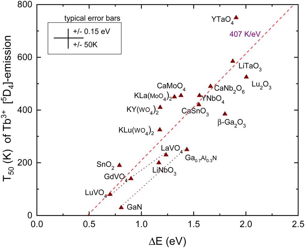 | ||
| Fig. 5 T 50 data for emission from the 5D4 level of Tb3+ in compounds against the energy difference ΔE between the 5D4 level and the CB-bottom. | ||
When assuming that the energy EIVCT at the maximum of the IVCT band locates the Tb3+ ground state below the CB-bottom, one obtains for ΔE
| ΔE = EIVCT(Tb3+) − E(5D4) | (6) |
When the quenching energy barrier is derived from the VRBE diagram construction one obtains for ΔE
| ΔE = [Eex + 0.008(Eex)2] − [ECT − U + ΔE(Eu, Tb) + E(5D4)] | (7) |
The dashed line in Fig. 5 is from a linear least squares fit through the data and has a slope of 407 K eV−1. This is somewhat smaller than the value of 475 K eV−1 predicted in Table 1. Nevertheless, a clear correspondence between the quenching temperature and the energy at the CB-bottom is evident. The situation and figure much resemble that of hole ionization in the case of Eu3+ as shown in Fig. 4. The similar lifetimes of 1–2 ms for Eu3+ and Tb3+ emissions result in similar slopes in the linear fits. Also, the intersection with the horizontal axis for both dopants occurs near 0.5 eV.
Note that the 5D3 level of Tb3+ is located 0.7 eV above the 5D4 level and therefore located 0.7 eV closer to the CB-bottom. Since the 5D3 and 5D4 lifetimes differ not too much (factor of 2), one may expect about 350 K lower thermal stability of the 5D3 emission. Indeed, the difference amounts 375 K for CaMoO463 and 370 K for CaNb2O6.56 Furthermore, whenever T50 (5D4) is < 300 K, the emission from 4D3 is absent even down to 4 K. This can be verified with the data compiled in ref. 42.
C. Thermal quenching of the Pr3+ 3P0 emission
The Pr4+/3+ CTL is near the same energy as that for Tb4+/3+. Also, the emitting 3P0 level of Pr3+ is near the same VRBE as that for the 5D4 level of Tb3+ as can be seen in the scheme for YPO4 in Fig. 3. This means that like for Tb3+ thermal quenching may proceed by electron ionization to the CB in compounds with the low lying CB-bottom. Other than Tb3+ and Eu3+, the next lower excited state (1D2) is only at ΔEmp = 0.5 eV lower energy. At a sufficiently high temperature, the multi-phonon relaxation to 1D2 then becomes also a possible quenching route. The radiative lifetime of the 3P0 state is usually between 10 and 50 μs and is therefore shorter than those of Eu3+ and Tb3+. This translates to a steeper T50/ΔE = 560 K eV−1 slope as shown in Table 1. In ref. 42, a relationship between T50 of the 3P0 emission and the energy of the IVCT band, or equivalently the energy distance from the CB-bottom, was already demonstrated. Since then, more data have become available. Here, we have re-analyzed everything with the refined chemical shift model. The results are shown in Fig. 6 and compiled in Table 4.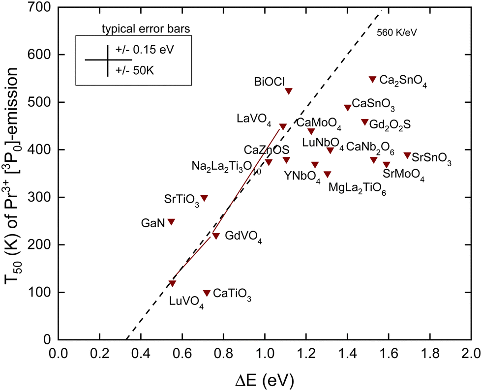 | ||
| Fig. 6 T 50 data for the emission from the 3P0 level of Pr3+ in compounds against the energy difference ΔE between the 3P0 level and the conduction band bottom. | ||
| A | U | E CT | E V | E ex | E C | ΔE | T 50 | Ref. |
|---|---|---|---|---|---|---|---|---|
| BiOCl | 6.70 | 3.55 | −7.47 | 4.00 | −3.34 | 1.12 | 525 | 64 |
| SrSnO3 | 6.96 | 4.00 | −8.05 | 4.70 | −3.17 | 1.69 | 390 | 65 |
| CaSnO3 | 6.80 | 4.37 | −8.34 | 4.93 | −3.21 | 1.40 | 490 | 65 |
| Ca2SnO4 | 6.85 | 4.43 | −8.42 | 5.05 | −3.17 | 1.52 | 550 | 65 |
| SrMoO4 | 7.05 | 4.25 | −8.34 | 4.75 | −3.41 | 1.59 | ≈370 | 66 |
| CaMoO4 | 7.00 | 4.40 | −8.47 | 4.60 | −3.70 | 1.23 | 440 | 67 |
| LaVO4 | 6.80 | 3.95 | −7.92 | 4.25 | −3.53 | 1.09 | 450 | 44 |
| GdVO4 | 6.84 | 4.05 | −8.04 | 4.00 | −3.91 | 0.76 | 220 | 53 |
| LuVO4 | 6.80 | 4.06 | −8.03 | 3.85 | −4.06 | 0.55 | 120 | 53 |
| CaNb2O6 | 6.85 | 4.10 | −8.10 | 4.75 | −3.16 | 1.53 | 380 | 56 |
| YNbO4 | 6.84 | 4.60 | −8.59 | 4.96 | −3.43 | 1.24 | 370 | 56 |
| LuNbO4 | 6.85 | 4.58 | −8.58 | 5.00 | −3.38 | 1.32 | 400 | 68 |
| SrTiO3 | 6.75 | 3.44 | −7.39 | 3.46 | −3.83 | 0.71 | ≈300 | 69,70 |
| CaTiO3 | 6.75 | 3.84 | −7.79 | 3.85 | −3.82 | 0.72 | ≈100 | 69,70 |
| Na2La2Ti3O10 | 6.75 | 3.70 | −7.65 | 4.00 | −3.52 | 1.02 | 375 | 71 |
| MgLa2TiO6 | 6.68 | 3.88 | −7.79 | 4.50 | −3.13 | 1.30 | 350 | 72 |
| CaZnOS | 6.35 | 3.73 | −7.49 | 4.51 | −2.82 | 1.11 | 380 | 73 |
| Gd2O2 S | 6.37 | 3.72 | −7.49 | 4.83 | −2.47 | 1.49 | 460 | 74 |
| GaN-wurtzite | 6.40 | 3.25 | −7.03 | 3.48 | −3.45 | 0.55 | 250 | 75,76 |
For the quenching energy barrier, we used the same method as for Tb3+. When assuming that the energy EIVCT(Pr3+) at the maximum of the IVCT band locates the Pr3+ ground state below the CB-bottom one obtains for ΔE
| ΔE = EIVCT(Pr3+) − E(3P0) | (8) |
When the quenching energy barrier is derived from the VRBE construction one obtains for ΔE
| ΔE = [Eex + 0.008(Eex)2] − [ECT − U + ΔE(Eu, Pr) + E(3P0)] | (9) |
The dashed line drawn through the data has a slope of 560 K eV−1 as predicted from Table 1. It crosses the horizontal axis near 0.3 eV which compares with that for Tb3+ and Eu3+ where the crossing was near 0.5 eV. The data seem initially to follow this slope, but when T50 approaches 400 K many data points start to level off. The mentioned multi-phonon relaxation to the 1D0 level may be responsible for this. A detailed analysis for each compound would be required to resolve this further. It is interesting to compare the results for the sequence of compounds LaVO4, GdVO4, and LuVO4 where the bottom of the CB-band is formed by the lowest 3d-orbitals of V4+.42 In this sequence, this CB-bottom lowers by about 0.5 eV, see column 6 in Tables 3 and 4. For both the Tb3+ 5D4 emission and the Pr3+ 3P0 emission, this leads to increasingly lower T50 as seen in Fig. 5 and 6.
The 1G4 level of Pr3+ is ΔEmp = 0.86 eV below the 1D2 level which makes multi-phonon relaxation from 1D2 less probable than that from the 3P0 level. The quenching of the 1D2 emission may again proceed via the CB. Although the lifetime of the 1D2 level is about 10 times longer than that of 3P0 its 0.5 eV further distance below the CB is more important leading to the significantly higher thermal stability of the 1D2 emission. The difference in T50 for CaNb2O6,56 LuNbO4,68 and MgLa2TiO672 appears about 200 K in line with the expectation.
D. Thermal quenching of the Eu2+ 4f6 5d–4f7 emission
Techniques such as photoconductivity, excited state absorption, delayed fluorescence, and thermoluminescence charging studies have evidenced that the quenching of the Eu2+ emission proceeds often, if not always, by means of the thermal ionization of the 5d electron to the CB. The consistency between quenching via the CB and Eu2+ level locations with respect to the CB-bottom was demonstrated in ref. 77. The same was concluded from first principles studies on fifteen representative Eu2+-doped phosphors by Jia et al.78The nature of the 5d–4f emission is much different from that of the 4fn–4fn emission. The transition is dipole allowed leading to much shorter radiative lifetimes. It varies for Eu2+ between 500 and 1500 ns79 and from eqn (3) we then expect T50 to change with about 690 K eV−1, see Table 1. A large amount of data on Eu spectroscopy have been compiled and many VRBE schemes like that of YPO4 in Fig. 3 have been constructed. These VRBE schemes provide us with information on the energy difference between the lowest energy 4fn−15d-level and the CB-bottom. However, there are multiple error sources in this method. We need the energy ECT of the Eu3+ CT-band to locate the VB-top below the Eu3+/2+ CTL. Next, we need the (estimated) energy Eex for the host exciton creation to estimate the CB-bottom above the VB-top. Finally, we need the energy Efd of the transition from the Eu2+ ground state to the lowest level of the 4f65d excited state. Each step may contribute to the uncertainty in the 5d to CB-bottom energy difference. Different from the 4fn–4fn emissions of Eu3+, Tb3+, and Pr3+ where the Stokes shift is negligible, we have to deal with the Stokes shift ΔS between 4f–5d absorption and the 5d–4f emission that may amount 0.15 eV to almost 1 eV.80
The T50 with eqn (1) and (2) should theoretically be the same. However, quite often, the quenching of the decay time occurs at a higher temperature than that of the intensity as is the case for Eu2+ in MSi2O2N2 (M = Ca, Sr, and Ba).81 Depending on the size of the Stokes shift, the emission band overlaps partly with the absorption bands which leads to the phenomenon of self-absorption. A photon emitted by one Eu2+ can be absorbed by another and then again be re-emitted. As a consequence, the decay time lengthens which increases T50,82 but since the luminescence quantum efficiency will be smaller than unity, the intensity decreases which lowers T50. The difference between decay derived T50 and intensity derived T50 may amount 100 K. In these cases, we used an average value for T50. The data on T50 are compiled in Table 5 together with the parameters used for the VRBE construction and ΔS.
| A | U | E CT | E V | E ex | E C | E fd | ΔS | ΔE | T 50 | Ref. |
|---|---|---|---|---|---|---|---|---|---|---|
| a For the alkaline halides, the spectroscopic data on ECT are not available. The values listed are the energy differences between the Eu3+/2+ CTLs and EV that was obtained directly from the published photoelectron spectroscopy data. | ||||||||||
| RbCla | 6.70 | 4.20 | −8.12 | 7.54 | −0.13 | 3.19 | 0.21 | 1.01 | 670 | 83 |
| KCla | 6.70 | 4.23 | −8.15 | 7.79 | 0.12 | 3.10 | 0.17 | 1.16 | 770 | 83 |
| NaCla | 6.70 | 4.48 | −8.40 | 7.96 | 0.06 | 3.02 | 0.12 | 1.15 | 850 | 83 |
| RbBra | 6.60 | 3.10 | −6.98 | 6.64 | 0.02 | 3.16 | 0.17 | 1.02 | 690 | 83 |
| KBra | 6.60 | 3.53 | −7.41 | 6.80 | −0.24 | 3.14 | 0.22 | 1.14 | 717 | 83 |
| NaBra | 6.60 | 3.40 | −7.28 | 6.75 | −0.16 | 3.02 | 0.13 | 0.96 | 740 | 83 |
| CsIa | 6.25 | 2.60 | −6.31 | 5.80 | −0.24 | 2.97 | 0.19 | 0.50 | 220 | 84 |
| KIa | 6.25 | 3.00 | −6.71 | 5.88 | −0.56 | 3.07 | 0.20 | 0.99 | 450 | 85 |
| Ba5(PO4)3Cl | 6.89 | 4.40 | −8.41 | 7.30 | −0.69 | 3.05 | 0.20 | 0.37 | 510 | 86,87 |
| Sr5(PO4)3Cl | 6.90 | 4.66 | −8.68 | 7.50 | −0.73 | 2.92 | 0.15 | 0.45 | 460 | 88 |
| Ca5(PO4)3Cl | 6.88 | 5.04 | −9.05 | 7.70 | −0.88 | 2.97 | 0.24 | 0.28 | 480 | 87,89 |
| Ca2BO3 Cl | 6.77 | 4.49 | −8.45 | 7.15 | −0.89 | 2.68 | 0.43 | 0.60 | 450 | 90 |
| Ca8Mg(SiO4)4Cl2 | 6.60 | 4.47 | −8.35 | 6.95 | −1.01 | 2.61 | 0.16 | 0.34 | 425 | 91 |
| α-Sr2P2O7 | 7.13 | 4.68 | −8.81 | 7.85 | −0.47 | 3.12 | 0.16 | 0.62 | 470 | 92 |
| LiSrPO4 | 7.05 | 4.77 | −8.86 | 7.75 | −0.63 | 2.95 | 0.20 | 0.61 | 450 | 93 |
| Ca10K(PO4)7 | 7.05 | 5.06 | −9.15 | 8.00 | −0.64 | 2.95 | 0.27 | 0.64 | 450 | 94 |
| NaCaPO4 | 7.07 | 4.77 | −8.87 | 7.75 | −0.64 | 2.77 | 0.31 | 0.85 | 600 | 95,96 |
| YPO4 | 7.09 | 5.65 | −9.77 | 8.55 | −0.63 | 2.94 | 0.04 | 0.57 | 230 | 97 |
| LuPO4 | 7.08 | 5.74 | −9.85 | 8.70 | −0.55 | 2.94 | 0.05 | 0.65 | 230 | 97 |
| BaB8O13 | 7.30 | 5.15 | −9.38 | 8.15 | −0.69 | 3.35 | 0.24 | 0.30 | 500 | 98,99 |
| SrB6O10 | 7.31 | 5.49 | −9.71 | 8.30 | −0.86 | 3.35 | 0.15 | 0.08 | 300 | 100 |
| Ba2Ca(BO3)2 | 6.93 | 4.61 | −8.64 | 6.90 | −1.36 | 2.79 | 0.38 | 0.07 | 190 | 101 |
| NaBa4(BO3)3 | 6.84 | 4.58 | −8.57 | 7.00 | −1.18 | 2.64 | 0.35 | 0.35 | 280 | 102 |
| NaSr4(BO3)3 | 6.85 | 4.65 | −8.64 | 7.20 | −1.03 | 2.67 | 0.69 | 0.64 | 370 | 102 |
| BaBPO5 | 7.24 | 4.81 | −9.00 | 8.53 | 0.12 | 3.42 | 0.16 | 0.97 | 565 | 103 |
| SrBPO5 | 7.22 | 4.96 | −9.14 | 8.53 | −0.03 | 3.49 | 0.29 | 0.80 | 450 | 103 |
| α-CaAl2B2O7 | 7.03 | 4.96 | −9.04 | 7.30 | −1.32 | 3.06 | 0.18 | −0.21 | 60 | 104 |
| CaBPO5 | 7.22 | 5.06 | −9.24 | 8.55 | −0.11 | 3.31 | 0.23 | 0.88 | 265 | 103 |
| α-SrSiO3 | 6.63 | 5.04 | −8.93 | 7.70 | −0.76 | 3.02 | 0.21 | 0.21 | 130 | 105 |
| CaMgSi2O6 | 7.03 | 5.10 | −9.18 | 7.95 | −0.73 | 2.97 | 0.20 | 0.49 | 390 | 106 |
| Ba2MgSi2O7 | 6.95 | 4.34 | −8.38 | 7.00 | −0.99 | 2.84 | 0.37 | 0.40 | 460 | 107,108 |
| Sr2MgSi2O7 | 7.03 | 4.75 | −8.83 | 7.29 | −1.12 | 2.82 | 0.19 | 0.24 | 250 | 109,110 |
| BaCa2Mg(SiO4)2 | 6.90 | 4.20 | −8.22 | 7.85 | 0.12 | 3.31 | 0.42 | 1.05 | 530 | 111,112 |
| Ba2SiO4 | 6.87 | 4.35 | −8.36 | 7.05 | −0.91 | 2.70 | 0.24 | 0.52 | 420 | 113–115 |
| Sr3 Mg(SiO4)2 | 6.91 | 4.54 | −8.57 | 7.45 | −0.67 | 3.02 | 0.32 | 0.49 | 515 | 116 |
| Sr2SiO4 | 6.81 | 4.64 | −8.61 | 7.20 | −1.00 | 3.19 | 0.55 | 0.07 | 425 | 117 |
| Li2SrSiO4 | 6.91 | 4.81 | −8.83 | 7.12 | −1.30 | 2.43 | 0.26 | 0.42 | 525 | 118 |
| CaAl2(SiO4)2 | 6.95 | 4.44 | −8.48 | 7.50 | −0.53 | 3.08 | 0.19 | 0.53 | 480 | 119 |
| Ca3Mg(SiO4)2 | 6.86 | 4.96 | −8.96 | 7.60 | −0.90 | 3.02 | 0.41 | 0.28 | 435 | 116,120 |
| β-Ca2SiO4 | 6.80 | 4.77 | −8.74 | 7.25 | −1.07 | 2.86 | 0.41 | 0.24 | 390 | 107 |
| Li2CaSiO4 | 6.92 | 4.77 | −8.80 | 7.55 | −0.79 | 2.73 | 0.14 | 0.58 | 450 | 121 |
| Sr3SiO5 | 6.74 | 4.07 | −8.01 | 6.50 | −1.17 | 2.43 | 0.29 | 0.48 | 485 | 122 |
| BaAl2O4 | 6.82 | 4.63 | −8.61 | 7.20 | −1.00 | 2.92 | 0.44 | 0.29 | 270 | 123,124 |
| Sr2Al(AlSiO7) | 6.82 | 4.79 | −8.77 | 7.50 | −0.82 | 2.88 | 0.23 | 0.39 | 300 | 125 |
| SrAl12O19 | 7.06 | 4.75 | −8.85 | 8.00 | −0.33 | 3.54 | 0.43 | 0.43 | 375 | 126 |
| SrAl4O7 | 6.89 | 5.02 | −9.03 | 8.00 | −0.52 | 3.10 | 0.47 | 0.63 | 260 | 126 |
| SrAl2O4:(site 2) | 6.80 | 4.55 | −8.52 | 6.85 | −1.30 | 3.06 | 0.28 | −0.25 | 210 | 127,128 |
| SrAl2O4:(site 3) | 6.80 | 4.19 | −8.16 | 6.85 | −0.94 | 2.76 | 0.37 | 0.46 | 420 | 127,128 |
| Sr4Al14O25:[HE-site] | 7.10 | 4.77 | −8.89 | 7.70 | −0.72 | 3.49 | 0.44 | 0.13 | 400 | 129 |
| Sr4Al14O25:[LE-site] | 6.85 | 4.77 | −8.77 | 7.70 | −0.59 | 2.82 | 0.30 | 0.73 | 380 | 129 |
| Ca2Al(AlSiO7) | 6.83 | 4.98 | −8.97 | 7.60 | −0.90 | 2.58 | 0.24 | 0.62 | 340 | 130,131 |
| CaAl2O4 | 6.80 | 4.73 | −8.70 | 7.40 | −0.86 | 3.14 | 0.32 | 0.13 | 320 | 132,133 |
| CaO | 6.31 | 4.88 | −8.62 | 6.94 | −1.30 | 1.89 | 0.21 | 0.66 | 250 | 134 |
| Ca2SiS4 | 6.40 | 2.06 | −5.84 | 5.00 | −0.64 | 2.38 | 0.18 | 0.85 | 445 | 135 |
| SrGa2S4 | 6.30 | 1.87 | −5.61 | 4.77 | −0.65 | 2.55 | 0.23 | 0.65 | 470 | 136,137 |
| CaGa2S4 | 6.25 | 1.90 | −5.61 | 4.52 | −0.93 | 2.36 | 0.14 | 0.49 | 450 | 138 |
| CaS | 6.17 | 2.35 | −6.03 | 4.70 | −1.15 | 2.07 | 0.16 | 0.54 | 475 | 139 |
| SrSi2O2N2 | 6.70 | 3.44 | −7.36 | 6.35 | −0.69 | 2.51 | 0.21 | 0.83 | 600 | 81 |
| SrSi2AlO2N3 | 6.60 | 2.97 | −6.85 | 5.60 | −0.99 | 2.73 | 0.23 | 0.27 | 450 | 140 |
| CaSi2O2N2 | 6.70 | 3.10 | −7.02 | 6.30 | −0.41 | 2.56 | 0.33 | 1.13 | 455 | 81 |
| Sr2Si5N8 | 6.33 | 2.56 | −6.31 | 5.00 | −1.11 | 2.19 | 0.18 | 0.53 | 550 | 141 |
| Ca2Si5N8 | 6.35 | 2.93 | −6.69 | 5.15 | −1.33 | 2.27 | 0.21 | 0.26 | 370 | 142 |
| CaAlSiN3 | 6.22 | 2.64 | −6.34 | 5.05 | −1.09 | 2.14 | 0.23 | 0.59 | 640 | 143,144 |
| SrMg2Al2N4 | 6.15 | 2.21 | −5.88 | 4.10 | −1.64 | 2.13 | 0.12 | −0.05 | 290 | 145 |
As illustrated in the configurational diagram of Fig. 1, the excited state, after lattice relaxation, is lowered by 0.5ΔS and the emission ends (arrow b) at 0.5ΔS above the relaxed ground state leading to the overall Stokes shift ΔS. It is not established yet how the lattice relaxation affects the VRBE in the 5d-state but we assumed that 0.5ΔS is also a measure for the lowering in the VRBE. A correction of 0.5ΔS was made to obtain ΔE values in Table 5. Only the references for the quenching temperature are provided.
The used expression for ΔE is therefore
| ΔE = [Eex + 0.008(Eex)2] − [ECT + EEufd − 0.5ΔS] | (10) |
Fig. 7 shows all the data on T50 for the Eu2+ 5d–4f emission derived from the luminescence intensity or decay time quenching. The dashed line through the data was constructed with a predicted slope of 690 K eV−1 in Table 1. The first inspection reveals a scattered collection of data where T50 shows a tendency to increase with ΔE. However, a least square fitted line through the data has a slope of 310 K eV−1 which is much smaller than the anticipated 690 K eV−1 value. Even when the outlier data points for CaSi2O2N2, SrAl2O4, and CaBPO5 are ignored still, a too low slope of 360 K eV−1 is obtained. Considering all error sources, the large scatter in data is not unexpected. In constructing VRBE schemes, it is always assumed that the energy at the maximum of the Eu3+ CT band locates the VB-top below the Eu3+/2+ CTL.41 However, it is not guaranteed that this applies to the entire family of inorganic compounds. Perhaps for oxides the assumption works quite well, whereas for wide band gap fluorides or small band gap sulfides the assumption may lead to a systematic over-estimation or under-estimation of the VB to the CTL energy difference which will reflect in the derived value for ΔE. The under- or over-estimation can be at most few 0.1 eV; otherwise, EV will not be consistent anymore with the values derived from alternative methods such as photoelectron spectroscopy, computational methods, and electrochemical methods. Actually, for various small band gap compounds, the VRBE scheme places the lowest 5d-level above EC leading to the negative ΔE. Yet, 5d–4f luminescence is observed. This may indicate that for small band compounds the CT-maximum over-estimates the genuine Eu2+ to the VB energy difference. At this stage, it is, however, too early to enter further into this matter.
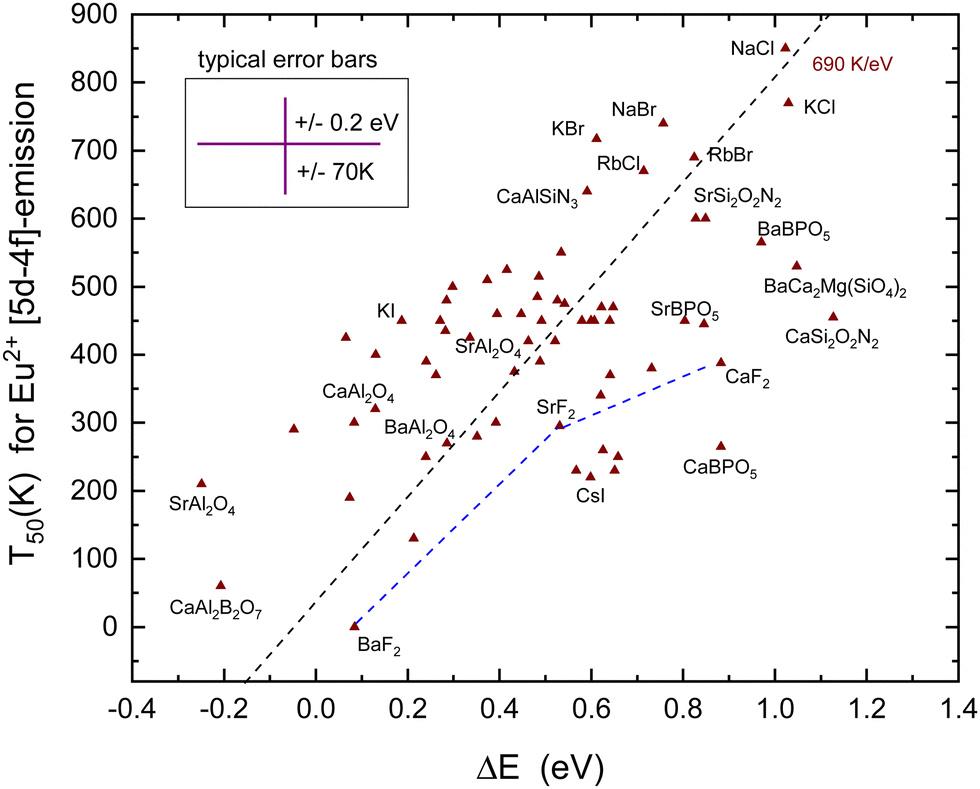 | ||
| Fig. 7 T 50 quenching data of the Eu2+ 5d–4f emission against the energy difference ΔE between the relaxed 5d-state and the CB-bottom. Data points for MF2 (M = Ba, Sr, Ca) compounds are connected by straight line segments. The typical error bars are shown. | ||
Despite the large scatter in data points, the results in Fig. 7 are consistent with the methods of the VRBE diagram construction and the errors therein. Note that almost all compounds in Table 5 concern Eu2+ on monovalent or divalent cation sites with the CB VRBE around or above −1 eV. Compounds with trivalent or higher valent cation sites for Eu2+ usually show a lower VRBE at the CB-bottom as can be verified for the compounds in Table 2–4, and vida infraTable 6. With few exceptions, in all these compounds, ΔE is negative and the Eu2+ emission is not observed.
E. Thermal quenching of the Ce3+ 5d–4f emission
Fig. 3 shows that for YPO4 the VRBE in the emitting 5d level of Ce3+ is about 0.6 eV below that of Eu2+. This energy difference is typical for almost all compounds, and such an energy difference will imply a higher quenching temperature T50 for Ce. The lifetime of the Ce3+ 5d–4f emission varies between 15 ns and 65 ns79 which is about 25 times shorter than that of Eu2+. This leads to the T50/ΔE = 850 K eV−1 rate in Table 1.For the study of the quenching of the Ce3+ 5d–4f emission, the same method as for the quenching of the Eu2+ emission was adopted, and the used expression for ΔE is
| ΔE = [Eex + 0.008(Eex)2] − [ECT − U + ΔE(Eu, Ce) + ECefd − 0.5ΔS] | (11) |
| A | U | E CT | E V | E ex | E C | E fd | ΔS | ΔE | T 50 | Ref. |
|---|---|---|---|---|---|---|---|---|---|---|
| BaF2 | 7.38 | 7.67 | −11.9 | 10.10 | −1.02 | 4.25 | 0.19 | 1.01 | 400 | 146–148 |
| SrF2 | 7.32 | 7.90 | −12.1 | 10.60 | −0.64 | 4.17 | 0.15 | 1.36 | 490 | 146 |
| CaF2 | 7.31 | 8.21 | −12.4 | 11.10 | −0.35 | 4.04 | 0.09 | 1.73 | 620 | 11 |
| LaF3 | 7.51 | 7.43 | −11.8 | 10.45 | −0.44 | 4.98 | 0.64 | 1.29 | 450 | 11 |
| LiYF4 | 7.52 | 8.09 | −12.4 | 11.00 | −0.46 | 4.32 | 0.19 | 1.72 | 1025 | 11 |
| LaBr3 | 6.60 | 2.00 | −5.87 | 5.40 | −0.24 | 4.07 | 0.54 | 0.94 | 750 | 149 |
| YI3 | 6.29 | 1.48 | −5.21 | 4.45 | −0.60 | 3.07 | 0.60 | 1.14 | 650 | 150 |
| Sr3(Al2O5)Cl2 | 6.77 | 4.51 | −8.47 | 6.70 | −1.41 | 3.70 | 0.75 | 0.51 | 525 | 151 |
| LaOBr | 6.58 | 4.11 | −7.98 | 6.25 | −1.41 | 3.47 | 0.43 | 0.28 | 300 | 152,153 |
| GdOBr | 6.56 | 4.24 | −8.10 | 6.40 | −1.37 | 3.34 | 0.26 | 0.34 | 450 | 153 |
| LaP3O9 | 7.26 | 5.84 | −10.0 | 8.45 | −1.02 | 4.28 | 0.21 | 0.80 | 690 | 154 |
| LiYP4O12 | 7.26 | 6.17 | −10.4 | 8.63 | −1.15 | 4.19 | 0.21 | 0.77 | 700 | 155 |
| YPO4 | 7.09 | 5.65 | −9.77 | 8.55 | −0.63 | 3.85 | 0.13 | 1.32 | 725 | 156 |
| Ca9Y(PO4)7 | 7.08 | 4.86 | −8.97 | 7.40 | −1.13 | 4.31 | 0.68 | 0.62 | 600 | 157 |
| Ba2Ca(BO3)2 | 6.90 | 4.61 | −8.63 | 6.90 | −1.35 | 3.14 | 0.49 | 1.20 | 550 | 158 |
| LiSr4(BO3)3 | 6.89 | 4.66 | −8.67 | 7.04 | −1.24 | 3.73 | 0.75 | 0.82 | 525 | 159 |
| Li6Gd(BO3)3 | 6.98 | 4.88 | −8.94 | 7.10 | −1.44 | 3.59 | 0.36 | 0.71 | 310 | 160,161 |
| Li6Y(BO3)3 | 6.98 | 4.98 | −9.04 | 7.20 | −1.42 | 3.58 | 0.39 | 0.75 | 440 | 162 |
| La2Si2O7 | 6.95 | 5.54 | −9.58 | 7.45 | −1.69 | 3.79 | 0.29 | 0.18 | 625 | 163 |
| Gd2Si2O7 | 6.64 | 4.92 | −8.81 | 7.20 | −1.20 | 3.53 | 0.38 | 0.50 | 520 | 164,165 |
| Lu2Si2O7 | 7.01 | 5.50 | −9.57 | 7.30 | −1.85 | 3.54 | 0.29 | 0.36 | 500 | 166–168 |
| CaAl2(SiO4)2 | 6.95 | 4.44 | −8.48 | 7.50 | −0.53 | 4.22 | 0.43 | 0.98 | 635 | 169 |
| LiYSiO4 | 6.89 | 5.51 | −9.52 | 7.55 | −1.52 | 3.55 | 0.44 | 0.57 | 600 | 170 |
| Ca3Sc2Si3O12 | 6.85 | 5.15 | −9.14 | 7.20 | −1.53 | 2.77 | 0.34 | 1.24 | 1150 | 171,172 |
| LaBO(SiO4) | 7.03 | 4.84 | −8.92 | 7.80 | −0.64 | 4.34 | 0.46 | 0.90 | 600 | 173 |
| La5 (SiO4)2BO4O | 6.84 | 4.38 | −8.37 | 6.70 | −1.31 | 3.57 | 0.59 | 0.76 | 395 | 174 |
| X1-Gd2SiO5:(Ce1) | 6.85 | 4.90 | −8.90 | 6.80 | −1.73 | 3.61 | 0.70 | 0.37 | 350 | 175,176 |
| X1-Gd2SiO5:(Ce2) | 6.85 | 4.90 | −8.90 | 6.80 | −1.73 | 3.32 | 0.69 | 0.67 | 250 | 175,176 |
| X2-Y2SiO5:(Ce1) | 6.86 | 4.80 | −8.80 | 6.82 | −1.61 | 3.45 | 0.31 | 0.47 | 440 | 177,178 |
| X2-Y2SiO5:(Ce2) | 6.80 | 4.81 | −8.78 | 6.82 | −1.59 | 3.25 | 0.67 | 0.78 | 410 | 178 |
| X2-Lu2SiO5:(Ce1) | 6.83 | 5.15 | −9.14 | 6.85 | −1.91 | 3.46 | 0.31 | 0.11 | 350 | 178,179 |
| X2-Lu2SiO5:(Ce2) | 6.83 | 5.15 | −9.14 | 6.85 | −1.91 | 3.36 | 0.68 | 0.40 | 290 | 178,179 |
| Sr3Y2Ge3O12 | 6.85 | 4.43 | −8.43 | 5.96 | −2.18 | 2.86 | 0.38 | 0.51 | 300 | 172,180 |
| Ca3Y2Ge3O12 | 6.85 | 4.77 | −8.77 | 6.20 | −2.26 | 2.92 | 0.36 | 0.37 | 265 | 180 |
| Mg3Y2Ge3O12 | 6.90 | 4.70 | −8.72 | 6.00 | −2.43 | 2.59 | 0.40 | 0.61 | 300 | 181 |
| Sr2 Al(AlSiO7) | 6.82 | 4.79 | −8.77 | 7.50 | −0.82 | 3.69 | 0.25 | 0.94 | 500 | 182 |
| Ca2 Al(AlSiO7) | 6.83 | 4.98 | −8.97 | 7.60 | −0.90 | 3.48 | 0.30 | 1.09 | 570 | 182 |
| Gd3Al5O12 | 6.84 | 5.39 | −9.38 | 6.55 | −2.49 | 2.64 | 0.42 | 0.43 | 400 | 183,184 |
| GdAlO3 | 6.75 | 4.75 | −8.70 | 7.36 | −0.90 | 4.09 | 0.37 | 0.41 | 345 | 185 |
| Y4Al2O9 | 6.75 | 5.19 | −9.13 | 6.45 | −2.35 | 3.18 | 0.35 | −0.14 | 60 | 186 |
| Y3Al5O12 | 6.77 | 5.23 | −9.19 | 7.10 | −1.69 | 2.71 | 0.33 | 1.01 | 645 | 11,187,188 |
| Y3Sc2Al3O12 | 6.56 | 5.28 | −9.14 | 6.90 | −1.86 | 2.86 | 0.48 | 0.44 | 530 | 189 |
| YAlO3 | 6.81 | 5.06 | −9.04 | 8.00 | −0.52 | 4.09 | 0.54 | 0.96 | 660 | 11,190 |
| LuAlO3 | 6.83 | 5.30 | −9.29 | 8.35 | −0.38 | 4.03 | 0.51 | 1.18 | 850 | 190 |
| Ca2 Ga(GaSiO7) | 6.95 | 4.48 | −8.52 | 5.85 | −2.40 | 3.54 | 0.49 | −0.18 | 450 | 191 |
| Gd3Ga1Al4O12 | 6.84 | 5.37 | −9.36 | 6.50 | −2.52 | 2.75 | 0.45 | 0.30 | 405 | 192,193 |
| Gd3Ga2Al3O12 | 6.86 | 5.28 | −9.28 | 6.36 | −2.59 | 2.81 | 0.47 | 0.21 | 405 | 192,193 |
| Gd3Ga3Al2O12 | 6.86 | 5.21 | −9.21 | 6.29 | −2.60 | 2.81 | 0.48 | 0.20 | 310 | 183,194,195 |
| Gd3Ga4Al1O12 | 6.88 | 5.00 | −9.01 | 6.07 | −2.65 | 2.88 | 0.49 | 0.12 | 150 | 193 |
| Y3Al4GaO12 | 6.77 | 5.21 | −9.17 | 7.10 | −1.66 | 2.78 | 0.36 | 0.98 | 605 | 192,196 |
| Y3Al3Ga2O12 | 6.77 | 5.23 | −9.19 | 6.93 | −1.87 | 2.83 | 0.32 | 0.70 | 525 | 192,196 |
| Y3Al2Ga3O12 | 6.77 | 5.19 | −9.14 | 6.52 | −2.28 | 2.85 | 0.39 | 0.30 | 380 | 192,196 |
| Y3AlGa4O12 | 6.80 | 5.12 | −9.09 | 6.44 | −2.32 | 2.93 | 0.45 | 0.26 | 275 | 192,196 |
| Y3Ga5O12 | 6.85 | 5.05 | −9.05 | 6.10 | −2.65 | 2.90 | 0.35 | −0.01 | 100 | 197,198 |
| SrHfO3 | 6.62 | 4.40 | −8.28 | 6.35 | −1.61 | 4.07 | 0.84 | −0.25 | 285 | 199 |
| CaHfO3 | 6.64 | 4.51 | −8.40 | 6.95 | −1.07 | 3.71 | 0.77 | 0.65 | 360 | 200 |
| LaLuO3 | 6.58 | 4.25 | −8.11 | 6.35 | −1.44 | 3.71 | 0.99 | 0.29 | 339 | 200 |
| LaScO3 | 6.66 | 4.20 | −8.10 | 6.20 | −1.60 | 3.85 | 0.80 | 0.03 | 255 | 200 |
| La2Be2O5 | 6.70 | 4.11 | −8.03 | 6.28 | −1.44 | 3.64 | 0.85 | 0.49 | 360 | 32 |
| GdScO3 | 6.70 | 4.73 | −8.65 | 6.10 | −2.25 | 3.59 | 0.74 | −0.34 | 232 | 200 |
| CaSc2O4 | 6.65 | 4.35 | −8.25 | 6.35 | −1.58 | 2.76 | 0.32 | 0.88 | 530 | 201,202 |
| Y2O2S | 6.37 | 3.76 | −7.53 | 4.85 | −2.49 | 2.68 | 0.65 | −0.21 | 63 | 203 |
| CaGa2S4 | 6.25 | 1.90 | −5.61 | 4.52 | −0.93 | 2.92 | 0.26 | 0.74 | 575 | 204 |
| LaSiO2N | 6.65 | 3.43 | −7.33 | 5.65 | −1.42 | 3.50 | 0.32 | 0.29 | 275 | 205 |
| SrAlSi4N7 | 6.40 | 2.88 | −6.66 | 5.05 | −1.41 | 2.80 | 0.42 | 0.69 | 525 | 206 |
| La3Si6N11 | 6.50 | 3.04 | −6.87 | 4.60 | −2.10 | 2.72 | 0.36 | 0.19 | 525 | 207 |
| LaSi3N5 | 6.48 | 2.58 | −6.40 | 4.85 | −1.36 | 3.56 | 0.55 | 0.15 | 550 | 208 |
For Eu2+, the used value for the parameter U was not of relevance for obtaining the quenching energy barrier. However, for Ce3+, it will be and this adds additional uncertainty to ΔE as derived from the VRBE scheme. The T50 values with references and the parameters used in the VRBE construction are compiled in Table 6.
The T50 and derived quenching energy barriers ΔE are shown in Fig. 8. The data appear to scatter like those for Eu2+ obscuring a clear relationship between the quenching temperature T50 and the quenching energy barrier ΔE. The dashed line with a slope of 850 K eV−1 is the predicted relationship shown in Table 1, whereas a linear fit provides only a slope of 325 K eV−1. One might argue that for thermal quenching the electron need not to reach the CB-bottom but it may quench via CB-derived states that are still bonded to Ce4+. The VRBE is then expected between EX and EC leading to a lowering of ΔE. It will shift and move around the data points several 0.1 eV but the general picture remains the same.
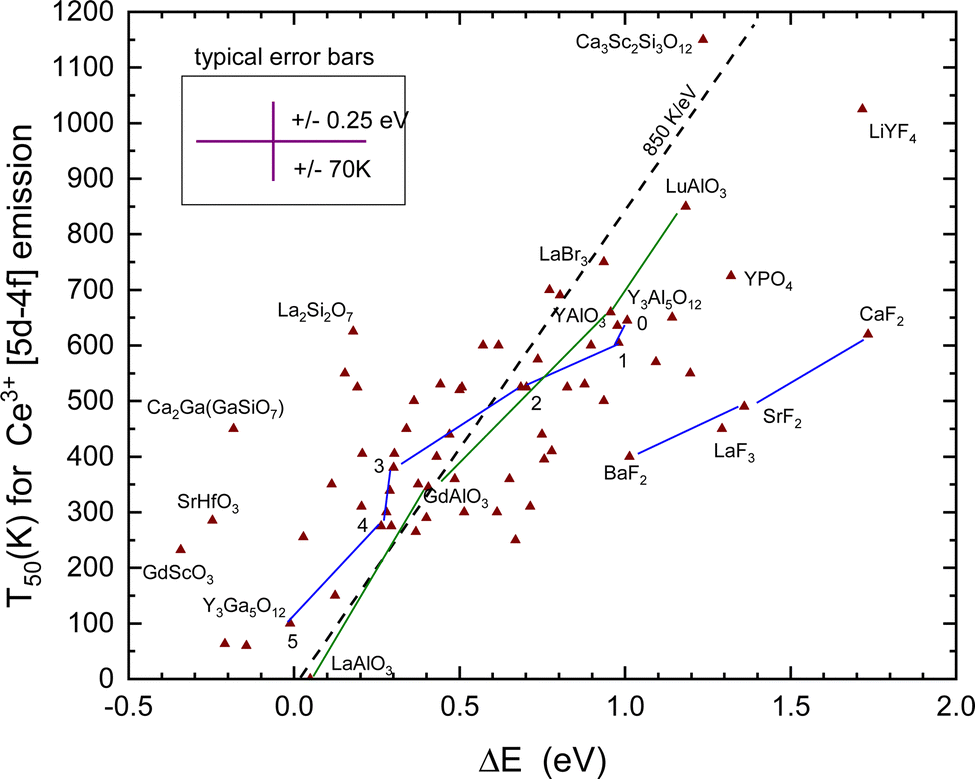 | ||
| Fig. 8 T 50 quenching data of the Ce3+ 5d–4f emission against the energy difference ΔE between the relaxed 5d-state and the CB-bottom. The typical error bars are shown. Data points for the sequence of compounds Y3Al5−xGaxO12 and REAlO3 (RE = La, Gd, Y, Lu) are connected by straight line segments. | ||
When we deal with a sequence of similar type of compounds systematic errors will drop out yielding better correspondence with the 850 K eV−1 prediction. One such sequence is BaF2, SrF2, and CaF2, where for both Eu2+ and Ce3+ the quenching temperature increases in accordance with the VRBE prediction. Furthermore, Ce3+ quenches at about 210 K higher temperature as Eu2+ also in accordance with the VRBE schemes. However, the data are located at about 0.5 eV too high ΔE values with respect to the data on other compounds. The reason is not known but it may indicate systematic errors in the VRBE-diagram construction. Another well-studied sequence is the Ce3+ doped Y3Al5−xGaxO12 and Gd3Al5−xGaxO12 garnet compounds. For the sequence x = 0, 1, 2, 3, 4, and 5, the data points for Y3Al5−xGaxO12 in Fig. 8 have been connected with straight line segments. These data appear to follow the steeper slope of 850 K eV−1 much better. The same applies for the sequence REAlO3 (RE = La, Gd, Y, and Lu). Ce3+ does not emit in LaAlO3 and we assumed a ΔS = 0.4 eV to place the data point in Fig. 8. For LuAlO3, we assumed T50 ≈ 850 K based on the work of ref. 190. Note that in the review work by Ueda and Tanabe209 on Ce3+ doped garnet compounds the quenching data followed a slope of 620 K eV−1.
Like for Eu2+, there is an entire class of materials with a low lying CB-bottom and then the emitting 5d-level of Ce3+ is above the CB-bottom. Emission is then not observed even down to 0 K. This applies to all compounds in Tables 3 and 4.
III. Discussion
The common aspect of the luminescence quenching of all five lanthanides considered in this work is that it proceeds via charge carrier transfer to the CB or the VB, and the energy difference ΔE between the emitting level and the host band is the most relevant parameter. In this work, this value is derived from the constructed VRBE schemes. Table 1 shows the predicted relationship between T50 and ΔE where a typical value for the vibrational frequency and the luminescence lifetime was assumed. A compound to compound variation in these values is unavoidable, and this will lead to the data scatter around the predicted relationships. The data for Eu3+ in Fig. 4 follow the predicted slope of 435 K eV−1 suprisingly closely. The error in ΔE is relatively small because only the error in ECT provides a dominant contribution, see eqn (5). For Tb3+ and Pr3+ in Fig. 5 and Fig. 6, ΔE is either based on the energy at the maximum of the IVCT band, see eqn (6) and (8), which usually overlaps partly with the host excitation band preventing accurate determination. The IVCT data together with the data from other lanthanides can also be used to construct VRBE schemes. Eqn (7) and (9) can then be used to determine ΔE. For both methods, the error in ΔE and the scatter in data appears larger than that for Eu3+; yet, the data show consistency with the predicted slopes of 475 K eV−1 and 560 K eV−1. For Pr3+, it was suggested that above 400 K multi-phonon relaxation to the lower lying 1D2 level becomes the dominant quenching route which then causes the data to deviate from the predicted trend.Errors and resulting scatter of data become larger for the 5d–4f emitters Eu2+ and Ce3+ in Fig. 7 and 8. For Eu2+ errors in ECT, Eex, and exciton binding energy, all add to the error in EC and therewith ΔE, see eqn (10) and (11). A standard random error of ±0.2–03 eV is estimated. In addition, there may be a systematic error related to the entire method of the VRBE construction. Particularly, the assumption that the energy at the maximum of the Eu3+ charge transfer band is always equal to the energy difference between the VB-top and the Eu3+/2+ CTL might not apply for all compounds alike.41 In a sense, the scatter of data provides insight into how accurate one can/should interpret the constructed VRBE schemes using the (refined) chemical shift model. Clearly, VRBE schemes are at this stage not accurate enough to predict the T50 values beforehand with a ±200 K accuracy.
To derive ΔE for Ce3+ requires in addition to ECT, Eex, and exciton binding energy also the parameter U which is a further source of error. The five outlying data points for the fluorides LaF3, LiYF4, and Ba–Sr–CaF2 in Fig. 8 may indicate either a systematic too large value for U or that ECT systematically under-estimates the Eu3+/2+ CTL to the VB energy difference for fluoride compounds. Systematic errors are minimal when considering a series of similar compounds like the Y3Al5−xGaxO12 (x = 0, 1, 2, 3, 4, and 5) or the LnAlO3 (Ln = La, Gd, Y, and Lu) family. In these cases, data follow better the predicted 850 K eV−1 relationship as shown in Fig. 8.
The Stokes shift ΔS between the 4fn–4fn transitions in Eu3+, Tb3+, and Pr3+ is negligible. This is not the case for the 5d–4f transitions in Eu2+ and Ce3+ where it may amount 0.2 to above 1 eV.80,210 One may then question how the Stokes shift will affect the value for ΔE. In deriving ΔE, we added the energy Efd of the first 4f–5d excitation band to the Eu3+/2+ and Ce4+/3+ CTLs and subtracted 0.5 × ΔS. Following the same argumentation as for the charge transfer quenching in Eu3+, Tb3+, and Pr3+, the 5d electron not necessarily needs to fully delocalize to the conduction band. Quenching may proceed via the lanthanide trapped exciton state where the electron VRBE will be somewhere between EC and EX. This phenomenon was used to interpret the 0.3–0.5 eV intercept of the drawn dashed lines with the horizontal for Eu3+, Tb3+, and Pr3+ in Fig. 4–6. In Fig. 7 and 8 we observe the intercept near ΔE ≈ 0 or even at negative values. The latter would mean that the emitting 5d-level is found inside the CB while still generating the 5d–4f emission which seems strange at least. This may indicate the limitations in the method of the VRBE construction using the chemical shift model. There may be, as noted earlier, a systematic error in the assumption that the maximum of the Eu3+ CT-band always defines the top of the valence band. For sure, the method of the VRBE construction does not deal with the effect of lattice relaxation. Both the Stokes shift in 4f–5d transitions and the lattice relaxation following charge transfer in the quenching phase will change level locations that can be very compound dependent. This is one of the most difficult aspects of luminescence that cannot be solved at this moment.
The difficulty in dealing with lattice relaxation and local effects can be demonstrated with the quenching of Ce3+ emission in oxysilicates Gd2SiO5, Y2SiO5, and Lu2SiO5. There are two different lanthanide sites in these compounds where Ce3+ is emitting at different energies. The chemical shift model assumes that the U-value is the same for both sites resulting in the site independent energy of the Ce4+/3+ CTL. The site with the highest (Efd−0.5ΔS) will have the smallest ΔE with the CB-bottom and lowest T50. Yet, the opposite is observed, see Table 6. For example, the low energy emission of Ce3+ in Gd2SiO5 quenches at 100 K lower temperature than the high energy emission.175,176 The value for U at a cation site depends on the bond lengths to the surrounding anions and on how strong anion ligands are bonded.211,212 These are not the same for different sites in the same compound. It may well lead to few 0.1 eV difference in the U-value translating to few 0.1 eV difference in the Ce4+/3+ CTL energy which then directly contributes to ΔE and T50. We mentioned already that quenching may proceed via the lanthanide trapped exciton state. The VRBE in such a localized electron state is likely to be site dependent also. The message is therefore that the site dependent U-value (or Ce4+/3+ CTL) and site dependent VRBE in the trapped exciton state are not incorporated in the general equations (10) and (11).
It is concluded that the random and systematic errors in ΔE for 5d levels as derived from VRBE schemes are generally too large to provide good predictive potential on the thermal quenching temperatures of Eu2+ or Ce3+ emission. However, in a series of related compounds, the VRBE schemes do provide the trend in the quenching temperature which can then be exploited to engineer compounds towards a better performance. Such engineering efforts are frequently performed for the garnet system of compounds. Starting with Y3Al5O12 one may form a solid solution by replacing a fraction of Y for Lu or Gd, and a fraction of Al for Ga. The chemical shift model has demonstrated that the lanthanide CTLs remain fairly constant in this family of compounds. By means of solid solutions one may then change the VRBE at the CB-bottom or VB-top that translates to changing ΔE and T50 for the charge transfer quenching.
The above can also be demonstrated with the behavior of Tb3+ emission in the Al1−xGaxN solid solution.60,61,213 From studies with Eu3+, we know the energy ECT and Eex as a function of Ga concentration.214 Occasionally, we also know the quenching temperature T10 providing data points in Fig. 4. The U-value can be estimated from that of other nitrides. Fig. 9 shows a stacked VRBE scheme of the Al1−xGaxN system with the Eu3+/2+ and Tb4+/3+ CTL. With the increase of the Al concentration, the VB lowers by several 0.1 eV and this leads to more stable Eu3+ emission as seen for the GaN (T10 = 200 K) and AlN (T10 = 300 K) data points in Fig. 4. The Tb3+ 5D4 emission has a T50 of 30 K for pure GaN, but with the increase of the Al content the CB moves up and the 5D4 emission stabilizes with a T50 of 250 K for x = 0.3. Around x = 0.5 5D3 is far enough below the CB-bottom to enable emission from the 5D3 level of Tb3+ at 80 K although still quenched at room temperature.59
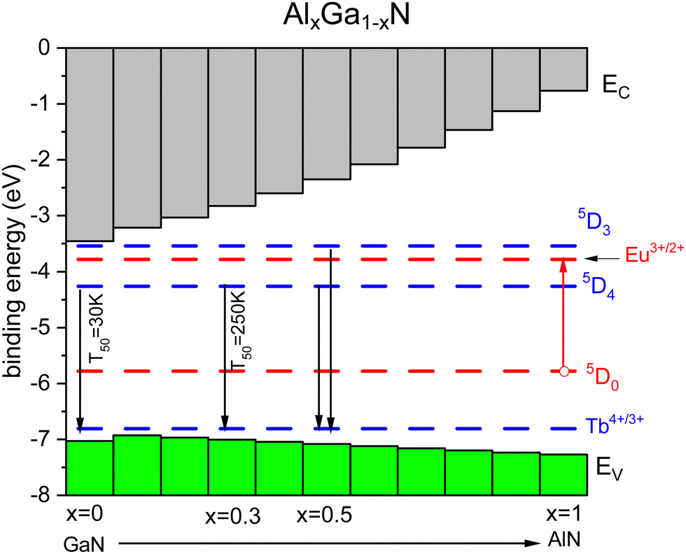 | ||
| Fig. 9 Stacked VRBE scheme of the Al1−xGaxN system with the Tb3+ ground and excited state levels. The Eu3+ ground and excited 5D0 levels are drawn as hole states. | ||
Horiai et al.190 showed that upon replacing 20% of the Y3+ in YAlO3 for Lu3+, the T50 for Ce3+ increases from 683 K to 767 K. With a slope relationship of 850 K eV−1, 0.1 eV increase of the CB-bottom can already accomplish this increase. Lu3+ has a smaller ionic radius than Y3+; the lattice parameters decrease and the bandgap and CB-bottom increase upon introducing Lu. Incorporating larger lanthanides such as Gd3+ and La3+ would likewise reduce the quenching temperature. Indeed, the T50 of GdAlO3 is only 345 K and for LaAlO3 there is no Ce3+ emission because the 5d-level is located above the CB-bottom. This is all illustrated by the corresponding data points in Fig. 8.
The sensitivity of T50 on slight changes in the ΔE is also well demonstrated with Ce3+ doped Y3Ga5O12. Depending on the synthesis temperature, part of the octahedral Ga3+ sites can be occupied by the larger Y3+ cations. This is known as the anti-site occupancy which leads to slight lattice expansion and band gap narrowing. In Czochralski grown crystals the Ce3+ emission is absent at 10 K197 but for powders grown with a relatively low temperature solid state synthesis there will be less anti-site occupancy, smaller lattice parameter, and wider bandgap. As a results the Ce3+ emission is observed at RT.198
Fig. 3 shows that the VRBE in the lowest 5d-state of Pr3+ is about 0.5 eV below that for Ce3+ and similar will hold for other compounds. This implies that when quenching proceeds via the CB, the T50 for the 4f15d–4f2 emission of Pr3+ should be about 400 K higher than that for Ce3+. For BaF2 indeed, the 5d–4f emission from Pr3+ is at least 200 K more stable than from Ce3+.146 However, the T50 values of Ce3+ and Pr3+ in Y3Al5−xGaxO12 are 640 K and 321 K for x = 0, 583 K and 377 K for x = 1, 491 K and 407 K for x = 2, 344 K and 316 K for x = 3, and 301 K and 173 K for x = 4.196,215 For x = 0, 1, 2, 3, and 4, T50 (Ce) decreases because the 5d VRBE moves up and the CB-bottom moves down. However, T50 (Pr) increases for x = 0, 1, and 2 and this was attributed to quenching via the crossing point (CP) of the 4f2 [3P2] and 4f5d parabola's where the former remains stationary and the latter moves up with increasing x.215 For x = 3 and 4, the CB moves down below the CP and both Ce and Pr quench via the CB. The question remains though why T50 (Pr) < T50 (Ce) for x = 3 and x = 4. T50 (Pr) < T50 (Ce) was also observed in Y2SiO5 and Lu2SiO5 by van der Kolk et al.216 where photocurrent studies did evidence quenching via the CB. It was suggested that the 1S0 4f2 level of Pr3+ located above the lowest energy 4f1 5d-level assists in the quenching via the CB thus lowering T50.216 The final answer remains open and deserves a more dedicated study.
IV. Summary and conclusions
This work confirmed that the thermal quenching of Eu3+, Tb3+, Pr3+, Eu2+, and Ce3+ emissions proceeds via charge transfer to the host band states. By using a frequency factor of 2 × 10¹³ Hz and the typical value for the radiative lifetime of the emitting energy level, the rate of change in T50 with a quenching energy barrier ΔE was predicted as shown in Table 1. Using the refined chemical shift model for the VRBE diagram construction, the ΔE values of thermal quenching were derived. For the characteristic 4fn–4fn emissions of Eu3+, Tb3+, and Pr3+, the predicted slopes T50/ΔE (K eV−1) were indeed observed. The 0.3–0.5 eV intercept with the horizontal in Fig. 4–6 was attributed partly to the relaxation energy accompanying the charge transfer and to the possibility/probability of quenching via the impurity trapped exciton state. The effect of relaxation is very compound dependent and is not accounted for in the VRBE diagram construction. When the quenching temperature is above 400 K for Pr3+, it was suggested that multi-phonon relaxation from 3P0 to 1D0 becomes a dominating route for quenching.The ΔE values for the 5d–4f emissions of Eu2+ and Ce3+ derived from VRBE diagrams carry substantial larger errors than those for Eu3+, Tb3+, and Pr3+. This is due to the contribution from the error in Eex, the Stokes ΔS and for Ce3 + also the U-value. These error sources are held responsible for the wide scatter of the the data points in Fig. 7 and 8. Nevertheless, clear trends are observed particularly when dealing with a sequence of a similar type of compounds like the garnet or rare earth perovskite family of compounds.
This work deals with about 170 different compounds, and for each of them all parameters needed to construct VRBE schemes like that for YPO4 in Fig. 3 have been provided in various tables. This work has demonstrated that changes as small as 0.1 eV in level locations may already lead to a 50–100 K shift in T50. Such changes can be accomplished by intentional or unintentional defects, the activator concentration, the occupation of anti-sites in garnets, and the application of pressure, synthesis conditions, etc. As a result, the often made assumption that ΔE in the Arrhenius equations is a constant will not hold for charge transfer quenching and then there is not much scientific sense in fitting a quenching curve with this Arrhenius equation. This work has also demonstrated the limitations of VRBE diagrams as shown in Fig. 3. (1) They do not deal with lattice relaxation effects leading to the very compound dependent Stokes shifts. (2) The assumption that the maximum of the Eu3+ charge transfer band always defines the energy difference between the Eu3+/2+ CTL and the VB-top may not hold for all types of compounds. One may not exclude a few 0.1 eV differences between fluorides, oxides, and sulfides leading to systematic errors in level locations and ΔE. (3) For compounds with different sites for the activator, the same U-value is always used. A few 0.1 eV differences between different sites cannot be excluded, and there are indications of such differences. (4) The used U-values are not rigorously based on experimental or theoretical evidence and may still carry substantial errors. Despite all the above limitations, consistency between the quenching data and VRBE diagrams has been demonstrated. With a more dedicated study one might then use the quenching data as a means to further improve the method of the VRBE-diagram construction and therewith its accuracy and predictive potential.
Conflicts of interest
There are no conflicts to declare.References
- H. Yamamoto, Proc. SPIE, 2010, 7598, 759808 CrossRef.
- P. Dai, X. Zhang, M. Zhou, X. Li, J. Yang, P. Sun, C. Xu and Y. Liu, J. Am. Ceram. Soc., 2012, 95, 658 CrossRef CAS.
- N. Rakov, S. A. Vieira, Q. P. S. Silva and G. S. Maciel, Sens. Actuators, B, 2015, 209, 407 CrossRef CAS.
- V. Lojpur, S. Culubrk, M. Medic and M. Dramicanin, J. Lumin., 2016, 170, 467 CrossRef CAS.
- R. A. Hansel, S. K. Desai, S. W. Allison, A. L. Heyes and D. G. Walker, J. Appl. Phys., 2010, 107, 016101 CrossRef.
- M. M. Gentleman and D. R. Clarke, Surf. Coat. Technol., 2005, 200, 1264 CrossRef CAS.
- M. D. Chambers and D. R. Clarke, Annu. Rev. Mater. Res., 2009, 39, 325 CrossRef CAS.
- P. Dorenbos, Phys. Rev. B: Condens. Matter Mater. Phys., 2012, 85, 165107 CrossRef.
- P. Dorenbos, J. Lumin., 2019, 214, 116536 CrossRef CAS.
- P. Dorenbos, J. Lumin., 2020, 222, 117164 CrossRef CAS.
- L.-J. Lyu and D. S. Hamilton, J. Lumin., 1991, 48–49, 251 CrossRef CAS.
- G. Gao, A. Turshatov, I. A. Howard, D. Busko, R. Joseph, D. Hudry and B. S. Richards, Adv. Sustainable Syst., 2017, 1, 1600033 CrossRef.
- P. Dorenbos, Opt. Mater., 2017, 69, 8 CrossRef CAS.
- P. Dorenbos, J. Lumin., 2018, 197, 62 CrossRef CAS.
- P. Dorenbos, J. Lumin., 2005, 111, 89 CrossRef CAS.
- G. Blasse, J. Chem. Phys., 1966, 45, 2356 CrossRef CAS.
- C. W. Struck and W. H. Fonger, J. Lumin., 1970, 1–2, 456 CrossRef.
- P. Dorenbos, J. Alloys Compd., 2009, 488, 568 CrossRef CAS.
- W. H. Fonger and C. W. Struck, J. Chem. Phys., 1970, 52, 6364 CrossRef CAS.
- Y. Kitagawa, J. Ueda, K. Arai, H. Kageyama and S. Tanabe, J. Appl. Phys., 2021, 129, 183104 CrossRef CAS.
- S. W. Allison and G. T. Gillies, Rev. Sci. Instrum., 1997, 68, 2615 CrossRef CAS.
- A. R. Bugos, S. W. Allison and M. R. Cates, IEEE Proceeding Southeastcon, 1991, 1141 Search PubMed.
- G. Blasse and J. de Vries, J. Electrochem. Soc.: Sol. State Sci., 1967, 114, 875 CrossRef CAS.
- E. P. Riedel, J. Lumin., 1970, 1(2), 176 CrossRef.
- M. D. Chambers, P. A. Rousseve and D. R. Clarke, Surf. Coat. Technol., 2008, 203, 461 CrossRef CAS.
- G. Blasse, A. Bril and J. A. de Poorter, J. Chem. Phys., 1970, 53, 4450 CrossRef CAS.
- H. Zhu, M. Fang, Z. Huan, Y. Liu, K. Chen, X. Min, Y. Mao and M. Wang, J. Lumin., 2016, 172, 180 CrossRef CAS.
- B. Bondzior, D. Stefanska, T. H. Q. Vu, N. Miniajluk-Gawel and P. J. Deren, J. Alloys and Comp., 2021, 852, 157074 CrossRef CAS.
- S. J. Park, J. Y. Kim, J. H. Yim, N. Y. Kim, C. H. Lee, S. J. Yang and H. K. Yang, J. Alloys and Comp., 2018, 741, 246 CrossRef CAS.
- R. J. L. Steenbakker, R. G. Wellman, J. R. Nicholls and J. P. Feist, Proc. of ASME Turbo Expo 2008: Power for Land Sea and Air GT2008, June 9–13, 2008, Berlin, Germany, GT2008-51192.
- K. S. Desai, R. A. Hansel, R. W. Pitz and D. G. Walker, 48th AIAA Aerospace Sciences Meeting Including the New Horizons Forum and Aerospace Exposition, 4–7 January 2010, Orlando, Florida, AIAA 2010-672.
- I. N. Ogorodnikov and V. A. Pustavarov, J. Lumin., 2015, 162, 50 CrossRef CAS.
- G. A. West and N. S. Clements, J. Lumin., 1992, 54, 245 CrossRef CAS.
- S. D. Alaruri, A. J. Brewington, M. A. Thomas and J. A. Miller, IEEE Trans. Instrum. and Meas., 1993, 42, 735 CrossRef CAS.
- J. Bang, B. Abrams and P. H. Holloway, J. Appl. Phys., 2003, 94, 7091 CrossRef CAS.
- V. Jary, L. Havlak, J. Barta, M. Buryi, E. M. M. Rejman, V. Laguta and M. Nikl, Materials, 2015, 8, 6978 CrossRef CAS PubMed.
- Y. Kitagawa, J. Ueda, M. G. Brik and S. Tanabe, Opt. Mater., 2018, 83, 111 CrossRef CAS.
- A. Wakahara, Opt. Mater., 2006, 28, 731 CrossRef CAS.
- T. Andreev, N. Quang Liem, Y. Hori, M. Tanaka, O. Oda, D. Le Si Dang and B. Daudin, Phys. Rev. B: Condens. Matter Mater. Phys., 2006, 73, 195203 CrossRef.
- C.-W. Lee, H. O. Everitt, D. S. Lee, A. J. Steckl and J. M. Zavada, J. Appl. Phys., 2004, 95, 7717 CrossRef CAS.
- P. Dorenbos, J. Phys.: Condens. Matter, 2003, 15, 8417 CrossRef CAS.
- P. Dorenbos and E. G. Rogers, ECS J. Solid State Sci. Technol., 2014, 3, R150 CrossRef CAS.
- P. Boutinaud, R. Mahiou, E. Cavalli and M. Bettinelli, Chem. Phys. Lett., 2006, 418, 185 CrossRef CAS.
- P. Boutinaud, P. Putaj, R. Mahiou, E. Cavalli and A. Speghini, Spectrosc. Lett., 2007, 40, 209 CrossRef CAS.
- D. F. Grabtree, J. Phys. D: Appl. Phys., 1975, 8, 2097 CrossRef.
- Z. Liang, J. Zhang, J. Sun, X. Li, L. Cheng, H. Zhong, S. Fu, Y. Tian and B. Chen, Phys. B, 2013, 412, 36 CrossRef CAS.
- Y. Tokida and S. Adachi, ECS J. Solid State Sci. Technol., 2014, 3, R100 CrossRef CAS.
- E. Cavalli, P. Boutinaud, R. Mahiou, M. Bettinelli and P. Dorenbos, Inorg. Chem., 2010, 49, 4916 CrossRef CAS PubMed.
- E. Cavalli, P. Boutinaud, T. Cucchietti and M. Bettinelli, Opt. Mater., 2009, 31, 470 CrossRef CAS.
- S. Schwung, D. Rytz, B. Heying, U. C. Rodewald, O. Niehaus, D. Enseling, T. Justel and R. Pottgen, J. Lumin., 2015, 166, 289 CrossRef CAS.
- P. Boutinaud, M. Bettinelli and F. Diaz, Opt. Mater., 2010, 32, 1659 CrossRef CAS.
- A. H. Krumpel, E. van der Kolk, P. Dorenbos, P. Boutinaud, E. Cavalli and M. Bettinelli, Mater. Sci. Eng., B, 2008, 146, 114 CrossRef CAS.
- A. H. Krumpel, E. van der Kolk, E. Cavalli, P. Boutinaud, M. Bettinelli and P. Dorenbos, J. Phys.: Condens. Matter, 2009, 21, 115503 CrossRef PubMed.
- W. Ryba-Romanowski, S. Golab, W. A. G. Dominiak-Dzik, M. N. Palatnikov and N. V. Sidorov, Appl. Phys. Lett., 2001, 78, 3610 CrossRef CAS.
- R. Lisiecki, B. Macalik, R. Kowalski, J. Komar and W. Ryba-Romanowski, Crystals, 2020, 10, 1034 CrossRef CAS.
- P. Boutinaud, E. Cavalli and M. Bettinelli, J. Phys.: Condens. Matter, 2007, 19, 386230 CrossRef.
- G. Blasse and A. Bril, J. Lumin., 1970, 3, 109 CrossRef CAS.
- E. Zych and D. Kulesza, Z. Naturforsch., 2014, 69b, 165 CrossRef.
- A. Wakahara, Y. Nakanishi, T. Fujiwara, A. Yoshida, T. Ohshima and T. Kamiya, Phys. Status Solidi A, 2005, 202, 863 CrossRef CAS.
- Y. Nakanishi, A. Wakahara, H. Okada, A. Yoshida, T. Ohshima and H. Itoh, Phys. Status Solidi B, 2003, 240, 372 CrossRef CAS.
- J. Rodrigues, M. Fialho, S. Magalhaes, M. R. Correia, L. Rino, E. Alves, A. J. Neves, K. Lorenz and T. Monteiro, J. Lumin., 2016, 178, 249 CrossRef CAS.
- P. Dorenbos, Opt. Mater., 2019, 91, 333 CrossRef CAS.
- E. Cavalli, A. Belletti, R. Mahiou and P. Boutinaud, J. Lumin., 2010, 130, 733 CrossRef CAS.
- Q. Wang, M. Xie, M. Fang, X. Wu, Y. Liu, Z. Huang, K. Xi and X. Min, Molecules, 2019, 24, 1295 CrossRef PubMed.
- A. Stanulis, A. Katelnikovas, M. VanBael, A. Hardy, A. Kareiva and T. Justel, J. Lumin., 2016, 172, 323 CrossRef CAS.
- L. Li, P. Yang, W. Xia, Y. Wang, F. Ling, Z. Cao, S. Jiang, G. Xiang, X. Zhou and Y. Wang, Ceram. Int., 2021, 47, 769 CrossRef CAS.
- E. Cavalli, F. Angiuli, P. Boutinaud and R. Mahiou, J. Solid State Chem., 2012, 185, 136 CrossRef CAS.
- C. Liu, F. Pan, Q. Peng, W. Zhou, R. Shi, L. Zhou, J. Zhang, J. Chen and H. Liang, J. Phys. Chem. C, 2016, 120, 26044 CrossRef CAS.
- P. Boutinaud, L. Sarakha, R. Mahiou, E. Cavalli, M. Bettinelli, P. Dorenbos and R. Mahiou, J. Phys. D: Appl. Phys., 2009, 42, 045106 CrossRef.
- S. Okamoto, H. Kobayashi and H. Yamamoto, J. Appl. Phys., 1999, 86, 5594 CrossRef CAS.
- Y. Wang, V. Tsiumra, Q. Peng, H. Liang, Y. Zhydachevskyy, M. Chaika, P. Dluzewski, H. Przybylinska and A. Suchocki, J. Phys. Chem. A, 2019, 123, 4021 CrossRef CAS PubMed.
- R. Shi, L. Lin, P. Dorenbos and H. Liang, J. Mater. Chem. C, 2017, 5, 10737 RSC.
- X. Zhang, Q. Zhu, B. Chen, S. Wang, A. L. Rogach and F. Wang, Adv. Photonics Research, 2021, 2, 2000089 CrossRef.
- G. Blasse and A. Meijerink, Inorg. Chim. Acta, 1989, 160, 29 CrossRef CAS.
- H. J. Lozykowski, W. M. Jadwisienczak and I. Brown, J. Appl. Phys., 2000, 88, 210 CrossRef CAS.
- Y. E. Romanyuk, L. D. Kranz and S. R. Leone, J. Appl. Phys., 2008, 103, 073104 CrossRef.
- P. Dorenbos, J. Phys.: Condens. Matter, 2005, 17, 8103 CrossRef CAS.
- Y. Jia, A. Miglio, S. Ponce, M. Mikami and X. Gonze, Phys. Rev. B: Condens. Matter Mater. Phys., 2017, 96, 125132 CrossRef.
- P. Dorenbos, IEEE Trans. Nucl. Sci., 2010, 57, 1162 CAS.
- P. Dorenbos, J. Lumin., 2003, 104, 239 CrossRef CAS.
- V. Bachmann, C. Ronda, O. Oeckler, W. Schnick and A. Meijerink, Chem. Mater., 2009, 21, 316 CrossRef CAS.
- W. Drozdowski and A. J. Wojtowicz, Nucl. Instrum. Methods Phys. Res., Sect. A, 2002, 486, 412 CrossRef CAS.
- G. Munoz, C. de la Cruz, A. Munoz and O. J. Rubio, J. Mater. Sci. Lett., 1988, 7, 1310 CrossRef CAS.
- V. Yakovlev, L. Trefilova, A. Meleshko and N. Ovcharenko, J. Lumin., 2012, 132, 2476 CrossRef CAS.
- F. Jaque, J. A. Hernandez, H. S. Murrieta and J. O. Rubio, J. Phys. Soc. Jpn., 1982, 51, 249 CrossRef CAS.
- P. Wang, J. Mao, X. Wei, L. Qiu, B. Jiang, F. Chi, M. Yina and Y. Chen, J. Alloys and Comp., 2021, 869, 159277 CrossRef CAS.
- Y. Wei, X. Qi, H. Xiao, W. Luo, H. Yao, L. Lv, G. Li and J. Lin, RSC. Adv., 2016, 6, 43771 RSC.
- A. Garcia, B. Latourrette and C. Fouassier, J. Electrochem. Soc.: Sol. State Science and Techn., 1979, 126, 1734 CrossRef CAS.
- J. Zheng, S. Wu, G. Chen, S. Dang, Y. Zhuang, Z. Guo, Y. Lu, Q. Cheng and C. Chen, J. Alloys and Comp., 2016, 663, 332 CrossRef CAS.
- Z. Xia, L. Liao, Z. Zhang and Y. Wang, Mater. Res. Bull., 2012, 47, 405 CrossRef CAS.
- J. Wang, M. Zhang, Q. Zhang, W. Ding and Q. Su, Appl. Phys. B, 2007, 87, 249 CrossRef CAS.
- W. L. Wanmaker and J. W. ter Vrugt, Phil. Res. Rept., 1967, 22, 355 CAS.
- G. B. Nair, H. C. Swart and S. J. Dhoble, J. Lumin., 2019, 214, 116564 CrossRef CAS.
- W.-R. Liu, Y.-C. Chiu, Y.-T. Yeh, S.-M. Jang and T.-M. Chen, J. Electrochem. Soc., 2009, 156, J169 Search PubMed.
- C. Qin, Y. Huang, L. Shi, G. Chen, X. Qiao and H. J. Seo, J. Phys. D: Appl. Phys., 2009, 42, 185105 CrossRef.
- C. Zhao, Z. Xia and M. Li, RSC Adv., 2014, 4, 33114 RSC.
- J. Zeler, M. Sulollari, A. Meijerink, M. Bettinelli and E. Zych, J. Alloys Compd., 2020, 844, 156096 CrossRef CAS.
- G. Blasse, A. Bril and J. de Vries, J. Electrochem. Soc.:Sol. State Sci., 1968, 115, 977 CrossRef CAS.
- Y. Xie, S. Zhang, Q. Zeng, Z. Pei and Q. Su, J. Mater. Sci. Technol., 2004, 20, 517 CAS.
- M. Leskela, T. Koskentalo and G. Blasse, J. Sol. St. Chem., 1985, 59, 272 CrossRef CAS.
- A. Diaz and D. A. Keszler, Chem. Mater., 1997, 9, 2071 CrossRef CAS.
- J. Huang, J. Dai, D. Deng, H. Yu, Y. Li, Y. Hua, S. Zhao, C. Li and S. Xu, RSC Adv., 2015, 5, 85682 RSC.
- G. Blasse, A. Bril and J. de Vries, J. Inorg. Nucl. Chem., 1969, 31, 568 CrossRef CAS.
- S. J. Camardello, P. J. Toscano, M. G. Brik and A. M. Srivastava, Opt. Mater., 2014, 37, 404 CrossRef CAS.
- S. H. M. Poort, H. M. Reijnhoudt, H. O. T. van der Kuip and G. Blasse, J. Alloys Compd., 1996, 241, 75 CrossRef CAS.
- F. Su, B. Lou, Y. Ou, Y. Yang, W. Zhou, C.-K. Duan and H. Liang, J. Phys. Chem. C125, 2021, 595 Search PubMed.
- G. Blasse, W. L. Wanmaker, J. W. ter Vrugt and A. Bril, Philips Res. Rep., 1968, 23, 189 CAS.
- J. Yan, C. Liu, J. Vlieland, J. Zhou, P. Dorenbos, Y. Huang, Y. Tao and H. Liang, J. Lumin., 2017, 183, 97 CrossRef CAS.
- A. A. Setlur, A. M. Srivastava, L. Pham, M. Hannah and U. Happek, J. Appl. Phys., 2008, 103, 053513 CrossRef.
- D. Jia, W. Jia and Y. Jia, J. Appl. Phys., 2007, 101, 023520 CrossRef.
- D. Hou, C. Liu, X. Ding, X. Kuang, H. Liang, S. Sun, Y. Huang and Y. Tao, J. Mater. Chem. C, 2013, 1, 493 RSC.
- D. Hou, W. Chen, X. Ding, H. Liang, L. Zheng and J. Zhang, ECS J. Solid State Sci. Technol., 2013, 2, R79 CrossRef CAS.
- K. Asami, J. Ueda, K. Yasuda, K. Hongo, R. Maezono, M. G. Brik and S. Tanabe, Opt. Mater., 2018, 84, 436 CrossRef CAS.
- L. Lin, L. Ning, R. Zhou, C. Jiang, M. Peng, Y. Huang, J. Chen, Y. Huang, Y. Tao and H. Liang, Inorg. Chem., 2018, 57, 7090 CrossRef CAS PubMed.
- M. Yamaga, Y. Masui, S. Sakuta, N. Kodama and K. Kaminaga, Phys. Rev. B: Condens. Matter Mater. Phys., 2005, 71, 205102 CrossRef.
- G. Blasse and A. Bril, J. Chem. Phys., 1968, 48, 217 CrossRef CAS.
- T. L. Barry, ECS J. Solid State Sci. Technol., 1968, 115, 1181 CAS.
- S. S. B. Nasir, A. Tanaka, S. Yoshiara and A. Kato, J. Lumin., 2019, 207, 22 CrossRef CAS.
- T. J. Isaacs, ECS J. Solid State Sci. Technol., 1971, 118, 1009 CAS.
- D. Stefanska and P. J. Deren, Opt. Mater., 2018, 80, 62 CrossRef CAS.
- J. Zhong, W. Zhao, L. Lan and J. Wang, J. Mater. Sci.: Mater. Electron., 2014, 25, 736 CrossRef CAS.
- Q. Shao, H. Lin, Y. Dong, Y. Fu, C. Liang, J. He and J. Jiang, J. Solid State Chem., 2015, 225, 72 CrossRef CAS.
- H. Aizawa, S. Komuro, T. Katsumata, S. Sato and T. Morikawa, Thin Solid Films, 2006, 496, 179 CrossRef CAS.
- S. H. M. Poort, W. P. Blokpoel and G. Blasse, Chem. Mater., 1995, 7, 1547 CrossRef CAS.
- F.-C. Lu, L.-J. Bai, W. Dang, Z.-P. Yang and P. Lin, ECS J. Solid State Sci. Technol., 2015, 4, R27 CrossRef CAS.
- D. Dutczak, T. Justel, C. Ronda and A. Meijerink, Phys. Chem. Chem. Phys., 2015, 17, 15236 RSC.
- J. Botterman, J. J. Joos and P. F. Smet, Phys. Rev. B: Condens. Matter Mater. Phys., 2014, 90, 085147 CrossRef CAS.
- J. Bierwagen, S. Yoon, N. Gartmann, B. Walfort and H. Hagemann, Opt. Mater. Express, 2016, 6, 793 CrossRef CAS.
- D. Dutczak, C. Ronda, T. Justel and A. Meijerink, J. Phys. Chem. A, 2014, 118, 1617 CrossRef CAS PubMed.
- Y. Luo and Z. Xia, Opt. Mater., 2014, 36, 1874 CrossRef CAS.
- T. Hu, Y. Gao, M. Molokeev, Z. Xia and Q. Zhang, Sci. China. Mater., 2019, 62, 1807 CrossRef CAS.
- G. Blasse and A. Bril, Philips Res. Rep., 1968, 23, 201 CAS.
- C. E. Tyner and H. G. Drickamer, J. Chem. Phys., 1977, 67, 4116 CrossRef CAS.
- S. H. M. Poort, A. Meyerink and G. Blasse, J. Phys. Chem. Sol., 1997, 58, 1451 CrossRef CAS.
- P. F. Smet, N. Avci and D. Poelman, J. Electrochem Soc., 2009, 156, H243 CrossRef CAS.
- C. Chartier, C. Barthou, P. Benalloul and J. M. Frigerio, J. Lumin., 2005, 111, 147 CrossRef CAS.
- J. J. Joos, K. W. Meert, A. B. Parmentier, D. Poelman and P. F. Smet, Opt. Mater., 2012, 34, 1902 CrossRef CAS.
- P. Benalloul, C. Barthou, C. Fouassier, A. N. Georgobiani, L. S. Lepnev, Y. N. Emirov, A. N. Grutzintsev, B. G. Tagiev, O. B. Tagiev and R. B. Jabbarov, J. Electrochem. Soc., 2003, 150, G62 CrossRef CAS.
- M. Ando and Y. A. Ono, J. Cryst. Growth, 1992, 117, 969 CrossRef CAS.
- V. Bachmann, A. Meijerink and C. Ronda, J. Lumin., 2009, 129, 1341 CrossRef CAS.
- R.-J. Xie, N. Hirosaki, N. Kimura, K. Sakuma and M. Mitomo, Appl. Phys. Lett., 2007, 90, 191101 CrossRef.
- J. Li, B. Lei, J. Qin, Y. Liu and X. Liu, J. Am. Ceram. Soc., 2013, 96, 873 CrossRef CAS.
- J. Ueda, S. Tanabe, K. Takahashi, T. Takeda and N. Hirosaki, Bull. Chem. Soc. Jpn., 2018, 91, 173 CrossRef CAS.
- J. Tian, W. Zhuang, R. Liu, L. Wang, Y. Liu, C. Yan, G. Chen, H. Xu, M. Chen, Z. Jiang and X. Zhang, J. Am. Ceram. Soc., 2019, 102, 7336 CrossRef CAS.
- P. Pust, C. Hecht, V. Weiler, A. Locher, D. Zitnanska, S. Harm, D. Weichert, P. J. Schmidt and W. Schnick, Chem. Mater., 2014, 26, 6113 CrossRef CAS.
- R. Shendrik and E. Radzhabov, IEEE Trans. Nucl. Sci., 2010, 57, 1295 CAS.
- P. Dorenbos, R. Visser, C. W. E. van Eijk, R. W. Hollander and H. W. den Hartog, Nucl. Instrum. Methods, 1991, A310, 236 CrossRef CAS.
- R. C. Tailor, O. H. Nestor and B. Utts, IEEE TNS-33, 1986, 243 CAS.
- G. Bizarri, J. T. M. de Haas, P. Dorenbos and C. W. E. van Eijk, Phys. Status Solidi A, 2006, 203, R41 CrossRef CAS.
- A. M. Srivastava, S. J. Camardello, H. A. Comanzo, M. Aycibin and U. Happek, Opt. Mater., 2010, 32, 936 CrossRef CAS.
- X. Zhang, B. Park, N. Choi, J. Kim, G. C. Kim and J. H. Yoo, Mater. Lett., 2009, 63, 700 CrossRef CAS.
- Z. Fu-Tan, C. Li-Yun and X. Xu-Rong, ECS J. Solid State Sci. Technol., 1987, 134, 3186 Search PubMed.
- D. M. de Leeuw, C. A. H. A. Mutsaers, H. Mulder and D. B. M. Klaasen, ECS J. Solid State Sci. Technol., 1988, 135, 1009 CAS.
- P. Dorenbos, unpublished data.
- T. Shalapska, G. Stryganyuka, D. Trotsc, T. Demkiv, A. Gektin, A. Voloshinovskii and P. Dorenbos, J. Lumin., 2010, 130, 1941 CrossRef CAS.
- T. Justel, P. Huppertz, W. Mayr and D. U. Wiechert, J. Lumin., 2004, 106, 225 CrossRef CAS.
- C.-H. Huang, T.-M. Chen and B.-M. Cheng, Inorg. Chem., 2011, 50, 6552 CrossRef CAS PubMed.
- H. Lin, H. Liang, Z. Tian, B. Han, J. Wang and Q. Su, J. Phys. D: Appl. Phys., 2009, 42, 165409 CrossRef.
- Y. Yang, B. Lou, Y. Ou, F. Su, C.-G. Ma, C.-K. Duan, P. Dorenbos and H. Liang, Inorg. Chem., 2022, 61, 7654 CrossRef CAS PubMed.
- J. F. Chen, Y. Li, G.-L. Song, D.-M. Yao, L.-Y. Yuan, X.-J. Qi and S.-H. Wang, J. Inorg. Mater., 2007, 22(1), 25 CAS.
- I. N. Ogorodnikov, N. E. Poryvai, I. N. Sedunova, A. V. Tolmachev and R. P. Yavetskiy, Opt. Spectrosc., 2011, 110, 266 CrossRef CAS.
- Y. Ou, W. Zhou, D. Hou, M. G. Brik, P. Dorenbos, Y. Huang and H. Liang, RSC Adv., 2019, 9, 7908 RSC.
- Q. Wei, G. Liu, Z. Zhou, J. Wan, H. Yang and Q. Liu, Mater. Lett., 2014, 126, 178 CrossRef CAS.
- V. Jary, L. Havlak, J. Barta, E. Mihokova and M. Nikl, IEEE Trans. Nucl. Sci., 2014, 61, 385 CAS.
- O. Sidletskiy, V. Baumer, I. Gerasymov, B. Grinyov, K. Katrunov, N. Starzhinsky, O. Tarasenko, V. Tarasov, S. Tkachenko, O. Voloshina and O. Zelenskaya, Rad. Meas., 2010, 45, 365 CrossRef CAS.
- V. Jary, M. Nikl, S. Kurosawa, Y. Shoji, E. Mihokova, A. Beitlerova, G. P. Pazzi and A. Yoshikawa, J. Phys. Chem. C, 2014, 118, 26529 CrossRef.
- L. Pidol, A. Kahn-Harari, B. Viana, B. Ferrand, P. Dorenbos, C. W. E. van Eijk and E. Virey, J. Phys.: Cond. Matter., 2003, 15, 2091 CrossRef CAS.
- H. Feng, D. Ding, H. Li, S. Lu, S. Pan, X. Chen and G. Ren, J. Alloys Comp., 2011, 509, 3855 CrossRef CAS.
- A. Pfahnl, Bell Syst. Tech., 1963, 181 CrossRef CAS.
- R. Shi, J. Xu, G. Liu, X. Zhang, W. Zhou, F. Pan, Y. Huang, Y. Tao and H. Liang, J. Phys. Chem. C, 2016, 120, 4529 CrossRef CAS.
- J. M. Herzog, D. Witkowski and D. A. Rothamer, Meas. Sci. Technol., 2021, 32, 054008 CrossRef CAS.
- S. K. Sharma, Y.-C. Lin, I. Carrasco, T. Tingberg, M. Bettinelli and M. Karlsson, J. Mater. Chem. C, 2018, 6, 8923 RSC.
- L. Zhou, W. Zhou, R. Shi, C. Liu, Y. Huang, Y. Tao and H. Liang, J. Lumin., 2016, 177, 178 CrossRef CAS.
- Z. Xia, M. S. Molokeev, W. B. Im, S. Unithrattil and Q. Liu, J. Phys. Chem. C, 2015, 119, 9488 CrossRef CAS.
- H. Suzuki, T. A. Tombrello, C. L. Melcher and J. S. Schweitzer, IEEE Trans. Nucl. Sci., 1994, 41, 681 CAS.
- K. Mori, M. Nakayama and H. Nishimura, Phys. Rev. B: Condens. Matter Mater. Phys., 2003, 67, 165206 CrossRef.
- E. Mihokova, K. Vavru, M. P. Horodysky, W. Chewpraditkul, V. Jary and M. Nikl, IEEE Trans. on Nucl. Sci., 2012, 59, 2085 CAS.
- V. Jary, M. Nikl, E. Mihokova, J. A. Mares, P. Prusa, P. Horodysky, W. Chewpraditkul and A. Beitlerova, IEEE Trans. Nucl. Sci., 2012, 59, 2079 CAS.
- J. D. Peak, C. J. Melcher and P. D. Rack, J. Applied Phys., 2011, 110, 013511 CrossRef.
- H. Luo, L. Ning, Y. Dong, A. J. J. Bos and P. Dorenbos, J. Phys. Chem. C, 2016, 120, 28743 CrossRef CAS.
- T. Shimizu, J. Ueda and S. Tanabe, Phys. Stat. Sol. C, 2012, 12, 2296 Search PubMed.
- L. Lin, R. Shi, R. Zhou, Q. Peng, C. Liu, Y. Tao, Y. Huang, P. Dorenbos and H. Liang, Inorg. Chem., 2017, 56, 12476 CrossRef CAS PubMed.
- J. M. Ogieglo, A. Katelnikovas, A. Zych, T. Justel, A. Meijerink and C. R. Ronda, J. Phys. Chem. A, 2013, 117, 2479 CrossRef CAS PubMed.
- I. V. Berezovskaya, A. S. Voloshinovskii, Z. A. Khapko, O. V. Khomenko, N. P. Efryushina and V. P. Dotsenko, Funct. Mater., 2021, 28, 6 CAS.
- E. van der Kolk, P. Dorenbos, J. T. M. de Haas and C. W. E. van Eijk, Phys. Rev. B: Condens. Matter Mater. Phys. 71, 2005, 045121 CrossRef.
- Y. Wang, R. Hrubiak, S. Turczynski, D. A. Pawlak, M. Malinowski, D. Wlodarczyk, K. M. Kosyl, W. Paszkowicz, H. Przybylinska, A. Wittlin, A. Kaminska, Y. Zhydachevskyy, M. G. Brik, L. Li, C.-G. Ma and A. Suchocki, Acta Mater., 2019, 165, 346 CrossRef CAS.
- M. J. Weber, Solid State Commun., 1973, 12, 741 CrossRef CAS.
- J. Ueda, P. Dorenbos, A. J. J. Bos, A. Meijerink and S. Tanabe, J. Phys. Chem. C, 2015, 119, 25003 CrossRef CAS.
- J. Ueda, K. Aishima and S. Tanabe, Opt. Mater., 2013, 35, 1952 CrossRef CAS.
- T. Horiai, J. Pejchal, J. Paterek, R. Kucerkova, Y. Yokota, A. Yoshikawa and M. Nikl, Jpn. J. Appl. Phys., 2022, 61, 072002 CrossRef.
- M. Jiao, W. Lv, L. Wei, Q. Zhao, B. Shao and H. You, Chem. Phys. Chem., 2015, 16, 817 CrossRef CAS PubMed.
- I. Venevtsev, V. Khanin, P. Rodnyi, H. Wieczorek and C. Ronda, IEEE Trans. Nucl. Sci., 2018, 65, 2090 CAS.
- J. M. Ogieglo, Luminescence and energy transfer in garnet scintillators, Thesis, University of Utrecht, 2012 Search PubMed.
- K. Kamada, T. Endo, K. Tsutumi, T. Yanagida, Y. Fujimoto, A. Fukabori, A. Yoshikawa, J. Pejchal and M. Nikl, Cryst. Growth Des., 2011, 11, 4484 CrossRef CAS.
- T. Lesniewski, S. Mahlik, K. Asami, J. Ueda, M. Grinberg and S. Tanabe, Phys. Chem. Chem. Phys., 2018, 20, 18380 RSC.
- J. Ueda, P. Dorenbos, A. J. J. Bos, K. Kuroishi and S. Tanabe, J. Mater. Chem. C, 2015, 3, 5642 RSC.
- A. Wittlin, H. Przybylinska, M. Berkowski, A. Kaminska, P. Nowakowski, P. Sybilski, C.-G. Ma, M. G. Brik and A. Suchocki, Opt. Mater. Express, 2015, 5, 243542 Search PubMed.
- X. Liu, X. Wang and W. Shun, Phys. Status Solidi A, 1987, 101, K161 CrossRef CAS.
- V. Jary, E. Mihokova, M. Nikl, P. Bohacek, A. Lauria and A. Vedda, Opt. Mater., 2010, 33, 149 CrossRef CAS.
- A. A. Setlur and U. Happek, J. Solid State Chem., 2010, 183, 1127 CrossRef CAS.
- Y. Chen, K. W. Cheah and M. Gong, J. Lumin., 2011, 131, 1770 CrossRef CAS.
- Q. Zhang, H. Ni, L. Wang and F. Xiao, ECS J. Solid State Sci. Technol., 2016, 5, R34 CrossRef CAS.
- H. Luo, A. J. J. Bos and P. Dorenbos, J. Phys. Chem. C, 2017, 121, 8760 CrossRef CAS PubMed.
- A. Bessiere, P. Dorenbos, C. W. E. van Eijk, E. Yamagishi, C. Hidaka and T. Takizawa, J. Electrochem. Soc., 2004, 151, H254 CrossRef CAS.
- B. Dierre, R.-J. Xie, N. Hirosaki and T. Sekiguchi, J. Mater. Res., 2007, 22, 1933 CrossRef CAS.
- L. Zhang, J. Zhang, X. Zhang, Z. Hao, H. Zhao and Y. Luo, ACS Appl. Mater. Interfaces, 2013, 5, 12839 CrossRef CAS PubMed.
- T. Suehiro, N. Hirosaki and R.-J. Xie, ACS Appl. Mater. Interfaces, 2011, 3, 811 CrossRef CAS PubMed.
- T. Suehiro, N. Hirosaki, R.-J. Xie and T. Sato, Appl. Phys. Lett., 2009, 95, 051903 CrossRef.
- J. Ueda and S. Tanabe, Opt. Mater.: X, 2019, 1, 100018 CAS.
- P. Dorenbos, J. Lumin., 2000, 91, 155 CrossRef CAS.
- P. Dorenbos, J. Lumin., 2013, 135, 93 CrossRef CAS.
- P. Dorenbos, J. Lumin., 2013, 136, 122 CrossRef CAS.
- P. Dorenbos and E. van der Kolk, Opt. Mater., 2008, 30, 1052 CrossRef CAS.
- K. Wang, K. P. O'Donnel, B. Hourahine, R. W. Martin, I. M. Watson, K. Lorenz and E. Alves, Phys. Rev. B: Condens. Matter Mater. Phys., 2009, 80, 125206 CrossRef.
- J. Ueda, A. Meijerink, P. Dorenbos, A. J. J. Bos and S. Tanabe, Phys. Rev. B, 2017, 95, 014303 CrossRef.
- E. van der Kolk, P. Dorenbos, C. W. E. van Eijk, S. A. Basun, G. F. Imbusch and W. M. Yen, Phys. Rev. B: Condens. Matter Mater. Phys., 2005, 71, 165120 CrossRef.
| This journal is © The Royal Society of Chemistry 2023 |