
P- and N-dopable ambipolar bulk heterojunction thermoelectrics based on ladder-type conjugated polymers†
Qiang
He‡
 ac,
Teck Lip Dexter
Tam‡
*b,
Xue Qi
Koh
c,
Nguk Neng
Tham
c,
Hong
Meng
*de,
Wei
Huang
*a and
Jianwei
Xu
*bcf
ac,
Teck Lip Dexter
Tam‡
*b,
Xue Qi
Koh
c,
Nguk Neng
Tham
c,
Hong
Meng
*de,
Wei
Huang
*a and
Jianwei
Xu
*bcf
aFrontiers Science Center for Flexible Electronics (FSCFE), Institute of Flexible Electronics (IFE), Northwestern Polytechnical University (NPU), 127 West Youyi Road, Xian 710072, P. R. China. E-mail: iamwhuang@nwpu.edu.cn
bInstitute of Sustainability for Chemical, Engineering and Environment (ISCE2), Agency of Science, Technology and Research (A*STAR), 1 Pesek Road, Singapore 627833, Singapore. E-mail: dexter-tam@isce2.a-star.edu.sg; jw-xu@imre.a-star.edu.sg
cInstitute of Materials Research and Engineering (IMRE), Agency of Science, Technology and Research (A*STAR), 2 Fusionopolis Way, Innovis, Singapore 138634, Singapore
dSchool of Electronics and Information, Northwestern Polytechnical University, 127 West Youyi Road, Xi'an, 710072, P. R. China. E-mail: menghong@nwpu.edu.cn
eSchool of Advanced Materials, Peking University Shenzhen Graduate School, 2199 Lishui Road, Shenzhen, 518055, P. R. China
fDepartment of Chemistry, National University of Singapore, 3 Science Drive 3, Singapore 117543, Singapore
First published on 25th November 2022
Abstract
Ambipolar bulk heterojunction polymer thermoelectrics were demonstrated for the first time using a classic n-type poly(benzimidazobenzophenanthrolinedione) ladder polymer (BBL) and a new p-type 6H-pyrrolo[3,2-b:4,5-b′]bis[1,4]benzothiazine ladder polymer (PBBTL). The blend films were solution-processed and can be p-/n-doped using a FeCl3/benzyl viologen radical cation (BV˙+). Well-balanced p- and n-doped conductivities can be achieved at a 1![[thin space (1/6-em)]](https://www.rsc.org/images/entities/char_2009.gif) :1 blend ratio, and a full thermoelectric device consisting of a pair of p- and n-channel legs from a single layer blend film was fabricated. The full device exhibited a power density of 0.27 μW cm−2 at ΔT = 3 K, operating at a voltage of 0.93 mV and a current density of 0.29 mA cm−2. The simplification of the device fabrication process using such ambipolar bulk heterojunction blend films may help the realization of polymer micro-thermoelectric devices in the future.
:1 blend ratio, and a full thermoelectric device consisting of a pair of p- and n-channel legs from a single layer blend film was fabricated. The full device exhibited a power density of 0.27 μW cm−2 at ΔT = 3 K, operating at a voltage of 0.93 mV and a current density of 0.29 mA cm−2. The simplification of the device fabrication process using such ambipolar bulk heterojunction blend films may help the realization of polymer micro-thermoelectric devices in the future.
Introduction
Semiconducting conjugated polymers have been gaining attention in organic light-emitting diodes (OLEDs), organic photovoltaics (OPVs), organic field-effect transistors (OFETs) and organic electrochromics (OECs) for the past two to three decades due to their intriguing electronic properties, as well as their potential to be solution processable, lightweight and mechanically robust.1–7 Their low cost and low toxicities make conjugated polymers excellent materials for wearable devices.8,9 In recent years, there has been substantial interest in using doped conjugated polymers for organic thermoelectric (OTE) application due to their relatively higher elemental abundance (C, N, S, and O) and low toxicity as compared to their inorganic counterparts.10–12 OTEs can be used as energy harvesters or temperature sensors in wearable devices by taking full advantage of conjugated polymer properties. Even more recently, OTEs have been demonstrated as cooling devices by making use of the Peltier effect.13In thermoelectric devices, the use of both p- and n-channel legs (instead of using metals to replace one of the elements) will result in more efficient device performance due to the larger differences in the thermal voltage (both p- and n-channel contributions) and larger thermal resistance (metals have much higher thermal conductivity). Micro-thermoelectric devices, with their smaller dimensions than their macroscopic counterparts, can provide a faster response, higher temperature resolution and greater power density.14 These properties, together with their inherent smaller size, make micro-thermoelectric devices very suitable for wearable devices. While both p- and n-channel legs of large devices can be screen-printed with ease, micro-thermoelectric devices with dimensions of a few tens of microns will face technical difficulties even with inkjet printing.15 The use of both p- and n-channel legs in micro-thermoelectric devices is even more crucial due to the need to maintain a thermal gradient over small distances. One way to overcome the need to separately print the micron-size p- and n-channel legs using p- and n-type polymers is to use an ambipolar polymer that can be either p- or n-doped to form the respective p- and n-channel legs in selected areas using fabrication techniques such as thermal evaporation of p- and n-dopants via shadow-masks. Such an approach allows the fabrication of small devices with dimensions down to 10 μm,16 without the need of micropatterning the p- and n-channel legs separately, while still taking advantage of the solution-processability of the polymer.
Easier said than done, there is only one very recent report on an ambipolar conjugated polymer doped using p- and n-dopants for OTEs, achieving maximum p- and n-doped conductivities of 1.6 and 2.75 × 10⁻⁵ S cm−1, respectively, and maximum power factors of ∼1 and ∼0.003 μW m−1 K−2 for p- and n-doping, respectively.20 The lack of ambipolar conjugated polymers that can be both p- and n-doped is due to the frontier molecular orbital energy levels, i.e., the ambipolar conjugated polymer must have the suitable highest occupied molecular orbital (HOMO) and lowest unoccupied molecular orbital (LUMO) energy levels that can be oxidized and reduced by the p- and n-dopants, respectively. Such a criterion will require the careful design of conjugated polymers, and the resulting polymers should also have balanced hole and electron transport properties. Alternatively, a blend of p- and n-type conjugated polymers may also accomplish the same result. Such a blend of p- and n-type conjugated polymers is analogous to the all-polymer bulk heterojunction (BHJ) OPVs that have shown a dramatic power efficiency improvement over the past decade,21 and more recently in high-performance BHJ OECTs.19 Interestingly, the use of p- and n-type conjugated polymer BHJ has not been demonstrated in OTEs, albeit the stimulating work on density of states engineering using pure p- or n-type blends reported by the groups of Katz, Campoy-Quiles and Kemerink.22–26 Here, we describe for the first time the use of p- and n-type ladder conjugated polymer (PBBTL as p-type and BBL as n-type) blends that can be either p- or n-doped for OTEs (Fig. 1). The thermoelectric properties of individual p-doped PBBTL and n-doped BBL have been investigated by us and other research groups previously.18,27–31 The thermoelectric performance of the BHJ film can be tuned not only by varying the doping time, but also by varying the p- and n-type polymer ratios. A full thermoelectric device based on a pair of p- and n-channel legs was fabricated using a 1:1 BHJ blend film doped at 1 s immersion for both p- and n-doping, respectively, demonstrating the simplicity of such a device architecture. Under such conditions, power factors of 2.18 ± 0.17 and 1.12 ± 0.19 μW m−1 K−2 for p- and n-doped BHJ films can be achieved, respectively, and the full device exhibited a power density of 0.27 μW cm−2 at ΔT = 3 K, operating at a voltage of 0.93 mV and a current density of 0.29 mA cm−2. While the devices fabricated here are not in the micron dimension, we foresee that the simplified processing arising from using a single ambipolar blend film will enable the realization of polymer micro-thermoelectrics in the future.
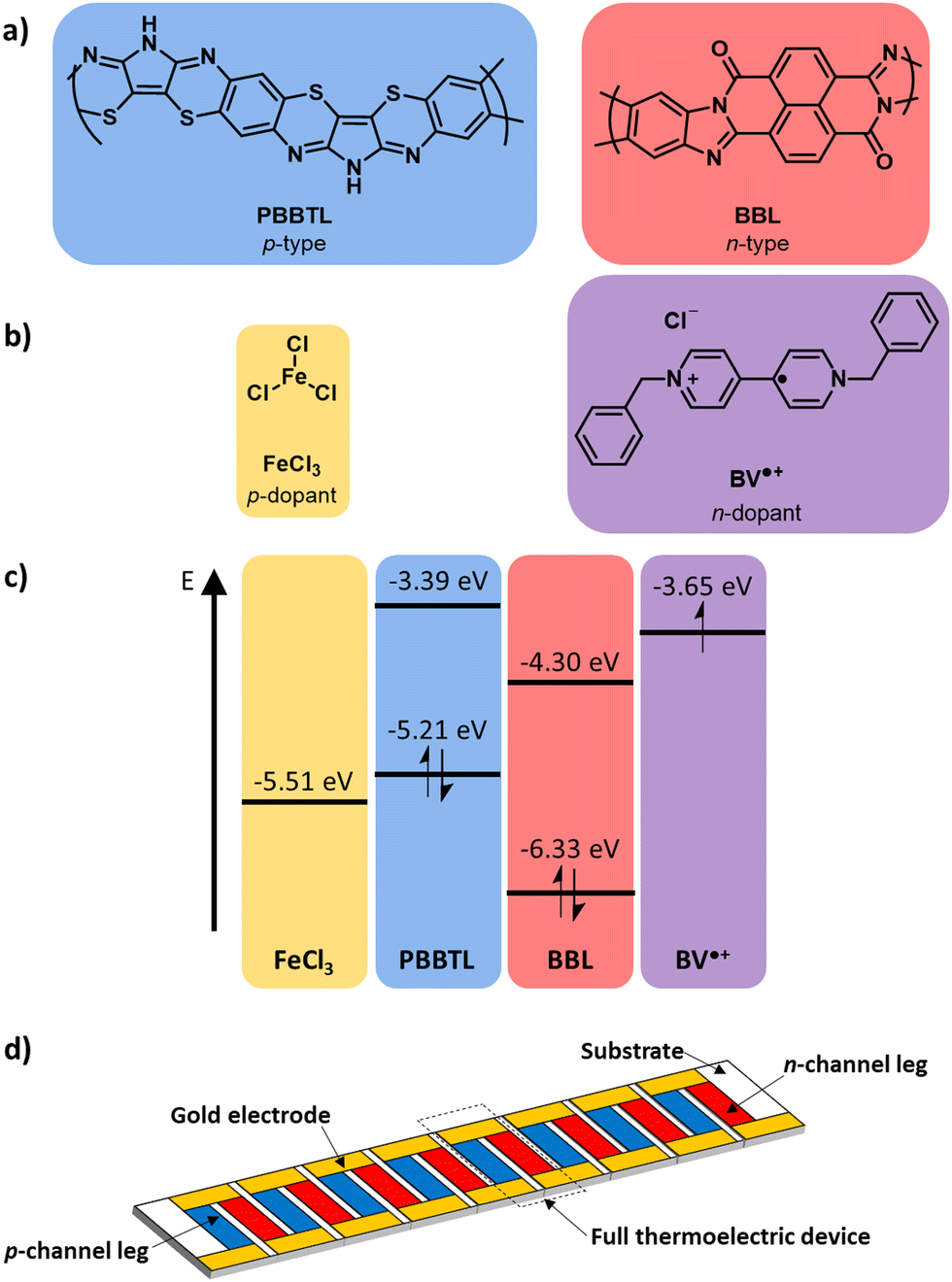 | ||
| Fig. 1 (a) Chemical structures of the p- and n-type ladder conjugated polymers and (b) p- and n-dopants used in this work. (c) Energy levels of the individual components from ref. 17–19. (d) Schematic of a thin film thermoelectric module. | ||
Results and discussion
The thermoelectric device performances of p-doped PBBTL using FeCl3 and n-doped BBL using BV˙+ have been reported by us previously.18,27 The channel length and width of the devices were 0.25 cm and 2 cm, respectively. Here, we prepared PBBTL and BBL blend films at different ratios (2:1, 1:1 and 1:2) and p- and n-doped films by immersing these films in 5 mM dopant solutions in anhydrous acetonitrile for various times. The doped blend films have thicknesses of about 110–120 nm. All doping processes, including thermal annealing at 80 °C for 10 min after doping to remove residual acetonitrile and electrical measurements, were performed in a glovebox (O2 and H2O < 1 ppm) for better reproducibility. With a higher PBBTL content, the blend films exhibited higher conductivities when p-doped using FeCl3, and lower conductivities when n-doped using BV˙+ (Fig. 2a and b). The highest conductivities achieved by these blend films were 1.13 ± 0.06 S cm−1 when p-doped (PBBTL:BBL 2:1, 10 s immersion) and 1.36 ± 0.23 S cm−1 when n-doped (PBBTL:BBL 1:2, 20 s immersion). These values were lower than those of their respective single polymer films (PBBTL, 4.50 ± 0.21 S cm−1; BBL, 1.60 ± 0.05 S cm−1).18,27 We note that the conductivities of the p-doped blend films were significantly lower than those of the PBBTL neat films as compared to those of the n-doped blend films with BBL neat films. This is probably due to the higher crystallinity of BBL as compared to that of PBBTL such that the microstructure of BBL is not really affected by the presence of PBBTL, while conversely the microstructure of PBBTL is severely altered by the presence of BBL, as evidenced from grazing-incident wide-angle X-ray scattering (GIWAXS) (vide infra). Alternatively, the higher molecular weight BBL can form more unperturbed percolation pathways in the blend with respect to the lower molecular weight PBBTL (based on their intrinsic viscosities, BBL: 5.68 dL g−1 and PBBTL: 3.69 dL g−1). In general, conductivities increased with longer immersion times in the initial stages for both p- and n-doping. For longer immersion times, conductivities tend to decline for p-doping while reaching a saturation for n-doping. Similar observations have been made for the p-doping of pure PBBTL and the n-doping of pure BBL in our previous studies.18,27 We believe that this is due to the greater penetration power of the smaller FeCl3 into individual PBBTL nanofibers which leads to the gradual loss of crystallinity in PBBTL films after prolonged immersion.18 The larger BV˙+ is not capable of penetrating into individual BBL nanofibers due to the strong π–π stacking of BBL.27 Regardless, it is worth mentioning that such conductivities are promising given the fact that they are polymer blend films and the device channel length is large (0.25 cm).
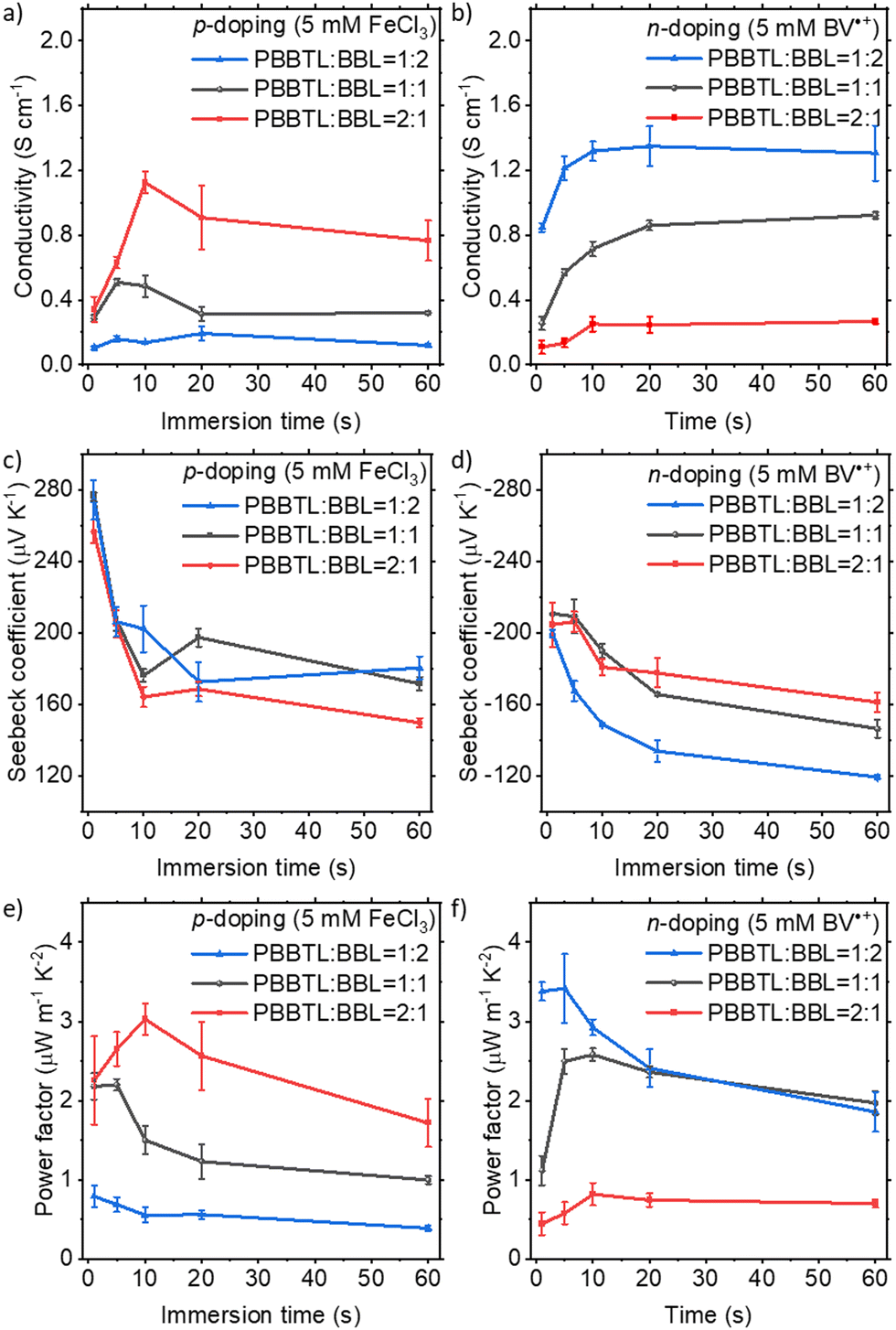 | ||
| Fig. 2 (a and b) Electrical conductivities, (c and d) Seebeck coefficients and (e and f) power factors of p-doped (a, c and e) and n-doped (b, d and f) PBBTL:BBL blend films as a function of immersion time. | ||
The Seebeck coefficient decreased with longer immersion times for both p- and n-doping for the most part (Fig. 2c and d). The positive and negative Seebeck coefficients obtained after FeCl3- and BV˙+-doping prove their p- and n-type behaviours, making this the first demonstration of an ambipolar BHJ OTE device. For all blend ratios and p-/n-doping, the power factor, a product of conductivity and the square of the Seebeck coefficient, generally reached a maximum at around 5–10 s of immersion (Fig. 2e and f). A maximum power factor of 3.03 ± 0.20 μW m−1 K−2 was achieved for a p-doped PBBTL:BBL 2:1 ratio at 10 s immersion and 3.42 ± 0.43 μW m−1 K−2 for a n-doped PBBTL:BBL 1:2 ratio at 5 s immersion. Not surprisingly, these values are again lower as compared to their p- and n-doped neat films (PBBTL, 7.73 ± 0.24 μW m−1 K−2; BBL, 4.85 ± 0.46 μW m−1 K−2), respectively. It is worth noting that the p- and n-doped conductivities achieved at a 1:1 blend ratio were quite well-balanced, with considerably higher power factors as compared to the recently reported ambipolar conjugated polymer.20
Taking advantage of the ambipolarity of the blend PBBTL:BBL film, we fabricate a full thermoelectric device consisting of single p- and n-channel legs using the PBBTL:BBL 1:1 ratio blend film as a proof of concept (Fig. 3a). The p- and n-channels were selectively p- and n-doped via immersion in their respective dopant solutions. To maximize an output power in thermoelectric devices, resistance matching of the p- and n-channel legs must be accounted. Taking this into consideration, the p- and n-channel legs were subjected to 1 s immersion each in the FeCl3 and BV˙+ solutions. After thermal annealing, the total resistance of the full device was about 120 kΩ. The current density and the power density plot of the full device subjected to a ΔT of 3 K were recorded (Fig. 3b). The open-circuit voltage of the full device could reach a value greater than 1.8 mV and the short-circuit current could reach almost 0.6 mA cm−2. The resulting maximum output power density of the full device reached 0.27 μW cm−2, operating at a voltage of 0.93 mV and a current density of 0.29 mA cm−2.
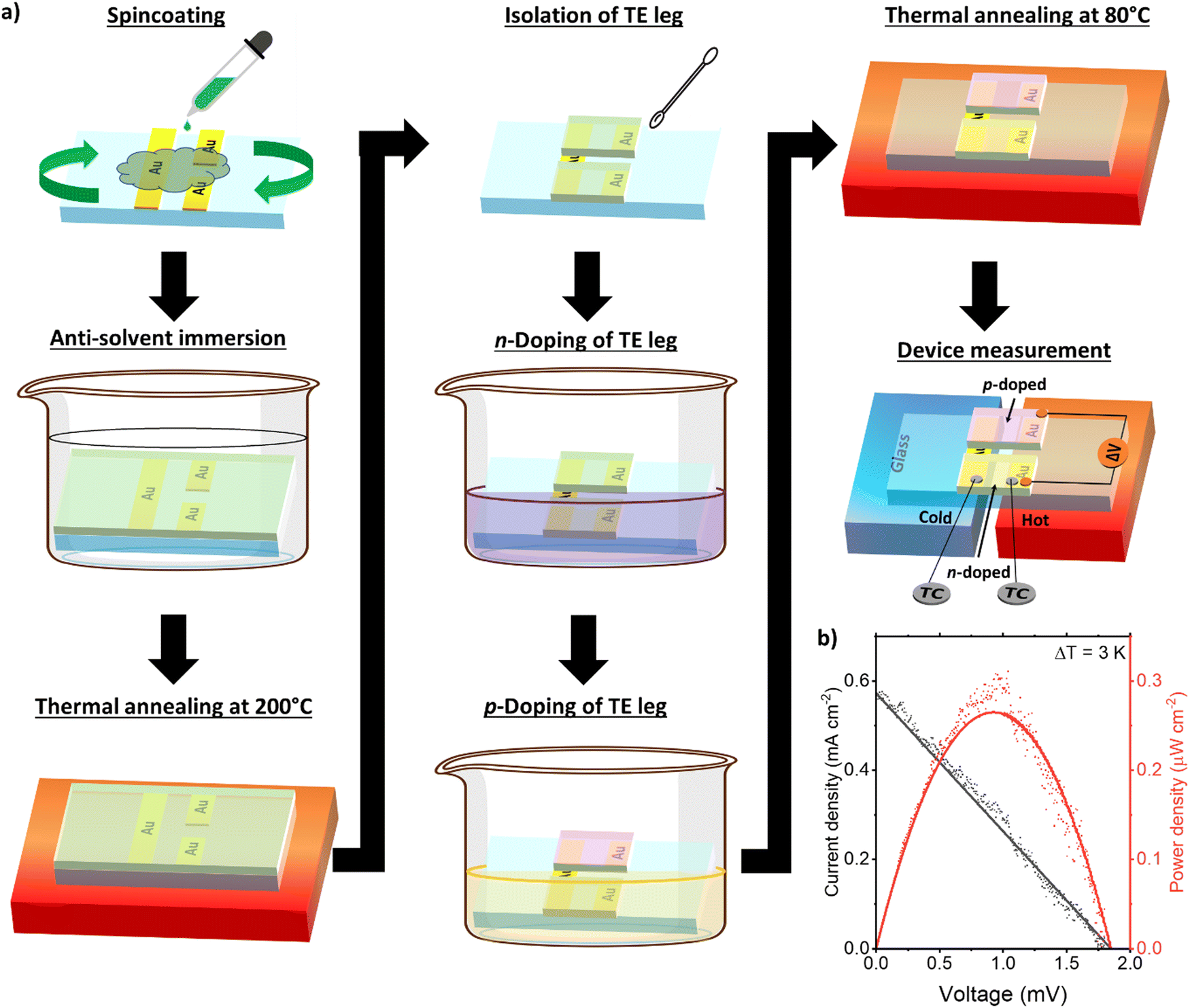 | ||
| Fig. 3 (a) Schematic of the full thermoelectric device fabrication using the PBBTL:BBL 1:1 ratio and 1 s immersion for both p- and n-doping. (b) J–V and power density plot of the full thermoelectric device at ΔT = 3 K. | ||
To understand the microstructure of the blend films, we first measured their GIWAXS (Fig. 4a and b). The pure PBBTL has a predominant face-on stacking with lamellar and π–π stacking distances of ∼5.5 Å (q = ∼1.15 Å−1) and ∼3.4 Å (q = ∼1.85 Å−1), respectively. BBL, on the other hand, has an edge-on stacking with lamellar and π–π stacking distances of ∼7.9 Å (q = ∼0.80 Å−1) and ∼3.4 Å (q = ∼1.82 Å−1), respectively. By considering the full width at half maximum of the π–π stacking peak for both pure polymers, one can tell that BBL is a more crystalline polymer than PBBTL. Going from the pure PBBTL to the PBBTL:BBL blend and to the pure BBL, we observed a gradual decrease of the PBBTL π–π stacking signal in the out-of-plane direction, with an increase of the BBL lamellar stacking signal. In the in-plane direction, a gradual increase of the BBL π–π stacking signal was also observed with an increasing BBL content. It also appears that BBL can better disrupt the microstructure of PBBTL but not vice versa, probably due to the higher crystallinity of the former. In UV-Vis absorbance and FTIR transmittance spectra, similar observations in terms of signal contribution can be made when the PBBTL:BBL ratio is changed (Fig. 4c and d). In these spectra, no significant shift could be observed, indicating no ground state electron transfer between the two polymers.
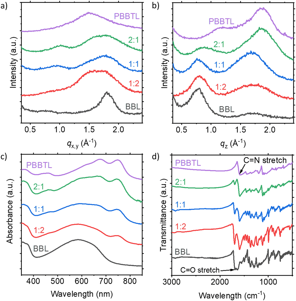 | ||
| Fig. 4 (a) In-plane and (b) out-of-plane GIWAXS of the pristine PBBTL and BBL films, as well as their blend films at different ratios. (c) UV-Vis absorbance and (d) FTIR transmittance spectra of pristine PBBTL and BBL films, as well as their blend films at different ratios. | ||
By using an atomic force microscopy-infrared (AFM-IR) technique, we mapped the morphology of the PBBTL:BBL blend films by scanning the samples at 1700 cm−1, which is characterized by C![[double bond, length as m-dash]](https://www.rsc.org/images/entities/char_e001.gif) O stretching that is present only in BBL (Fig. 5). First, all the blend ratios gave smooth films (Fig. 5a–c) with a low RMS value (∼10 nm) and this was supported by the scanning electron microscope (SEM) images (Fig. S1, ESI†). Smooth films are critical to provide reliable results for such characterization. Second, with a higher BBL content, i.e., a PBBTL:BBL ratio from 2:1 to 1:2, the blend films showed a stronger CO stretching signal (Fig. 5d–f). Third, the AFM height images of the blend films revealed porous nanostructures with dimensions of ∼50 nm, similar to those of the pure PBBTL and BBL films, as well as other ladder-type conjugated polymers.18,27,32 We attribute this to the film formation process, where the wet polymer films consisting of methanesulfonic acid (MSA)-swelled polymer networks shrink to form the porous nanostructures when the MSA leaches out during immersion in the anti-solvent. Thus, we believe that this should be universal to all (ladder) polymers processed in this manner. Fourth, the AFM-IR images also showed features with dimensions of ∼50 nm. While the positions of these features do not seem to match that of the AFM height images, they suggest that both PBBTL and BBL can be well-mixed on the nanoscale. In addition, the observed conductivities over a large channel length (0.25 cm) after p- and n-doping suggest the formation of percolation pathways that transverse well beyond the micron scale even though both PBBTL and BBL are well-mixed in the nanoscale. Lastly, to confirm the results, we performed selected area IR scans with different CO stretching intensities for the 1:1 film (Fig. 5g). We indeed observed higher CO stretching intensity ratios with respect to the CN stretching in areas with stronger CO signals, where the CN stretching is mainly contributed by PBBTL.
O stretching that is present only in BBL (Fig. 5). First, all the blend ratios gave smooth films (Fig. 5a–c) with a low RMS value (∼10 nm) and this was supported by the scanning electron microscope (SEM) images (Fig. S1, ESI†). Smooth films are critical to provide reliable results for such characterization. Second, with a higher BBL content, i.e., a PBBTL:BBL ratio from 2:1 to 1:2, the blend films showed a stronger CO stretching signal (Fig. 5d–f). Third, the AFM height images of the blend films revealed porous nanostructures with dimensions of ∼50 nm, similar to those of the pure PBBTL and BBL films, as well as other ladder-type conjugated polymers.18,27,32 We attribute this to the film formation process, where the wet polymer films consisting of methanesulfonic acid (MSA)-swelled polymer networks shrink to form the porous nanostructures when the MSA leaches out during immersion in the anti-solvent. Thus, we believe that this should be universal to all (ladder) polymers processed in this manner. Fourth, the AFM-IR images also showed features with dimensions of ∼50 nm. While the positions of these features do not seem to match that of the AFM height images, they suggest that both PBBTL and BBL can be well-mixed on the nanoscale. In addition, the observed conductivities over a large channel length (0.25 cm) after p- and n-doping suggest the formation of percolation pathways that transverse well beyond the micron scale even though both PBBTL and BBL are well-mixed in the nanoscale. Lastly, to confirm the results, we performed selected area IR scans with different CO stretching intensities for the 1:1 film (Fig. 5g). We indeed observed higher CO stretching intensity ratios with respect to the CN stretching in areas with stronger CO signals, where the CN stretching is mainly contributed by PBBTL.
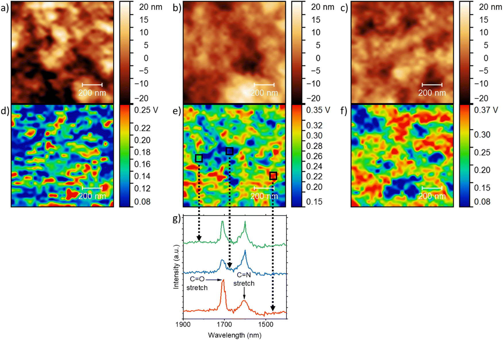 | ||
| Fig. 5 AFM height images of the PBBTL:BBL blend films at (a) 2:1, (b) 1:1 and (c) 1:2 ratios, and their corresponding AFM-IR images (d)–(f). AFM-IR images were scanned at 1700 cm−1, corresponding to the CO stretching in BBL, as the excitation energy. (g) IR absorbance in the 1900–1400 cm−1 range for three different regions (green, blue and red) in the PBBTL:BBL 1:1 blend film. | ||
The UV-Vis-NIR absorption spectra of the p- and n-doped polymer blend films are shown in Fig. 6. The spectra of the p-doped blends are normalized at the λmax for BBL at around 585 nm since BBL cannot be p-doped using FeCl3. Likewise, the spectra of the n-doped blends are normalized at λmax for PBBTL at around 747 nm since PBBTL cannot be n-doped using BV˙+. For these films, blends with higher p- or n-type polymer ratios resulted in a larger change in the UV-Vis-NIR absorption upon p- or n-doping, respectively. A significant change in the UV-Vis-NIR absorption was observed for all immersion times for p-doping in FeCl3 solution. In comparison with the pure PBBTL film, it appears that the addition of BBL in the blend films enables more efficient FeCl3 p-doping. However, there was no significant change in the UV-Vis-NIR absorption of the blend films after 1 s immersion in the BV˙+ n-dopant solution. And in comparison with the pure BBL film, it appears that the addition of PBBTL in the blend films impedes the BV˙+ n-doping process.
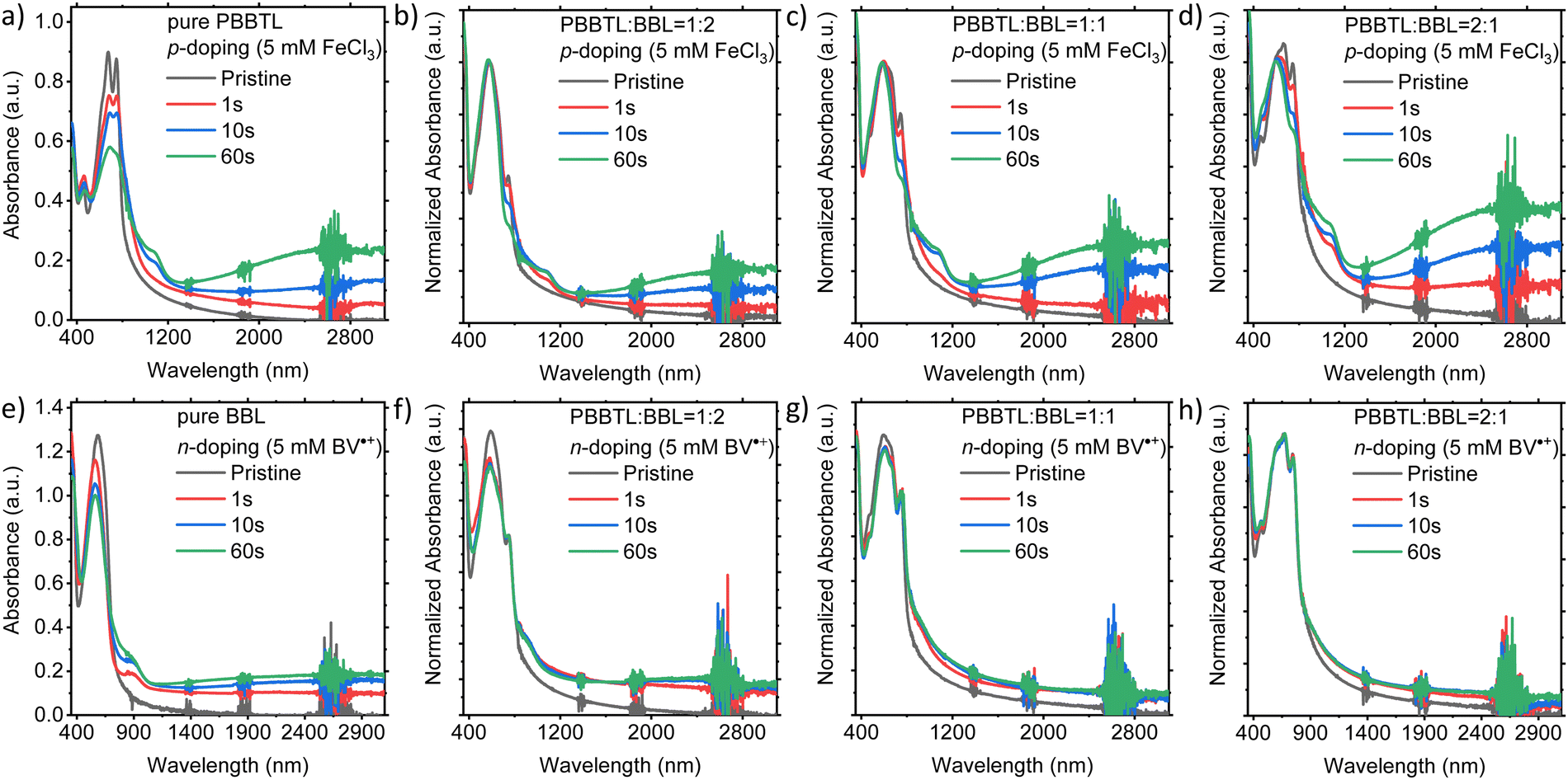 | ||
| Fig. 6 UV-Vis-NIR spectra of pure and blend films upon p- and n-doping. (a) Pure PBBTL with p-doping. PBBTL:BBL blend ratios (b) 1:2, (c) 1:1 and (d) 2:1 with p-doping. Absorbances in (b–d) are normalized at λmax for BBL at around 585 nm since BBL is unaffected by p-doping and the spectra overlap of BBL and PBBTL, to illustrate the increase in polaron absorption and the decrease in the neutral state absorption of PBBTL upon p-doping. (e) Pure BBL with n-doping. PBBTL:BBL blend ratios (f) 1:2, (g) 1:1 and (h) 2:1 with n-doping. Absorbances in (f–h) are normalized at λmax for PBBTL at around 747 nm since PBBTL is unaffected by n-doped and the spectra overlap of PBBTL and BBL, to illustrate the increase in polaron absorption and the decrease in the neutral state absorption of BBL upon n-doping. | ||
Conclusion
In an all-polymer BHJ system, the microstructure of one polymer is highly dependent on another, and how these polymers phase separate and crystallize strongly underlie their device performance.21,33,34 The extent of this effect depends on the relative crystallinity of the polymers, i.e., the polymer with lower crystallinity will have its microstructure more disrupted by the polymer with higher crystallinity, vice versa. In the case of the PBBTL:BBL blend, the polymers were well-mixed on the nanoscale according to AFM-IR analysis. PBBTL has a lower crystallinity than BBL and hence its microstructure is more disrupted. This larger disruption in the PBBTL's microstructure translates to a larger decrease in the thermoelectric performances of the p-doped blend films as opposed to the smaller disruption in the BBL's microstructure which translates to a smaller decrease in the n-doped blend films. Moreover, molecular dopants are known to impact the microstructures and device performance of polymer thermoelectrics.35–38 For example, using a similar doping process, FeCl3 was shown to be able to disrupt the crystallinity of PBBTL and other conjugated polymers.18,39 No disruption in π–π stacking could be observed for BV˙+-doped BBL.28 In some cases, enhancement in crystallinity was even observed in BV˙+-doped conjugated polymers.17,40 Consequently, the much higher p-type conductivities of PBBTL were appreciably counteracted by the negative impact of blend mixing and FeCl3-doping while the lower n-type conductivities of BBL were not so affected by blend mixing and BV˙+-doping. The result is well-balanced p- and n-doped conductivities for the PBBTL:BBL 1:1 blend ratio that enable the fabrication of a full thermoelectric device with both p- and n-channel legs using a single polymer film, simplifying the device fabrication process significantly. The obtained p- and n-doped conductivities were impressive given the fact that the device channel length was large and the polymers were well-mixed on the nanoscale, suggesting great potential for application in polymer micro-thermoelectric devices.
While the polymers and dopants used in this work are not new and the device performances of the BHJ polymer thermoelectrics are still relatively low, our work here demonstrates the possibility of using the BHJ donor–acceptor blend that can be either p- or n-doped. This is akin to the early stages of BHJ OPV research where known materials were used and power conversion efficiencies were low. However, since then, new science, new materials, new concepts, and research areas have sprung out from OPV research, with their power conversion efficiencies reaching almost 20% now, almost on par with silicon and perovskite solar cell technologies. Moreover, the science of BHJ polymer blend thermoelectrics is fundamentally different from that of BHJ OPV as the former involves chemical doping, thermoelectric effect, and conducting materials while the latter deals with the photovoltaic effect and semiconducting materials. There is much more to understand in this new system, and can benefit or give rise to new concepts/applications in the future.
Conflicts of interest
There are no conflicts to declare.Acknowledgements
T. L. D. T. and J. X. would like to acknowledge the A*STAR, SERC Thermoelectric Materials Program (grant numbers: 1527200019 and 1527200021) and the Agritech Program (grant numbers: A19D9a0096). Q. H. would like to acknowledge the Natural Science Basic Research Program of Shaanxi (Program No. 2019JLP-11) and the International Cooperation Training Program for Innovation Talents of China Scholarship Council for his funding support.References
- X. Guo, M. Baumgarten and K. Müllen, Prog. Polym. Sci., 2013, 38, 1832–1908 CrossRef CAS.
- J. Kim, M. Rémond, D. Kim, H. Jang and E. Kim, Adv. Mater. Technol., 2020, 5, 1900890 CrossRef CAS.
- G. Li, W.-H. Chang and Y. Yang, Nat. Rev. Mater., 2017, 2, 17043 CrossRef CAS.
- J. Yang, Z. Zhao, S. Wang, Y. Guo and Y. Liu, Chemistry, 2018, 4, 2748–2785 CrossRef CAS.
- W. T. Neo, Q. Ye, S.-J. Chuaa and J. Xu, J. Mater. Chem. C, 2016, 4, 7364–7376 RSC.
- Z. a Li, C.-C. Chueh and A. K.-Y. Jen, Prog. Polym. Sci., 2019, 99, 101175 CrossRef CAS.
- T. Leydecker, Z. M. Wang, F. Torricelli and E. Orgiu, Chem. Soc. Rev., 2020, 49, 7627–7670 RSC.
- A. Lund, N. M. v. d. Velden, N.-K. Persson, M. M. Hamedi and C. Müller, Mater. Sci. Eng., R, 2018, 126, 1–29 CrossRef.
- Z. Zhang, M. Liao, H. Lou, Y. Hu, X. Sun and H. Peng, Adv. Mater., 2018, 30, 1704261 CrossRef PubMed.
- S. Wang, G. Zuo, J. Kim and H. Sirringhaus, Prog. Polym. Sci., 2022, 129, 101548 CrossRef CAS.
- B. Russ, A. Glaudell, J. J. Urban, M. L. Chabinyc and R. A. Segalman, Nat. Rev. Mater., 2016, 1, 16050 CrossRef CAS.
- M. Campoy-Quile, Philos. Trans. R. Soc., A, 2019, 377, 20180352 CrossRef PubMed.
- S.-J. Wang, S. Wohlrab, H. Reith, D. Berger, H. Kleemann, K. Nielsch and K. Leo, Adv. Electron. Mater., 2022 DOI:10.1002/aelm.202200629.
- Q. Zhang, K. Deng, L. Wilkens, H. Reith and K. Nielsch, Nat. Electron., 2022, 5, 333–347 CrossRef.
- B. Derby, Annu. Rev. Mater. Res., 2010, 40, 395–414 CrossRef CAS.
- S. Moradi, N. Bandari, V. K. Bandari, F. Zhu and O. G. Schmidt, Adv. Mater. Technol., 2019, 4, 1900519 CrossRef CAS.
- T. L. D. Tam, T. T. Lin, M. I. Omer, X. Wang and J. Xu, J. Mater. Chem. A, 2020, 8, 18916–18924 RSC.
- T. L. D. Tam, M. Lin, S. W. Chien and J. Xu, ACS Macro Lett., 2022, 11, 110–115 CrossRef CAS.
- X. Wu, T. L. D. Tam, C. Shuai, T. Salim, X. Zhao, Z. Zhou, M. Lin, J. Xu, Y.-L. Loo and W. L. Leong, Adv. Mater., 2022, 34, 2206118 CrossRef CAS.
- Y. Chen, L. Zhao, P.-A. Chen, Y. Li, J. Guo, Y. Liu, X. Qiu, J. Xia, K. Chen, H. Chen, X. Lu, L. Jiang, L. Liao, T.-Q. Nguyen and Y. Hu, Matter, 2022, 5, 2882–2897 CrossRef CAS.
- G. Wang, F. S. Melkonyan, A. Facchetti and T. J. Marks, Angew. Chem., Int. Ed., 2019, 58, 4129–4142 CrossRef CAS PubMed.
- J. Sun, M.-L. Yeh, B. J. Jung, B. Zhang, J. Feser, A. Majumdar and H. E. Katz, Macromolecules, 2010, 43, 2897–2903 CrossRef CAS.
- G. Zuo, X. Liu, M. Fahlman and M. Kemerink, Adv. Funct. Mater., 2018, 28, 1703280 CrossRef.
- G. Zuo, Z. Li, E. Wang and M. Kemerink, Adv. Electron. Mater., 2018, 4, 1700501 CrossRef.
- G. Zuo, H. Abdalla and M. Kemerink, Adv. Electron. Mater., 2019, 5, 1800821 CrossRef CAS.
- O. Zapata-Arteaga, S. Marina, G. Zuo, K. Xu, B. Dörling, L. A. Pérez, J. S. Reparaz, J. Martín, M. Kemerink and M. Campoy-Quiles, Adv. Energy Mater., 2022, 12, 2104076 CrossRef CAS.
- T. L. D. Tam, M. Lin, A. D. Handoko, T. T. Lin and J. Xu, J. Mater. Chem. A, 2021, 9, 11787–11793 RSC.
- T. L. D. Tam, M. Lin, A. D. Handoko and J. Xu, ACS Appl. Polym. Mater., 2021, 3, 5596–5603 CrossRef CAS.
- S. Wang, H. Sun, U. Ail, M. Vagin, P. O. Å. Persson, J. W. Andreasen, W. Thiel, M. Berggren, X. Crispin, D. Fazzi and S. Fabiano, Adv. Mater., 2016, 28, 10764–10771 CrossRef CAS PubMed.
- C.-Y. Yang, M.-A. Stoeckel, T.-P. Ruoko, H.-Y. Wu, X. Liu, N. B. Kolhe, Z. Wu, Y. Puttisong, C. Musumeci, M. Massetti, H. Sun, K. Xu, D. Tu, W. M. Chen, H. Y. W. M. Fahlman, S. A. Jenekhe, M. Berggren and S. Fabiano, Nat. Commun., 2021, 12, 2354 CrossRef CAS PubMed.
- S. Wang, T.-P. Ruoko, G. Wang, S. Riera-Galindo, S. Hultmark, Y. Puttisong, F. Moro, H. Yan, W. M. Chen, M. Berggren, C. Müller and S. Fabiano, ACS Appl. Mater. Interfaces, 2020, 12, 53003–53011 CrossRef CAS.
- Q. He, T. L. D. Tam, T. T. Lin, S. W. Chien, M. Lin, H. Meng, W. Huang and J. Xu, ACS Macro Lett., 2022, 11, 1136–1141 CrossRef CAS.
- G. Wang, N. D. Eastham, T. J. Aldrich, B. Ma, E. F. Manley, Z. Chen, L. X. Chen, M. O. d. l. Cruz, R. P. H. Chang, F. S. Melkonyan, A. Facchetti and T. J. Marks, Adv. Energy Mater., 2018, 8, 1702173 CrossRef.
- E. F. Manley, J. Strzalka, T. J. Fauvell, T. J. Marks and L. X. Chen, Adv. Energy Mater., 2018, 8, 1800611 CrossRef.
- Z. Liang, Y. Zhang, M. Souri, X. Luo, A. M. Boehm, R. Li, Y. Zhang, T. Wang, D.-Y. Kim, J. Mei, S. R. Marder and K. R. Graham, J. Mater. Chem. A, 2018, 6, 16495–16505 RSC.
- J. M. Han, S. E. Yoon, K. H. Jung, O. Bae, D. Kim, U. Kim, H. Seo, F. S. Kim, K. C. Kim, J. H. Kim and B.-G. Kim, Chem. Eng. J., 2022, 431, 133779 CrossRef.
- M. Goel and M. Thelakkat, Macromolecules, 2020, 53, 3632–3642 CrossRef CAS.
- T. L. D. Tam and J. Xu, J. Mater. Chem. A, 2021, 9, 5149–5163 RSC.
- B. Li, X. Li, F. Yang, Y. Chen, X. Mao, S. Wan, H. Xin, S. Yan, M. Wang, C. Gao and L. Wang, ACS Appl. Energy Mater., 2021, 4, 4662–4671 CrossRef CAS.
- T. L. D. Tam and J. Xu, J. Mater. Chem. C, 2020, 8, 17261–17268 RSC.
Footnotes |
| † Electronic supplementary information (ESI) available. See DOI: https://doi.org/10.1039/d2tc03684c |
| ‡ Both authors contribute equally to the manuscript. |
| This journal is © The Royal Society of Chemistry 2023 |