
Twist angle can expand charge carrier diffusion length in bilayer black phosphorus: ab initio quantum dynamics†
Yonghao
Zhu
and
Run
Long
 *
*
College of Chemistry, Key Laboratory of Theoretical & Computational Photochemistry of Ministry of Education, Beijing Normal University, Beijing, 100875, P. R. China. E-mail: runlong@bnu.edu.cn
First published on 5th June 2023
Abstract
Focusing on bilayer black phosphorus (BP) and performing nonadiabatic molecular dynamic (NA-MD) simulations, we demonstrate that appropriate twist angles can significantly improve the charge carrier lifetime and diffusion length. Interlayer coupling is determined by the interlayer distance rather than wavefunction overlap between the two-layer BP. Compared to AB stacking, the weakened interlayer couplings, presented in the twisted systems, soften the interlayer breathing modes and inhibit the out-of-plane motions of P atoms by increasing the interlayer distances, which decreases NA coupling from the 38.94° to 11.54° system. Spontaneous charge separation happens in the 11.54° system due to the mismatched potentials of electrons and holes in high-symmetry stacking-induced moiré patterns, thereby generating the smallest NA coupling. Overall, non-adiabatic couplings (NACs) dominate nonradiative electron–hole recombination and extend the carrier lifetimes to 776 ps in the 38.94° and 1223 ps in the 11.54° system, which is one order of magnitude longer than that in the AB stacking. Correlating with the modulated charge carrier mobilities, the electron and hole diffusion lengths are extended by factors of 4.2 and 3.6 in the 11.54° system and 4.7 and 1.5 in the 38.94° system, compared with that in AB stacking. Our work provides atomic insights on twist angle-dependent carrier dynamics, including recombination and transport.
1. Introduction
Black phosphorus (BP) has emerged as a promising optoelectronic material against graphene and transition metal dichalcogenides (TMDs) because it simultaneously holds a direct layer-dependent bandgap,1,2 relatively high charge mobility,1,3 and large current on/off ratios.3,4 These advantages enable BP to exhibit great potential for the fabrication of advanced electronics and optoelectronics.5–7 Interfacing BP with other materials facilitates to drive exciton separation and delay charge recombination.8 The twist angle, firstly realized in graphene9 and TMDs,10 followed by BP,11 provides an additional degree of freedom to engineer the electrical properties and even the charge dynamics of the two-dimensional (2D) materials. The combination of twist and electronics spawned twistronics, which is an emerging discipline attracting a broad range of interests from chemists, physicists, and materials scientists.Modulating the high-symmetry stacking orders of bilayer BP can spontaneously lead to the formation of different moiré patterns when the twist angles are sufficient small,12 which was theoretically predicted to be energetically favorable by about 4 meV relative to AB stacking when the twist angle is 70.53°.13 The previous studies show that the uneven distribution of interlayer distance produces localized valence band maximum (VBM) and conduction band minimum (CBM) states in twisted bilayer BP,12,14 particularly in small-enough twisted angles, which act as impurities to reduce carrier mobilities.12 Furthermore, the wavefunction overlap in the interlayer regions puzzle the relationship between interlayer coupling and distance, which are regarded as features of strengthening interactions between two layers.12,15 Experiments have demonstrated that slight blue shifts in the Raman vibrational peaks of the A1g and A2g modes are exhibited in bilayer BP due to the strong interlayer coupling,15 which results in the vanishing of electronic polarization along the vertical direction.16 This may modulate the electronic–vibrational interactions that affect the elastic and inelastic electron–phonon scattering and hence influence the charge carrier lifetime.10,17–19 The product of charge carrier lifetime and mobility equals carrier diffusion length, which plays a crucial role in determining the performance of photoelectric devices. Higher carrier mobility and longer carrier lifetime produce larger carrier diffusion length and better device performance, such as photodetectors and photocatalysts.20,21 However, the influence of the twist angles, which affect the electronic structures and interlayer couplings, on the charge carrier lifetime and diffusion length has not been theoretically explored. This requires a combination of a time-domain simulation22,23 for the lifetimes and deformation potential theory24 for the latter. An understanding of the charge recombination and carrier diffusion length influenced by the twisted angles leads to useful and often critical insights into phonon-assisted electron dynamics and provides guidelines for material design and improvement.
To study the influence of twist angle on electron–hole recombination and transport in bilayer BP, we created AB stacking, 38.94°, and 11.54° configurations without introducing any additional strain. The twist angles significantly affect interlayer couplings and charge localizations, which manage the nonradiative electron–hole recombination. Interlayer coupling is almost linearly dependent on the interlayer distance, which is irrelevant to wavefunction overlap in the bilayer BP. The overlaps of CBM wavefunctions in the interfacial regions favor charge transport, and the overlap originates from the same sign wavefunctions of the top- and bottom-layer BP correlated with the faced P atom arrangements. Compared to AB stacking, interlayer couplings become weaker in twisted systems due to the increased interlayer distances and softened interlayer breathing modes, thereby decreasing the NACs by inhibiting the breathing motions of P atoms. In the 11.54° system, the mismatched potentials of electrons and holes in the high-symmetry stackings are responsible for charge separation on different moiré patterns, which serves to decrease NAC and nonradiative charge recombination further and favors directional charge transport. As a consequence, the charge carrier lifetimes are extended to776 ps in the 38.94° system and 1223 ps in the 11.54° system from 160 ps in AB stacking. The electrons and holes diffusion lengths, which are associated with the modulated charge mobilities, increase by factors of 4.2 and 3.6 in the 11.54° system and 4.7 and 1.5 in the 38.94° system, compared to those in AB stacking. The prolonged charge carrier lifetime and diffusion lengths are beneficial for improving the performance of BP-based optoelectronics and photovoltaics. Our simulations establish the microscopic mechanisms for twist angle-dependent interlayer coupling, electronic structures, charge recombination dynamics, and carrier transport at the atomic level and in the time-domain.
2. Simulation details
The nonadiabatic molecular dynamics (NA-MD) simulation of the phonon-assisted nonradiative electron–hole recombination was performed using the decoherence-induced surface hopping (DISH) algorithm25 implemented within the PYXAID code26,27 on top of time-dependent Kohn–Sham density functional theory (TD-DFT).22,23 The DISH algorithm incorporates decoherence correction in the current classical-quantum hybrid dynamics. In this approach, the electrons and nuclei are treated quantum mechanically and classically, respectively.22,23 The method has been proven robust to study photoinduced carrier dynamics for a variety of systems, including perovskites,28–30 metal oxides,31,32 and 2D materials.10,33–35 The detailed description of the theoretical approach can be found in previous works.26,27 The simulation details are provided in the ESI.†3. Results and discussion
3.1 Geometric and electronic structures
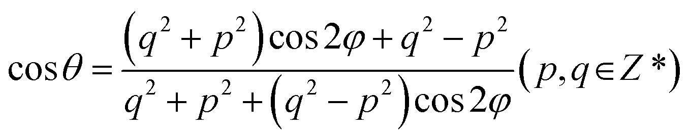
Fig. 1 shows the optimized geometries of AB stacking, 38.94°, and 11.54° systems. To eliminate the size effect on the charge dynamics, the supercells of AB stacking and 38.94° were expanded to make the number of atoms same as that in the 11.54° system. The AB stacking is the most stable in energy, compared with other high-symmetry stackings.36 The twisted BPs are constructed using the coincidence-site lattice (CSL) method.13 The twist angle, θ, is defined as follows.Here, φ is related to lattice vectors of BP and is calculated based on tan
![[thin space (1/6-em)]](https://www.rsc.org/images/entities/char_2009.gif) φ = a1/a2 = 1.4142,13 where a1 and a2 are the lattice constants of primitive cell of BP. This method does not introduce additional strain, which notably affects the bandgaps of BP.37 Generally, larger p and q values generate smaller twist angles and larger superlattices (Fig. S1†). To limit the number of atoms, the twisted models are constructed by varying q with a fixed p = 1. Both the AB stacking (Fig. 1a) and 38.94° (Fig. 1b) systems do not form moiré patterns, which is formed in the 11.54° system due to the high-symmetry patterns of AB, AA, AB′, and AA′ stacking (Fig. 1c). Playing key roles in nonradiative recombination, interlayer couplings and charge localizations were determined by the moiré patterns formed by the four high-symmetry stackings, while previous studies showed that interlayer coupling is dominated by the distance between the two layers rather than wavefunction overlap in TMDs, where a smaller interlayer distance favors larger coupling.38,39 Therefore, it necessitates exploring the accurate relationships between the interlayer coupling and the distance as well as the wavefunction overlaps in high-symmetry stackings and twisted bilayer BP.
φ = a1/a2 = 1.4142,13 where a1 and a2 are the lattice constants of primitive cell of BP. This method does not introduce additional strain, which notably affects the bandgaps of BP.37 Generally, larger p and q values generate smaller twist angles and larger superlattices (Fig. S1†). To limit the number of atoms, the twisted models are constructed by varying q with a fixed p = 1. Both the AB stacking (Fig. 1a) and 38.94° (Fig. 1b) systems do not form moiré patterns, which is formed in the 11.54° system due to the high-symmetry patterns of AB, AA, AB′, and AA′ stacking (Fig. 1c). Playing key roles in nonradiative recombination, interlayer couplings and charge localizations were determined by the moiré patterns formed by the four high-symmetry stackings, while previous studies showed that interlayer coupling is dominated by the distance between the two layers rather than wavefunction overlap in TMDs, where a smaller interlayer distance favors larger coupling.38,39 Therefore, it necessitates exploring the accurate relationships between the interlayer coupling and the distance as well as the wavefunction overlaps in high-symmetry stackings and twisted bilayer BP.
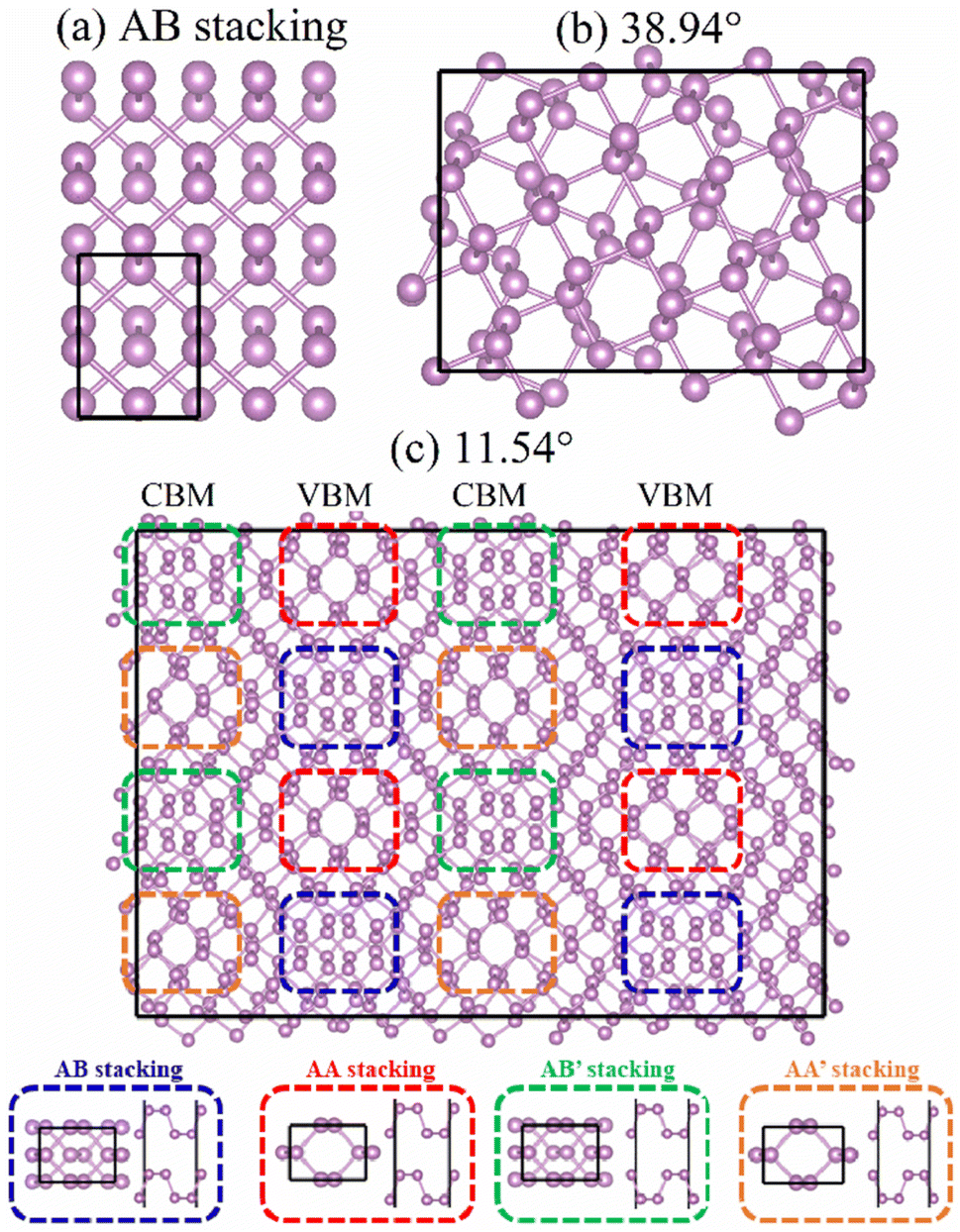 | ||
| Fig. 1 Geometries of bilayer BP with (a) AB stacking, (b) 38.94°, and (c) 11.54° twist angles. The 11.54° twist angle system forms obvious moiré patterns, which are constituted by four high-symmetry patterns, including AB (dashed blue block), AA (dashed red block), AB′ (dashed green block), and AA′ (dashed orange block) stackings. The images were created by VESTA.40 | ||
Bearing this in mind, we manually modulated the interlayer distance and calculate the single point energy and bandgap for high-symmetry stackings (Fig. 2a and S2a†) and twisted systems (Fig. 2b and S2b†), respectively. With the interlayer distance increasing, the interactions between the two layers gradually disappear and the bandgaps increase correspondingly (Fig. S2 and S3a†). In high-symmetry stackings, AB stacking exhibits the strongest interaction energy, followed by AB′, AA, and AA′ stackings (Fig. 2a), and the interlayer distance follows this order (Table S1†). The findings suggest that the interlayer couplings in bilayer BP are almost linearly dependent on the interlayer distance.41,42 In twisted systems, the interaction energy of bilayer BP is converged to about 0.3 eV per unit cell regardless of the twist angle when it is approaching to 26.53° and therefore exhibits close interlayer distance (Fig. 2b and Table S2†). In general, a smaller twist angle leads to more explicit moiré patterns compared to a larger twist angle. Hence, we chose the 11.54° twist angle system for studying the charge dynamics.
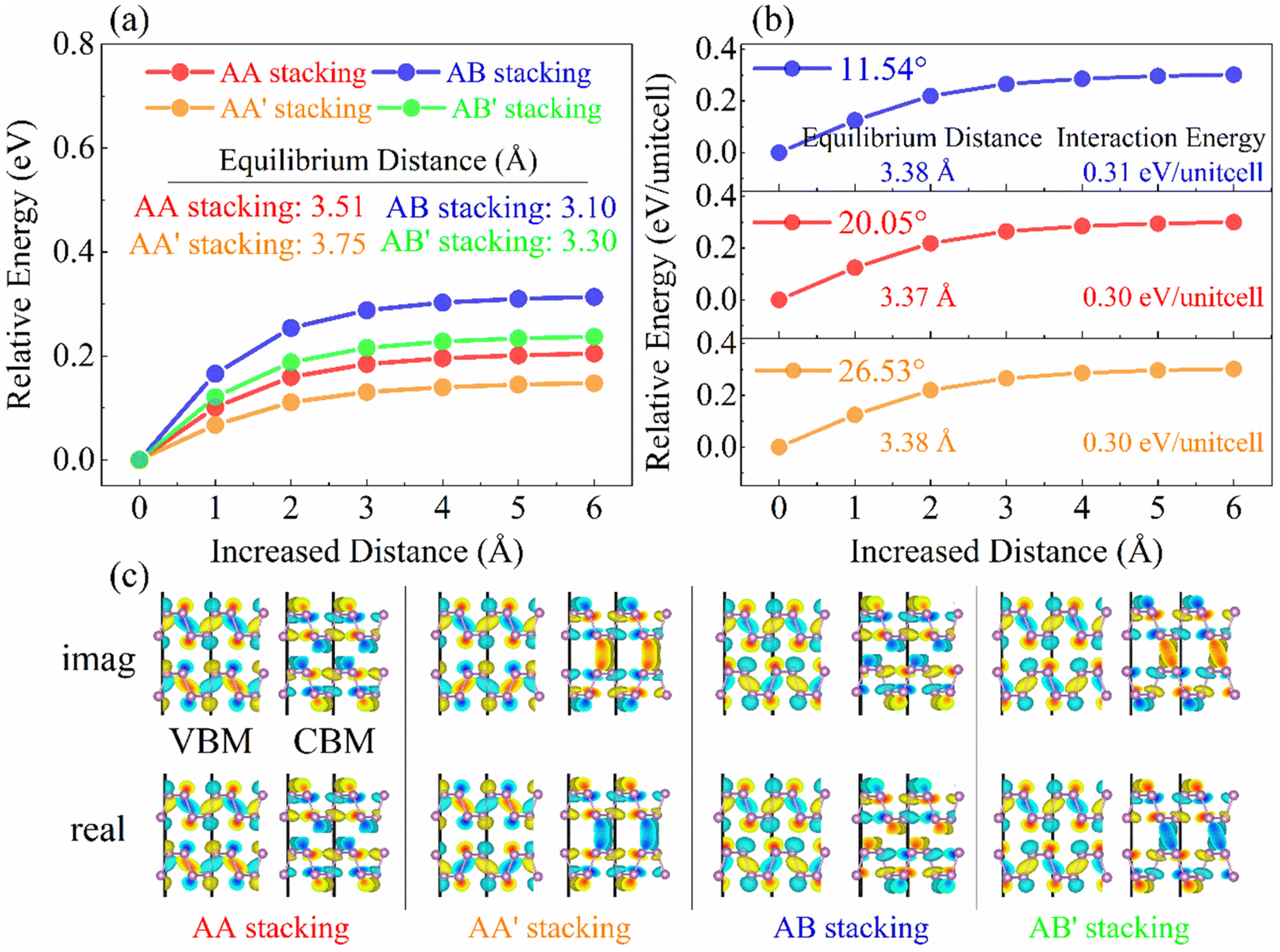 | ||
| Fig. 2 The interlayer distance-dependent total energy difference in (a) high-symmetry stackings (calculated by VASP) and (b) twisted systems (calculated by CP2K). The AB stacking shows the largest interaction energy and the shortest equilibrium distance (Table S1†) among four stackings, suggesting strongest interlayer coupling. In the twisted systems, the interlayer couplings are independent of the angles until it is lower than 38.94° (Table S2†). (c) Imaginary (imag.) and real components of the VBM and CBM wavefunctions in high-symmetry stackings. | ||
To explore how wavefunction overlap affects interlayer coupling, we computed the VBM and CBM wavefunctions, which were split into contribution to imaginary (imag.) and real components (Fig. 2c), where they do not overlap between the top and bottom layers in the AA and AB stackings. This feature remains true for the imaginary and real components of the VBM in the AA′ and AB′ stackings. However, the imaginary and real components of the CBM wavefunctions mix between the two BP layers in the two stackings, leading to the tails of the wavefunctions delocalizing onto the interlayer regions (Fig. 2c and S4†). Thus, wavefunction overlap does not affect the interlayer coupling, which is dominated by the interlayer distance. The overlap originates from the features of the CBM wavefunctions and faced arrangements of P atoms. First, the same sign wavefunctions of the two BP layers are the prerequisites for overlap. This is true for the CBM (same color) and does not hold for the counterpart VBM (different colors) for all the four high-symmetry stackings. Second, the faced arrangements of P atoms in the AA′ and AB′ stackings favor the interactions between lone-pair electrons and wavefunctions mixing, while the displaced P atoms between the top- and bottom-layer BP are against the interactions and overlap. The observations can also be applied to rationalize the overlap of the CBM wavefunctions of larger twisted angle systems, such as 70.53° and 55.88° (Fig. S5†).
Interlayer coupling has an influence on the out-of-plane vibrations of P atoms and further alters electron–phonon interaction. The average interlayer distances in the AB stacking, 38.94°, and 11.54° systems grows from 3.21 Å to 3.37 Å and 3.38 Å at 0 K, due to which the faced arrangements of P atoms strengthen the repulsive interactions between the lone pair of electrons in the twisted systems.16 Thermal fluctuations weaken the interlayer interaction, thereby increasing the distance to 3.25, 3.41, and 3.40 Å at 300 K. The smaller interlayer distance suggests stronger interaction, e.g., the AB stacking, also reflected by the much stronger interlayer distance fluctuations (Fig. 3a). The Fourier transforms (FTs) of the interlayer distance fluctuation give a peak at 50 cm−1 (Fig. 3b), which agrees well with the accurate calculations of phonon dispersion in high-symmetry stackings of layered BP with unit cell42 and can be assigned to the layer breathing mode (LBM).42 This mode modulates the interlayer separation and interaction, thus regulating the NACs and charge carrier lifetime. The magnitude of the LBM in AB stacking is significantly larger than that in twist systems, thus reflecting the strongest electron–vibrational interactions. The canonically-averaged standard deviation can quantify the extent of thermal motions of P atoms,43 which is calculated to be 0.60 Å for AB stacking, 0.42 Å for 38.94°, and 0.46 Å for 11.54°, according to 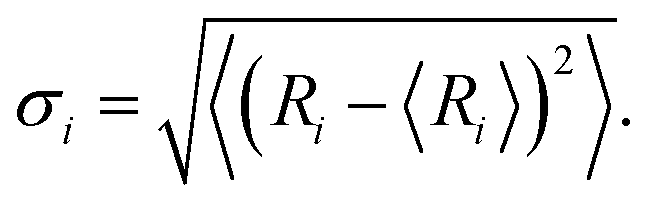 29,31 Here, Ri represents the location of atom i, and the angular bracket indicates ensemble averaging. Compared to twisted systems, the distinctly larger standard deviation of AB stacking explains the much stronger fluctuations of P atoms and electron–vibrational interaction, resulting in larger NACs and shorter decoherence time.
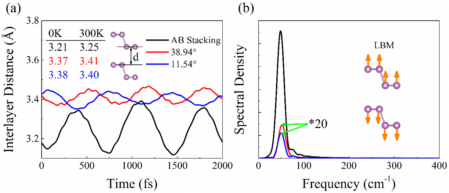 | ||
| Fig. 3 (a) Evolution of interlayer distance in bilayer BP with AB stacking, 38.94°, and 11.54° twist angles. (b) Spectral density obtained using Fourier transforms of the distance in (a). The peak located at about 50 cm−1 associated with the low-frequency out-of-plane vibration corresponds to LBM in Raman spectroscopy.45 The stronger fluctuation of the interlayer distance leads to the higher intensity of the LBM in the AB stacking. | ||
The calculation of phonon dispersion and electron–phonon coupling matrix is too expensive to be applied on systems of the current size, i.e., 792 atoms for the 11.54° system. To date, the literature shows that calculations of electron–phonon matrix have been performed only up to systems with 50 atoms.44 In the current method, the NACs and decoherence times are calculated, which correspond to the inelastic and elastic electron–phonon scatterings, respectively. The larger NACs and a shorter decoherence/pure-dephasing time characterize stronger electron–phonon scatterings, which lead to faster electron–hole recombination.
Fig. 4 shows the density of states (DOS) and the charge densities of the VBM and CBM. The DOS is splitting into contribution to the top- and bottom-layer BP. The 0.48 eV bandgap derived from the PBE functional for the AB stacking was scaled to 1.30 eV by adding a constant (Fig. 4a) according to the GW calculated46 and experimental values.47,48 The same constant was applied to the 38.94° and 11.54° systems, resulting in bandgaps of 1.39 eV (Fig. 4b) and 1.21 eV (Fig. 4c), respectively. The PBE functional is well known to contain the spurious self-interaction error inherently, which underestimates the bandgaps of materials, including BP. Hybrid functionals or a GW calculation46 can lead to the accurate bandgap of BP, which agrees well with the experimental value.47,48 However, hybrid functionals for periodic systems are too expensive to be used with NA-MD on systems with the current size. Therefore, we are limited by the available computing resources to the PBE level. The approach has previous studies on phonon-assisted electron–hole recombination in various systems, such as BP,33,49,50 metal halide perovskites,51–54 and metal oxides.31,55
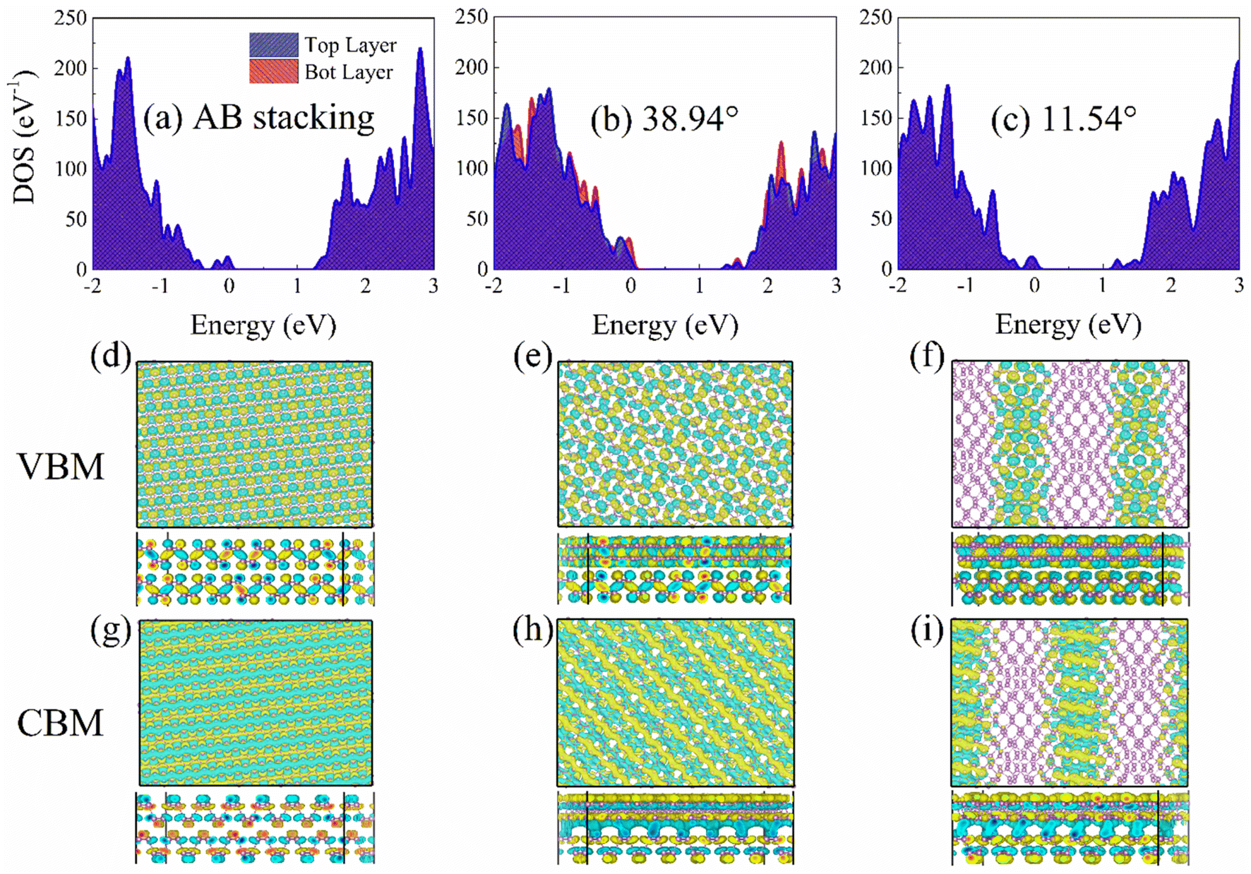 | ||
| Fig. 4 Electronic structures. Density of states (DOS) of bilayer BP for (a) AB stacking, (b) 39.84°, and (c) 11.54° twist angles, calculated using the CP2K package.56 The contributions to the DOSs are separated into the top and bottom-layer BP. The Fermi level is set to zero. (d–i) Charge densities of VBM and CBM of bilayer BP. The mismatched potentials separate the electron and hole in the 11.54° system (Fig. S7†), reducing NA coupling. | ||
The overlap of electron and hole wavefunctions, 〈ΨCBM|∇R|ΨVBM〉, determines the NA coupling. The charge densities of the VBM and CBM are almost uniformly distributed on the top- and bottom-layer BP in the AB stacking (Fig. 4d and g) and 38.94° (Fig. 4e and h) systems, which is associated with decreased overlap from the former to the latter, thus leading to NA coupling of 9.36 and 8.12 meV. In the 11.54° system, the VBM (Fig. 4f) is localized on the AB and AA patterns, while the CBM (Fig. 4i) resides on the AB′ and AA′ patterns,12,14 which remains constant at room temperature (Fig. S6†) and decreases the NAC to 2.92 meV. The spontaneous charge separation and localization arises from the potential mismatch of CBM and VBM in the high-symmetry stackings instead of the uneven distribution of interlayer distance (Table S1†). The CBM potentials in AB′ and AA′ stackings are lower, and the VBM potentials in AB and AA stackings are higher (Fig. S7†).
The performance of photovoltaics and optoelectronics is significantly dependent on charge carrier mobility. Therefore, we calculated the stacking-dependent carrier mobility according to the deformation potential theory24 and summarized the data in Table 1. The detailed method is given in ESI,† where the mobilities are determined by the effective mass, deformation potentials, and elastic modulus.24,57 The calculated hole and electron mobilities of 502 cm2 V−1 s−1 and 87 cm2 V−1 s−1 in the AB stacking system are in the 100 to 3000 cm2 V−1 s−1 range reported experimentally.1,3,36,57–59 In case of the 38.94° system, the electron mobility increases to 398 cm2 V−1 s−1 while the hole mobility goes down to 221 cm2 V−1 s−1. When the twist angle is reduced to 11.54°, the mobilities of negative and positive charges correspondingly change to 203 and 866 cm2 V−1 s−1. It seems that the twist angles are always beneficial for enhancing the electron mobility, which does not hold for hole mobility. The fact can be rationalized by the mixing of electron wavefunctions (Fig. 4f and i) other than hole wavefunctions (Fig. 4e and h) in the twisted systems. The mixing along the moiré patterns favors electron directional transport, thereby increasing the mobility. The calculated twist angle-dependent effective mass (EM) of electrons and holes shows no regularity compared to the AB stacking. The finding suggests that a rational control of twist angle can improve charge mobilities and advances the established understanding of small enough twist angles tending to act as impurities for carrier transport.12
| Systems | Hole EM | Hole mobility | Electron EM | Electron mobility |
|---|---|---|---|---|
| AB stacking | 0.12 | 502 | 0.13 | 87 |
| 38.94° | 0.20 | 221 | 0.14 | 398 |
| 11.54° | 0.12 | 866 | 0.22 | 203 |
3.2 Electron–vibrational interaction
Electron–vibrational interaction causes both elastic and inelastic electron–phonon scattering. The former destroys the coherence formed between the initial and final electronic states, and the latter creates the phonon modes coupled to the electronic subsystem and generates NACs. Both types of scattering affect charge carrier lifetime.The influence spectra (Fig. 5a), obtained from the Fourier transforms (FTs) of bandgap fluctuations (Fig. S8†), demonstrate that frequencies below 700 cm−1, including one low and three high frequency modes, are responsible for creating NACs and leading to electron–hole recombination. The major low-frequency peak at about 50 cm−1 in the AB stacking, belonging to LBM,45 is stronger than that in the twisted systems, agreeing with the amplitude of interlayer distance fluctuation (Fig. 3a). The dominant high-frequency peak at about 340 cm−1 can be attributed to the out-of-plane vibration of P–P bonds, A1g mode.45,48 Compared to the AB stacking, the peak intensities of twisted systems are lower, particularly for the 11.54° system, which indicates the suppressed out-of-plane vibration of P atoms. The peaks at about 408 and 460 cm−1 are assigned to in-plane P atoms motion, B2g and A2g modes, which have marginal contribution to NA coupling because they do not modulate the interlayer distance.
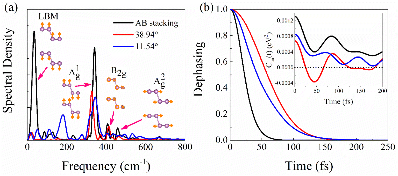 | ||
| Fig. 5 (a) Spectral densities obtained using Fourier transforms of the un-ACF of the bandgap fluctuations and (b) pure-dephasing functions. The inset of (b) shows the un-ACF, Cun(t), whose starting value equals the bandgap squared. The larger initial value generally leads to faster pure-dephasing. | ||
The decoherence time can be estimated as the pure-dephasing time of the optical response theory.60 Decoherence plays an important role in influencing the charge recombination dynamics.29 Generally, faster decoherence induces slower quantum dynamics, as exemplified by the quantum Zeno effect.61 Within second-order cumulant approximation, the pure-dephasing function,  is determined by the unnormalized autocorrelation functions (un-ACF) of the bandgap fluctuation (Fig. S8†).62Fig. 5b displays the pure-dephasing functions and un-ACFs (inset) for the three systems. Fitting pure-dephasing functions to a Gaussian, exp(−0.5 × (t/τ)2), gives the pure-dephasing time, τ, which is listed in Table 2. The dephasing times of AB stacking, 38.94°, and 11.54° are 21, 50, and 40 fs, respectively. The separated electron and holes tend to decrease the dephasing time,63 but AB stacking shows the largest phonon-induced energy gap fluctuation (Fig. S8†). The coherence loss is accelerated when a stronger amplitude of phonons couple to the electrons, for larger energy gap fluctuation.64 The un-ACF, Cij(t) = 〈δEij(t′)δEij(t − t′)〉t′, is the kernel of pure-dephasing function Dij(t). The term δEij(t) presented in the un-ACF corresponds to the phonon-induced fluctuation of the energy gap. The initial value δE2ij(0) equals to the energy gap fluctuation squared, with a larger initial value of the un-ACF and a shorter pure-dephasing time. As shown in the inset of Fig. 5b, the initial value of the un-ACF decreases in the sequence AB > 11.54° > 38.94°. Therefore, the pure-dephasing time decreases as AB < 11.54° < 38.94°. Furthermore, the calculated canonically averaged standard deviation, quantifying the extent of thermal motions of P atoms, is 0.6 Å for AB stacking, 0.42 Å for 38.94, and 0.46 Å for 11.54°, which also provides an additional source for the pure-dephasing times reported in the three systems. Therefore, the weaker motions of P atoms induced by twist angles lead to longer pure-dephasing times in the 38.94° and 11.54° systems.
| Systems | Bandgap | NAC | Dephasing | Recombination |
|---|---|---|---|---|
| AB stacking | 1.30 | 9.36 | 21 | 160 |
| 38.94° | 1.39 | 8.12 | 50 | 776 |
| 11.54° | 1.21 | 2.98 | 40 | 1223 |
3.3 Charge carrier lifetime and diffusion length
Fig. 6a presents the evolution of the first excited-state (CBM) populations in the three systems, representing nonradiative electron–hole recombination. Population decay is obtained using the method in the simulation details of ESI.† The recombination timescales summarized in Table 2 are obtained by fitting the data to P(t) = exp(−t/τ). The electron–hole recombination happens within 160 ps in the AB stacking, agreeing well with the experiments.65,66 Twist angles slow down the recombination, e.g., 776 ps for the 38.94° and 1223 ps for the 11.54° system. As shown in Table 2, the recombination timescales are dominated by the NAC, which successfully competes with the bandgap and pure-dephasing time. Compared with AB stacking, the decreased interlayer couplings (Fig. 3) and separated charge densities (Fig. 4f and i) lead to smaller NACs in the twisted systems. Slow nonradiative electron–hole recombination minimizes charge and energy losses and facilitates high-performance optoelectronics and photovoltaics.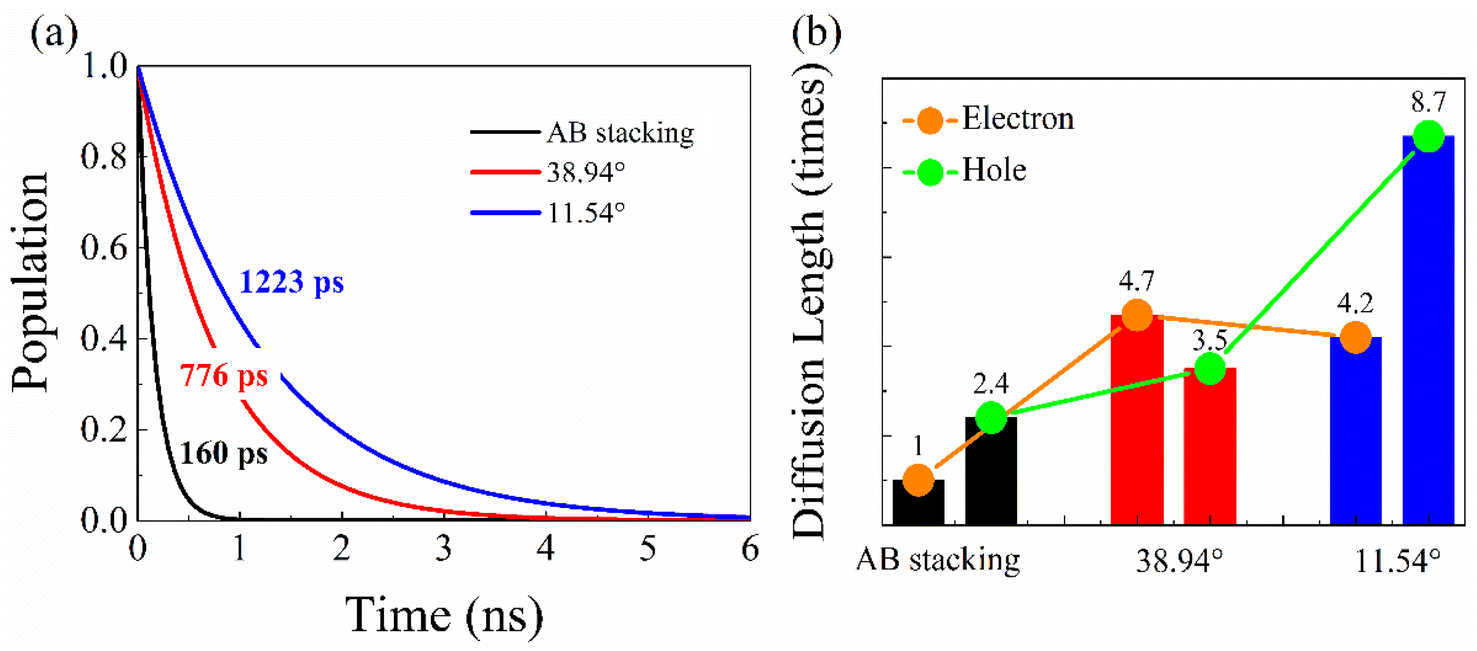 | ||
| Fig. 6 (a) Nonradiative electron–hole recombination dynamics in AB stacking, and bilayer BP with 38.94° and 11.54° twist angles. (b) The relationship between the charge carrier diffusion length and the stacking configurations. The diffusion lengths increase in the systems with twist angles, which extends the charge carrier lifetimes by decreasing the NACs. The electron diffusion length of AB stacking is set to 1. | ||
The diffusion length of the carrier, 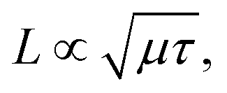 is crucial to the photoelectric devices.20,21 Higher carrier mobility, μ, and longer lifetime, τ, favor increasing diffusion length and device performance. The diffusion length increases as the twist angel grows (Fig. 6b). The L of the 38.94° and 11.54° systems is increased by factors of 4.7 and 4.2, relative to the AB stacking for electron, and 1.5 and 3.6 times for hole. Therefore, the smaller twist angle system, e.g., 11.54°, has better performance than the 38.94° and AB stacking systems, providing a rational strategy to design high performance BP or even TMDs-based optoelectronics and photovoltaics.
4. Conclusion
To sum up, we have investigated twist angle-dependent charge carrier lifetime and diffusion length in bilayer BP by simulating the nonradiative electron–hole recombination using a combination of TDDFT and NA-MD. The simulations indicate that interlayer coupling is dominated by the interlayer distance rather than the wavefunctions overlap. The same sign wavefunctions of the top- and bottom-layer BP, which are correlated with the faced P atom arrangements, delocalize charge into the interfacial regions and favor charge transport. The weakened interlayer couplings in the twisted systems soften the interlayer breathing modes and inhibit the motions of P atoms, which result in smaller NACs than that in AB stacking. In the 11.54° twisted system, the mismatched potentials between the electrons and holes in the high-symmetry stacking-induced moiré patterns separate positive and negative charges spontaneously, thereby reducing NAC and slowing down the nonradiative electron–hole recombination compared to the AB stacking and 38.94° systems. Driven by the layer breathing mode and the out-of-plane P–P bond vibration, A1g mode, the recombination is completed within 160 ps in the AB stacking and is prolonged to 776 and 1223 ps when the twist angles go down to 38.94° and 11.54°, respectively. Correspondingly, the electron and hole diffusion lengths increase significantly, up to factors of 4.2 and 3.6 in the 11.54° system and 4.7 and 1.5 in the 38.94° system. The obtained results provide valuable insights on extending the charge carrier lifetime and diffusion length of multiple BP by twist engineering, and the strategy can be applied to other layered materials, such as GeS and GeSe.Conflicts of interest
The authors declare no competing financial interest.Acknowledgements
This work was supported by the National Science Foundation of China (grant no. 21973006). R. L. acknowledges the Beijing Normal University Startup Package.References
- H. Liu, A. T. Neal, Z. Zhu, Z. Luo, X. Xu, D. Tománek and P. D. Ye, Phosphorene: An Unexplored 2D Semiconductor with a High Hole Mobility, ACS Nano, 2014, 8, 4033–4041 CrossRef CAS PubMed.
- S. Das, W. Zhang, M. Demarteau, A. Hoffmann, M. Dubey and A. Roelofs, Tunable Transport Gap in Phosphorene, Nano Lett., 2014, 14, 5733–5739 CrossRef CAS PubMed.
- L. Li, Y. Yu, G. J. Ye, Q. Ge, X. Ou, H. Wu, D. Feng, X. H. Chen and Y. Zhang, Black phosphorus field-effect transistors, Nat. Nanotechnol., 2014, 9, 372–377 CrossRef CAS PubMed.
- H. Hu, Z. Shi, K. Khan, R. Cao, W. Liang, A. K. Tareen, Y. Zhang, W. Huang, Z. Guo, X. Luo and H. Zhang, Recent advances in doping engineering of black phosphorus, J. Mater. Chem. A, 2020, 8, 5421–5441 RSC.
- S. K. Muduli, E. Varrla, Y. Xu, S. A. Kulkarni, A. Katre, S. Chakraborty, S. Chen, T. C. Sum, R. Xu and N. Mathews, Evolution of hydrogen by few-layered black phosphorus under visible illumination, J. Mater. Chem. A, 2017, 5, 24874–24879 RSC.
- N. Fu, C. Huang, P. Lin, M. Zhu, T. Li, M. Ye, S. Lin, G. Zhang, J. Du, C. Liu, B. Xu, D. Wang and S. Ke, Black phosphorus quantum dots as dual-functional electron-selective materials for efficient plastic perovskite solar cells, J. Mater. Chem. A, 2018, 6, 8886–8894 RSC.
- Z. Wu, J. Qi, W. Wang, Z. Zeng and Q. He, Emerging elemental two-dimensional materials for energy applications, J. Mater. Chem. A, 2021, 9, 18793–18817 RSC.
- Z.-K. Shen, Y.-J. Yuan, P. Wang, W. Bai, L. Pei, S. Wu, Z.-T. Yu and Z. Zou, Few-Layer Black Phosphorus Nanosheets: A Metal-Free Cocatalyst for Photocatalytic Nitrogen Fixation, ACS Appl. Mater. Interfaces, 2020, 12, 17343–17352 CrossRef CAS PubMed.
- F. Haddadi, Q. Wu, A. J. Kruchkov and O. V. Yazyev, Moiré Flat Bands in Twisted Double Bilayer Graphene, Nano Lett., 2020, 20, 2410–2415 CrossRef CAS PubMed.
- Y. Zhu, W.-H. Fang, A. Rubio, R. Long and O. V. Prezhdo, The twist angle has weak influence on charge separation and strong influence on recombination in the MoS2/WS2 bilayer: ab initio quantum dynamics, J. Mater. Chem. A, 2022, 10, 8324–8333 RSC.
- S. Zhao, E. Wang, E. A. Üzer, S. Guo, R. Qi, J. Tan, K. Watanabe, T. Taniguchi, T. Nilges, P. Gao, Y. Zhang, H.-M. Cheng, B. Liu, X. Zou and F. Wang, Anisotropic moiré optical transitions in twisted monolayer/bilayer phosphorene heterostructures, Nat. Commun., 2021, 12, 3947 CrossRef CAS PubMed.
- P. Kang, W.-T. Zhang, V. Michaud-Rioux, X.-H. Kong, C. Hu, G.-H. Yu and H. Guo, Moiré Impurities in Twisted Bilayer Black Phosphorus: Effects on the Carrier Mobility, Phys. Rev. B, 2017, 96, 195406 CrossRef.
- D. Pan, T.-C. Wang, W. Xiao, D. Hu and Y. Yao, Simulations of twisted bilayer orthorhombic black phosphorus, Phys. Rev. B, 2017, 96, 041411 CrossRef.
- J. Brooks, G. Weng, S. Taylor and V. Vlcek, Stochastic many-body perturbation theory for moiré states in twisted bilayer phosphorene, J. Phys.: Condens. Matter, 2020, 32, 234001 CrossRef CAS PubMed.
- T. Fang, T. Liu, Z. Jiang, R. Yang, P. Servati and G. Xia, Fabrication and the Interlayer Coupling Effect of Twisted Stacked Black Phosphorus for Optical Applications, ACS Appl. Nano Mater., 2019, 2, 3138–3145 CrossRef CAS.
- N. Liu, J. Zhang, S. Zhou and J. Zhao, Tuning the electronic properties of bilayer black phosphorene with the twist angle, J. Mater. Chem. C, 2020, 8, 6264–6272 RSC.
- C. Cheng, Y. Zhu, Z. Zhou, R. Long and W.-H. Fang, Photoinduced small electron polarons generation and recombination in hematite, npj Comput. Mater., 2022, 8, 148 CrossRef CAS.
- C. Cheng, Y. Zhu, W.-H. Fang, R. Long and O. V. Prezhdo, CO Adsorbate Promotes Polaron Photoactivity on the Reduced Rutile TiO2 (110) Surface, JACS Au, 2022, 2, 234–245 CrossRef CAS PubMed.
- L. Qiao, W.-H. Fang, R. Long and O. V. Prezhdo, Elimination of Charge Recombination Centers in Metal Halide Perovskites by Strain, J. Am. Chem. Soc., 2021, 143, 9982–9990 CrossRef CAS PubMed.
- Y. Huang, L. Qiao, Y. Jiang, T. He, R. Long, F. Yang, L. Wang, X. Lei, M. Yuan and J. Chen, A-site Cation Engineering for Highly Efficient MAPbI3 Single-Crystal X-ray Detector, Angew. Chem., Int. Ed., 2019, 58, 17834–17842 CrossRef CAS PubMed.
- R. Lin, J. Wan, Y. Xiong, K. Wu, W.-c. Cheong, G. Zhou, D. Wang, Q. Peng, C. Chen and Y. Li, Quantitative Study of Charge Carrier Dynamics in Well-Defined WO3 Nanowires and Nanosheets: Insight into the Crystal Facet Effect in Photocatalysis, J. Am. Chem. Soc., 2018, 140, 9078–9082 CrossRef CAS PubMed.
- C. F. Craig, W. R. Duncan and O. V. Prezhdo, Trajectory Surface Hopping in the Time-Dependent Kohn-Sham Approach for Electron-Nuclear Dynamics, Phys. Rev. Lett., 2005, 95, 163001 CrossRef PubMed.
- S. A. Fischer, B. F. Habenicht, A. B. Madrid, W. R. Duncan and O. V. Prezhdo, Regarding the validity of the time-dependent Kohn-Sham approach for electron-nuclear dynamics via trajectory surface hopping, J. Chem. Phys., 2011, 134, 024102 CrossRef PubMed.
- J. Bardeen and W. Shockley, Deformation Potentials and Mobilities in Non-Polar Crystals, Phys. Rev., 1950, 80, 72–80 CrossRef CAS.
- H. M. Jaeger, S. Fischer and O. V. Prezhdo, Decoherence-induced surface hopping, J. Chem. Phys., 2012, 137, 22A545 CrossRef PubMed.
- A. V. Akimov and O. V. Prezhdo, The PYXAID Program for Non-Adiabatic Molecular Dynamics in Condensed Matter Systems, J. Chem. Theory Comput., 2013, 9, 4959–4972 CrossRef CAS PubMed.
- A. V. Akimov and O. V. Prezhdo, Advanced Capabilities of the PYXAID Program: Integration Schemes, Decoherence Effects, Multiexcitonic States, and Field-Matter Interaction, J. Chem. Theory Comput., 2014, 10, 789–804 CrossRef CAS PubMed.
- L. Qiao, W.-H. Fang, R. Long and O. V. Prezhdo, Atomic Model for Alkali Metal Passivation of Point Defects at Perovskite Grain Boundaries, ACS Energy Lett., 2020, 5, 3813–3820 CrossRef CAS.
- J. He, W.-H. Fang, R. Long and O. V. Prezhdo, Why Oxygen Increases Carrier Lifetimes but Accelerates Degradation of CH3NH3PbI3 under Light Irradiation: Time-Domain Ab Initio Analysis, J. Am. Chem. Soc., 2020, 142, 14664–14673 CrossRef CAS PubMed.
- J. He, Y. Zhu, W. Fang and R. Long, Preventing Superoxide Generation on Molecule-Protected CH3NH3PbI3 Perovskite: A Time-Domain Ab Initio Study, J. Phys. Chem. Lett., 2021, 12, 1664–1670 CrossRef CAS PubMed.
- Y. Wei, M. V. Tokina, A. V. Benderskii, Z. Zhou, R. Long and O. V. Prezhdo, Quantum dynamics origin of high photocatalytic activity of mixed-phase anatase/rutile TiO2, J. Chem. Phys., 2020, 153, 044706 CrossRef CAS PubMed.
- C. Cheng, W.-H. Fang, R. Long and O. V. Prezhdo, Water Splitting with a Single-Atom Cu/TiO2 Photocatalyst: Atomistic Origin of High Efficiency and Proposed Enhancement by Spin Selection, JACS Au, 2021, 1, 550–559 CrossRef CAS PubMed.
- Y. Zhu and R. Long, Density Functional Theory Half-Electron Self-Energy Correction for Fast and Accurate Nonadiabatic Molecular Dynamics, J. Phys. Chem. Lett., 2021, 12, 10886–10892 CrossRef CAS PubMed.
- H. Chen, X. Wen, J. Zhang, T. Wu, Y. Gong, X. Zhang, J. Yuan, C. Yi, J. Lou, P. M. Ajayan, W. Zhuang, G. Zhang and J. Zheng, Ultrafast formation of interlayer hot excitons in atomically thin MoS2/WS2 heterostructures, Nat. Commun., 2016, 7, 12512 CrossRef CAS PubMed.
- Y. Wei, W.-H. Fang and R. Long, Covalent Functionalized Black Phosphorus Greatly Inhibits Nonradiative Charge Recombination: A Time Domain Ab Initio Study, J. Phys. Chem. Lett., 2020, 11, 478–484 CrossRef CAS PubMed.
- A. Castellanos-Gomez, L. Vicarelli, E. Prada, J. O. Island, K. L. Narasimha-Acharya, S. I. Blanter, D. J. Groenendijk, M. Buscema, G. A. Steele, J. V. Alvarez, H. W. Zandbergen, J. J. Palacios and H. S. J. van der Zant, Isolation and characterization of few-layer black phosphorus, 2D Mater., 2014, 1, 025001 CrossRef CAS.
- B. Sa, Y.-L. Li, J. Qi, R. Ahuja and Z. Sun, Strain Engineering for Phosphorene: The Potential Application as a Photocatalyst, J. Phys. Chem. C, 2014, 118, 26560–26568 CrossRef CAS.
- P. K. Nayak, Y. Horbatenko, S. Ahn, G. Kim, J.-U. Lee, K. Y. Ma, A. R. Jang, H. Lim, D. Kim, S. Ryu, H. Cheong, N. Park and H. S. Shin, Probing Evolution of Twist-Angle-Dependent Interlayer Excitons in MoSe2/WSe2 van der Waals Heterostructures, ACS Nano, 2017, 11, 4041–4050 CrossRef CAS PubMed.
- S. Huang, L. Liang, X. Ling, A. A. Puretzky, D. B. Geohegan, B. G. Sumpter, J. Kong, V. Meunier and M. S. Dresselhaus, Low-Frequency Interlayer Raman Modes to Probe Interface of Twisted Bilayer MoS2, Nano Lett., 2016, 16, 1435–1444 CrossRef CAS PubMed.
- K. Momma and F. Izumi, VESTA3 for three-dimensional visualization of crystal, volumetric and morphology data, J. Appl. Crystallogr., 2011, 44, 1272–1276 CrossRef CAS.
- L. Shulenburger, A. D. Baczewski, Z. Zhu, J. Guan and D. Tománek, The Nature of the Interlayer Interaction in Bulk and Few-Layer Phosphorus, Nano Lett., 2015, 15, 8170–8175 CrossRef CAS PubMed.
- Z.-X. Hu, X. Kong, J. Qiao, B. Normand and W. Ji, Interlayer electronic hybridization leads to exceptional thickness-dependent vibrational properties in few-layer black phosphorus, Nanoscale, 2016, 8, 2740–2750 RSC.
- L. Qiao, W.-H. Fang, O. V. Prezhdo and R. Long, Suppressing Oxygen-Induced Deterioration of Metal Halide Perovskites by Alkaline Earth Metal Doping: A Quantum Dynamics Study, J. Am. Chem. Soc., 2022, 144, 5543–5551 CrossRef CAS PubMed.
- J.-J. Zhou, J. Park, I. T. Lu, I. Maliyov, X. Tong and M. Bernardi, Perturbo: a software package for ab initio electron–phonon interactions, charge transport and ultrafast dynamics, Comput. Phys. Commun., 2021, 264, 107970 CrossRef CAS.
- X. Ling, L. Liang, S. Huang, A. A. Puretzky, D. B. Geohegan, B. G. Sumpter, J. Kong, V. Meunier and M. S. Dresselhaus, Low-Frequency Interlayer Breathing Modes in Few-Layer Black Phosphorus, Nano Lett., 2015, 15, 4080–4088 CrossRef CAS PubMed.
- H. Shu, Y. Li, X. Niu and J. Wang, The stacking dependent electronic structure and optical properties of bilayer black phosphorus, Phys. Chem. Chem. Phys., 2016, 18, 6085–6091 RSC.
- A. Castellanos-Gomez, Black Phosphorus: Narrow Gap, Wide Applications, J. Phys. Chem. Lett., 2015, 6, 4280–4291 CrossRef CAS PubMed.
- S. Zhang, J. Yang, R. Xu, F. Wang, W. Li, M. Ghufran, Y.-W. Zhang, Z. Yu, G. Zhang, Q. Qin and Y. Lu, Extraordinary Photoluminescence and Strong Temperature/Angle-Dependent Raman Responses in Few-Layer Phosphorene, ACS Nano, 2014, 8, 9590–9596 CrossRef CAS PubMed.
- Y. Wei and R. Long, Grain Boundaries Are Benign and Suppress Nonradiative Electron–Hole Recombination in Monolayer Black Phosphorus: A Time-Domain Ab Initio Study, J. Phys. Chem. Lett., 2018, 9, 3856–3862 CrossRef CAS PubMed.
- X. Pei, Q. Fang and R. Long, Tuning the Nonradiative Electron–Hole Recombination with Defects in Monolayer Black Phosphorus, J. Phys. Chem. Lett., 2022, 13, 10162–10168 CrossRef CAS PubMed.
- R. Shi, Z. Zhang, W.-h. Fang and R. Long, Ferroelastic domains drive charge separation and suppress electron–hole recombination in all-inorganic halide perovskites: time-domain ab initio analysis, Nanoscale Horiz., 2020, 5, 683–690 RSC.
- R. Shi, Z. Zhang, W.-H. Fang and R. Long, Charge localization control of electron–hole recombination in multilayer two-dimensional Dion–Jacobson hybrid perovskites, J. Mater. Chem. A, 2020, 8, 9168–9176 RSC.
- R. Shi, R. Long, W.-H. Fang and O. V. Prezhdo, Rapid Interlayer Charge Separation and Extended Carrier Lifetimes due to Spontaneous Symmetry Breaking in Organic and Mixed Organic–Inorganic Dion–Jacobson Perovskites, J. Am. Chem. Soc., 2023, 145, 5297–5309 CrossRef CAS PubMed.
- H. Lu and R. Long, Spin–Orbit Coupling Notably Retards Non-radiative Electron–Hole Recombination in Methylammonium Lead Triiodide Perovskites, J. Phys. Chem. Lett., 2023, 14, 2715–2721 CrossRef CAS PubMed.
- Y. Yang, Z. Zhang, W.-H. Fang, S. Fernandez-Alberti and R. Long, Unraveling the quantum dynamics origin of high photocatalytic activity in nitrogen-doped anatase TiO2: time-domain ab initio analysis, J. Mater. Chem. A, 2020, 8, 25235–25244 RSC.
- T. D. Kühne, M. Iannuzzi, M. Del Ben, V. V. Rybkin, P. Seewald, F. Stein, T. Laino, R. Z. Khaliullin, O. Schütt and F. Schiffmann, CP2K: an electronic structure and molecular dynamics software package-Quickstep: Efficient and accurate electronic structure calculations, J. Chem. Phys., 2020, 152, 194103 CrossRef PubMed.
- J. Qiao, X. Kong, Z.-X. Hu, F. Yang and W. Ji, High-mobility transport anisotropy and linear dichroism in few-layer black phosphorus, Nat. Commun., 2014, 5, 4475 CrossRef CAS PubMed.
- S. P. Koenig, R. A. Doganov, H. Schmidt, A. H. Castro Neto and B. Özyilmaz, Electric field effect in ultrathin black phosphorus, Appl. Phys. Lett., 2014, 104, 103106 CrossRef.
- M. Buscema, D. J. Groenendijk, S. I. Blanter, G. A. Steele, H. S. J. van der Zant and A. Castellanos-Gomez, Fast and Broadband Photoresponse of Few-Layer Black Phosphorus Field-Effect Transistors, Nano Lett., 2014, 14, 3347–3352 CrossRef CAS PubMed.
- S. Mukamel and S. Mukamel, Principles of Nonlinear Optical Spectroscopy, Oxford University Press, 1995 Search PubMed.
- S. V. Kilina, A. J. Neukirch, B. F. Habenicht, D. S. Kilin and O. V. Prezhdo, Quantum Zeno Effect Rationalizes the Phonon Bottleneck in Semiconductor Quantum Dots, Phys. Rev. Lett., 2013, 110, 180404 CrossRef PubMed.
- A. V. Akimov and O. V. Prezhdo, Persistent Electronic Coherence Despite Rapid Loss of Electron-Nuclear Correlation, J. Phys. Chem. Lett., 2013, 4, 3857–3864 CrossRef CAS.
- R. Shi, A. S. Vasenko, R. Long and O. V. Prezhdo, Edge Influence on Charge Carrier Localization and Lifetime in CH3NH3PbBr3 Perovskite: Ab Initio Quantum Dynamics Simulation, J. Phys. Chem. Lett., 2020, 11, 9100–9109 CrossRef CAS PubMed.
- A. V. Akimov and O. V. Prezhdo, Persistent Electronic Coherence Despite Rapid Loss of Electron–Nuclear Correlation, J. Phys. Chem. Lett., 2013, 4, 3857–3864 CrossRef CAS.
- J. He, D. He, Y. Wang, Q. Cui, M. Z. Bellus, H.-Y. Chiu and H. Zhao, Exceptional and Anisotropic Transport Properties of Photocarriers in Black Phosphorus, ACS Nano, 2015, 9, 6436–6442 CrossRef CAS PubMed.
- R. J. Suess, M. M. Jadidi, T. E. Murphy and M. Mittendorff, Carrier dynamics and transient photobleaching in thin layers of black phosphorus, Appl. Phys. Lett., 2015, 107, 081103 CrossRef.
Footnote |
| † Electronic supplementary information (ESI) available: Simulation details, detailed discussion about interlayer couplings, construction of twisted models, carrier effective mass and mobility, wavefunction distribution of key electronic states in the high-symmetry stacking configurations, short-time population decay. See DOI: https://doi.org/10.1039/d3ta02198j |
| This journal is © The Royal Society of Chemistry 2023 |