
High thermoelectric and mechanical performance achieved by a hyperconverged electronic structure and low lattice thermal conductivity in GeTe through CuInTe2 alloying†
Hyunji
Kim
 a,
Samuel Kimani
Kihoi
a,
U. Sandhya
Shenoy
b,
Joseph Ngugi
Kahiu
c,
Dong Hyun
Shin
a,
D. Krishna
Bhat
d and
Ho Seong
Lee
*a
a,
Samuel Kimani
Kihoi
a,
U. Sandhya
Shenoy
b,
Joseph Ngugi
Kahiu
c,
Dong Hyun
Shin
a,
D. Krishna
Bhat
d and
Ho Seong
Lee
*a
aSchool of Materials Science and Engineering, Kyungpook National University, 80 Daehak-ro, Buk-gu, Daegu, 41566, Republic of Korea. E-mail: hs.lee@knu.ac.kr
bDepartment of Materials Science and Engineering, Institute of Engineering and Technology, Srinivas University, Mukka, 574146, Mangalore, Karnataka, India
cDepartment of Hydrogen and Renewable Energy, Kyungpook National University, 80 Daehak-ro, Buk-gu, Daegu, 41566, Republic of Korea
dDepartment of Chemistry, National Institute of Technology Karnataka, Surathkal, Srinivasnagar, 575025, Mangalore, Karnataka, India
First published on 21st February 2023
Abstract
GeTe-based thermoelectric materials have a very high hole carrier concentration (∼1021 cm−3), and thus, improving the figure of merit, ZT, is substantially challenging. In this work, we foremost dope Bi to lower the majority carrier concentration, followed by alloying CuInTe2 to further adjust the hole concentration to an optimal level (0.5–2.0 × 1020 cm−3). This strategy also improves the structural symmetry and leads to hyperconverged valence sub-bands and resonance levels, increasing the effective mass from 1.42 m0 to 1.95 m0. Consequently, a high power factor of ∼23 μW cm−1 K−2 at room temperature and ∼41 μW cm−1 K−2 at 623 K in the (Ge0.93Bi0.05Te0.98)(CuInTe2)0.01 sample is reported. Moreover, the introduced point defects and nano-deposits reduce the lattice thermal conductivity to amorphous levels. As a result, the (Ge0.93Bi0.05Te0.98)(CuInTe2)0.01 sample has a peak ZT value of ∼2.16 at 623 K and an average ZT value of ∼1.42 at 300–773 K. A record high hardness value (∼277 Hv) is achieved. Simultaneous Bi doping and CuInTe2 alloying appear to be an effective strategy for increasing the ZT values of GeTe-based compounds.
Introduction
Thermoelectric technology, which converts heat directly into electricity and vice versa, has attracted great attention as one of promising solutions to the energy crisis and environmental degradation, and various related studies have been reported recently.1–6 To make thermoelectric technology more economical and expand its application range, the energy conversion efficiency, measured by the figure of merit (ZT), should be maximized. The dimensionless ZT is defined as ZT=S2σT/κtotal, where S, σ, T, and κtotal are the Seebeck coefficient, electrical conductivity, absolute temperature, and total thermal conductivity (the sum of lattice κlatt and electronic κele components), respectively.7–9 For enhancing the ZT value, both a high power factor (S2σ) and low lattice thermal conductivity (κlatt) are simultaneously coveted. Improving the power factor is achieved through band convergence,10,11 resonant levels,12,13 the energy filtering effect,14,15 and modulation doping.16,17 On the other hand, minimizing the lattice thermal conductivity is attained through all-scale hierarchical phonon scattering,18,19 nanoparticles,20,21 and various defects.6,22 So far, thermoelectric materials, such as Bi2Te3-based compounds,23 chalcogenides,24 SiGe,25 half-Heusler,26 Zintl phases compounds,27 skutterudites,28etc., have been investigated with combinations of the above-mentioned methods to improve thermoelectric performance.GeTe is a chalcogenide thermoelectric material for mid-temperature application with a superior conversion efficiency.8,29–34 Pristine GeTe undergoes a ferroelectric phase transition from a high-temperature cubic structure (Fm![[3 with combining macron]](https://www.rsc.org/images/entities/char_0033_0304.gif) m) to low-temperature rhombohedral structure (R3m) near 700 K, accompanied by a Peierls-type distortion.35 This broken inversion symmetry induces a change in the electron band structure and strong spin-orbital coupling (SOC).30,36 First of all, the rhombohedral GeTe has 3 L and 1 Z pockets for light carrier valence bands, and 6 Σ and 6 η pockets for heavy carrier valence bands which merges into 4 L and 12 Σ pockets for light and heavy hole bands, respectively, when it undergoes the transition to cubic GeTe.36,37 Secondly, the induced strong SOC results in the Rashba spin splitting, in which the original single band edge splits into two band extrema with opposite spin momenta.30,38 Pristine GeTe is also characterized by a high hole concentration due to the low formation energy of intrinsic Ge vacancies, leading to the degradation of the thermoelectric performance.8
m) to low-temperature rhombohedral structure (R3m) near 700 K, accompanied by a Peierls-type distortion.35 This broken inversion symmetry induces a change in the electron band structure and strong spin-orbital coupling (SOC).30,36 First of all, the rhombohedral GeTe has 3 L and 1 Z pockets for light carrier valence bands, and 6 Σ and 6 η pockets for heavy carrier valence bands which merges into 4 L and 12 Σ pockets for light and heavy hole bands, respectively, when it undergoes the transition to cubic GeTe.36,37 Secondly, the induced strong SOC results in the Rashba spin splitting, in which the original single band edge splits into two band extrema with opposite spin momenta.30,38 Pristine GeTe is also characterized by a high hole concentration due to the low formation energy of intrinsic Ge vacancies, leading to the degradation of the thermoelectric performance.8
Optimization of the hole concentration in GeTe is implemented by doping trivalent elements such as Bi,34,39 Sb,40,41 and In,34,42 and suppressing the Ge vacancies.43 Enhancement of the Seebeck coefficient has been achieved by several band engineering methods, including band convergence,44 resonance state,34 the Rashba effect.30 and entropy engineering,18,29,45 and alloying with other compounds such as NaSbTe2,32 AgSbTe2,46 CuSbTe2,47 and CdSe32 has been employed to introduce an all-scale hierarchical phonon scattering as well as band engineering. In addition, studies have been reported that showed a synergistic improvement in thermoelectric properties by simultaneous doping with effective dopants such as Cu and In,48 Sn and Sb,30 and Cu and Sb.49
CuInTe2, a ternary I-III-VI2 compound, is a medium-temperature thermoelectric material with a low carrier concentration (∼1018 cm−3).50 This compound also has a tetragonal crystal structure, a quasi-cubic structure in which two sphalerites are stacked in the c-axis, so that it has a similar crystal structure to cubic GeTe.51 In this study, we fabricate (Ge1−x−2yBixTe1−2y)(CuInTe2)y (x = 0, 0.05; y = 0, 0.005, 0.01, 0.02, and 0.03) to reduce the high carrier concentration of GeTe by doping with trivalent Bi, and alloy it with a CuInTe2 compound to further adjust the carrier concentration and electrical structure. As a result, the carrier concentration is maintained at an optimum level. Moreover, a large DOS distortion due to the hyperconverged valence sub-band and the resonance level induced near the Fermi level is confirmed through DFT calculations. This distorted DOS increases the effective mass from 1.42 m0 to 1.95 m0, leading to an increase in the Seebeck coefficient. Thus, a very high power factor of ∼23 μW cm−1 K−2 at room temperature and ∼41 μW cm−1 K−2 at 623 K is obtained in the (Ge0.93Bi0.05Te0.98)(CuInTe2)0.01 sample. Furthermore, the lattice thermal conductivity decreases due to the influence of the CuInTe2 nanoprecipitate and point defects introduced by the dopants. As a result, the (Ge0.93Bi0.05Te0.98)(CuInTe2)0.01 sample has a peak ZT value of ∼2.16 at 623 K and an average ZT value of ∼1.42 at 300–773 K, showing high thermoelectric properties. The (Ge0.91Bi0.05Te0.96)(CuInTe2)0.02 sample showed very high mechanical stability with a record high hardness value of 277 Hv.
Experimental details
Reagents
Alfa Aesar's Ge (pieces, 99.999%), Te (broken ingot, 99.99%), Cu powder (powder, 99.9%), In (shot, 99.99%), and Bi (shot, 99.999%) were used for synthesis without any further purification.Sample synthesis
Samples (∼16 g) of (Ge1−x−2yBixTe1−2y)(CuInTe2)y (x = 0, 0.05; y = 0, 0.005, 0.01, 0.02, and 0.03) were weighed according to their stoichiometric ratio and loaded in quartz tubes. The tubes were vacuumed to 10−3 Torr, purged with Ar gas three times then sealed under a vacuum pressure of 10−3 Torr. These sealed ampoules were slowly heated to 1223 K for 12 h in a rocking furnace and then kept at this temperature for 6 h. Subsequently, the ampoules were quenched in water, annealed in a box furnace at 923 K for 3 days and then slowly cooled down to room temperature. Next, the obtained ingots were ground to below 45 μm and then sintered using a hot press under a uniaxial pressure of 100 MPa at 823 K for 1 h under an Ar atmosphere. The pellets were cut into the required shapes by using a diamond wire saw for various analysis processes.Characterization
X-ray diffraction data were obtained by using a Panalytical EMPYREAN X-ray diffractometer with Cu Kα radiation (λ = 1.5425 Å), scanning from 20° to 80° with a 0.02° step at room temperature. The microstructure and chemical composition were characterized on a Hitachi SU8230 field emission scanning electron microscopy (FE-SEM) instrument with an OXFORD Ultim Max100 energy dispersive X-ray spectrometer (EDS). The chemical composition of the samples was also determined using a JEOL JXA-8530F field emission electron probe micro analyzer (FE-EPMA) at 15 kV in combination with wavelength dispersive spectroscopy (WDS) on the polished surfaces. The microstructure and atomic defects were investigated using a Titan G2 ChemSTEM Cs probe field emission transmission electron microscope (FE-TEM) operating at 200 kV. The sample preparation for FE-TEM was performed using a Hitachi NX5000 focused ion beam (FIB). The microhardness of the samples was measured using the Vickers hardness method with a Emcotest universal hardness tester (DuraScan-20-G5, Australia).Thermoelectric measurement
Temperature-dependent resistivity and Seebeck coefficient were measured from ambient temperature to 773 K using a ULVAC ZEM-3 instrument with an error of 8%. The total thermal conductivity was calculated based on κtotal = D × Cp × ρ, where D, Cp, and ρ are the thermal diffusivity, specific heat capacity, and density, respectively. The thermal diffusivity was measured using an ULVAC TC-9000H instrument with an error of 8%. The electronic thermal conductivity is calculated using the Wiedmann–Franz relation κele = σ × L × T, where σ, L, and T are the electrical conductivity, Lorenz number, and absolute temperature, respectively. The Lorenz number is determined by L = 1.5 + exp[−|S|/116], where S and L have the units of μV K−1 and 10−8 WΩ K−2, respectively.52 The lattice thermal conductivity is obtained by subtracting the electronic thermal conductivity from the total thermal conductivity. The specific heat capacity was derived by using the Dulong–Petit law (Cp = 3R/M) where R and M are the gas constant and molecular mass per mole, respectively. The density was obtained using Archimedes' method. The Hall effect measurement was carried out using an Ecopia HMS-3000H by the van der Pauw method under a reversible 0.55 T magnetic field to determine the carrier concentration and mobility at room temperature.Computational technique
Density functional theory calculations were carried out using the Quantum ESPRESSO package.53 A generalized gradient approximation functional and the Perdew, Burke and Erzenhoff (PBE) pseudopotential was used.54 A supercell was used to study the doped and pristine systems of cubic GeTe. For rhombohedral systems, a 2 × 2 × 2 supercell was chosen. Fully relativistic pseudopotentials which considered 4s24p2, 4d105s25p4, 3d104s1, 5d106s26p3 and 4d105s25p1 as valence electrons of Ge, Te, Cu, Bi and In were used for the simulations. A cutoff energy of 50 Ry and a charge density of 400 Ry were chosen. Electronic structures of the relaxed supercells were determined along the respective high symmetry paths in the Brillouin zone for cubic and rhombohedral systems.
Results and discussion
To identify the crystal structure and the composing phase of the sintered (Ge1−x−2yBixTe1−2y)(CuInTe2)y (x = 0, 0.05; y = 0, 0.005, 0.01, 0.02, and 0.03), X-ray diffraction (XRD) was conducted, and the results are shown in Fig. 1a. All peaks of pristine GeTe are indexed to the rhombohedral structure (PDF#47-1079, R3m space group). After Bi doping, weak peaks at 27.3° and 45.3° additionally appear, which are indexed to pure Ge precipitates (PDF#65-9209). The excess Ge is precipitated due to the low formation energy of Ge vacancies .34,55–57 With increasing y, CuInTe2 compounds (PDF#81-1937, I
![[4 with combining macron]](https://www.rsc.org/images/entities/char_0034_0304.gif) 2d space group) are observed as the secondary phase. Fig. 1b shows that as the content of dopants increases, the two peaks belonging to the (024) and (220) planes become closer. This is due to the relaxation of the structure along the <111> direction after alloying, making it conform to the cubic GeTe (PDF#52-0849, F
2d space group) are observed as the secondary phase. Fig. 1b shows that as the content of dopants increases, the two peaks belonging to the (024) and (220) planes become closer. This is due to the relaxation of the structure along the <111> direction after alloying, making it conform to the cubic GeTe (PDF#52-0849, F![[m with combining macron]](https://www.rsc.org/images/entities/i_char_006d_0304.gif) 3m space group).34,58
3m space group).34,58
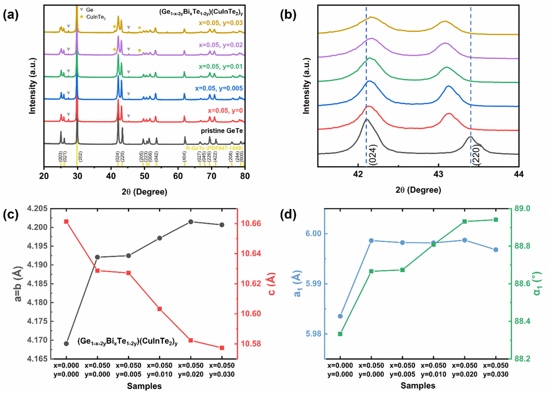 | ||
| Fig. 1 (a) XRD patterns of (Ge1−x−2yBixTe1−2y)(CuInTe2)y (x = 0 and 0.05; y = 0.005, 0.01, 0.02, and 0.03) samples. (b) Enlarged diffraction peaks of (024) and (220) in (a). (c) Experimental lattice parameters of (Ge1−x−2yBixTe1−2y)(CuInTe2)y. (d) The refined lattice parameter and interaxial angle based on a pseudo cubic unit cell. | ||
The calculated lattice parameters of (Ge1−x−2yBixTe1−2y)(CuInTe2)y increase along the a and b axes and decrease along the c axis, as shown in Fig. 1c and Table S1.† The lattice parameters of pristine GeTe (a = b = 4.169 Å and c = 10.661 Å) compared to those of (Ge0.89Bi0.05Te0.94)(CuInTe2)0.03 (a = b = 4.201 Å and c = 10.577 Å) are shown. This change can be attributed to the bigger ionic radius of Cu+ (0.96 Å), In3+ (0.81 Å), and Bi3+ (0.96 Å) in contrast to that of Ge2+ (0.73 Å). The expansion along the a and b axes and the contraction along the c axis of the rhombohedral structure imply a transition toward the cubic structure, which can also be confirmed with a refined lattice constant (a1) and interaxial angle (α1) based on a pseudo-cubic unit cell (Fig. 1d and Table S1†). After Bi doping, a1 and α1 increase simultaneously. With increasing y, a1 is maintained at ∼5.998 Å and α1 gradually increases and gets close to ∼89°. It is confirmed that the structural symmetry of alloyed GeTe is improved compared to that of the pristine sample.55,59 This increased structural symmetry from R3m to Fmm induces additional valence band convergence, contributing to the increase in the Seebeck coefficient,8,60 which will be discussed later.
The SEM image of the fracture surface of pristine GeTe is displayed in Fig. S1,† clearly showing a herringbone structure, which is a typical morphological characteristic of GeTe.61–63 Fig. S2† illustrates the SEM images and corresponding EDS mapping from the fracture surface. Fig. S2a† shows that the dark contrast phases in the SEM image are identified as Ge precipitates in the (Ge0.93Bi0.05Te0.98)(CuInTe2)0.01 sample. In Fig. S2b,† Cu and In are observed to be distributed in almost the same region in the (Ge0.89Bi0.05Te0.94)(CuInTe2)0.03 sample, and the CuInTe2 compound, which is also confirmed by XRD, is observed to be located around the grain boundary.
We performed quantitative analysis using EPMA to accurately verify the composition of the samples, and the results of point analysis are shown in Table 1. The EPMA results of the analyzed samples were reasonable compared to the nominal composition. In the matrices of (Ge0.93Bi0.05Te0.98)(CuInTe2)0.01 and (Ge0.89Bi0.05Te0.94)(CuInTe2)0.03, Cu and In not involved in the formation of CuInTe2 precipitates are evenly distributed. The results of the line scan between the matrix and precipitate at (Ge0.89Bi0.05Te0.94)(CuInTe2)0.03 are shown in Fig. S3.† The composition of the precipitate was ∼28.26 at% Cu, ∼21.92 at% In, and ∼42.77 at% Te, which was confirmed to be the CuInTe2 precipitate. This concurs well with the XRD results that CuInTe2 precipitates exist in the matrix. The small amount of Ge detected in the CuInTe2 precipitate is the Ge that is in the matrix beneath the CuInTe2 precipitate.
| Samples | Nominal composition (at%) | EPMA analyzed composition (at%) |
|---|---|---|
| Ge0.95Bi0.05Te | Ge47.5Bi2.5Te50 | Ge47.93Bi2.97Te49.10 |
| (Ge0.93Bi0.05Te0.98)(CuInTe2)0.01 | Ge46.5Bi2.5Cu0.5In0.5Te50 | Ge47Bi2.52Cu0.57In0.57Te49.34 |
| (Ge0.89Bi0.05Te0.94)(CuInTe2)0.03 | Ge44.5Bi2.5Cu1.5In1.5Te50 | Ge44.45Bi2.40Cu1.73In1.39Te50.04 |
To deeply understand the resulting microstructure of the (Ge0.93Bi0.05Te0.98)(CuInTe2)0.01 sample, we implemented field-emission transmission electron microscopy (FE-TEM). Fig. 2a shows a low-magnification bright-field TEM microscopy image, obviously exhibiting several herringbone structures composed of many domains and colonies.63 This structure is manifested by the disruption of Friedel's symmetry in the rhombohedral structure.63,64 The selected area electron diffraction (SAED) pattern along the [1![[1 with combining macron]](https://www.rsc.org/images/entities/char_0031_0304.gif)
![[2 with combining macron]](https://www.rsc.org/images/entities/char_0032_0304.gif) ] zone axis is shown in Fig. 2b, where there are split spots away from the transmitted beam (T), which are attributed to the neighbouring domains. The corresponding high-resolution TEM (HRTEM) micrograph in Fig. 2b identifies the interplanar distances as ∼0.21 nm and ∼0.35 nm, respectively, corresponding to the (220) and (11) planes. Fig. 2d indicates the occurrence of dislocations distributed through the inverse fast Fourier transformation (FFT) image in Fig. 2c. TEM-EDS analysis, depicted in Fig. S4,† revealed that Fig. 2e shows a GeTe matrix and dark-contrast CuInTe2 precipitates on the right. Fig. S5b† shows the contrast-adjusted image for accurate identification of the CuInTe2 precipitate. Fig. 2f shows the corresponding HRTEM micrograph of the red-square area in Fig. 2e, depicting the phase boundary between the GeTe matrix and CuInTe2 precipitate. The geometric phase analysis (GPA) is performed to investigate the strain distribution of the GeTe matrix and CuInTe2 precipitate.65,66 The CuInTe2 precipitate appears to be characterized by a relatively higher εxx (horizontal axis) and εyy (vertical axis) than the GeTe matrix, as shown in Fig. 2g and h. Such a nanoprecipitate with a difference in strain from the matrix, strong point defects, etc. interrupts the movement of phonons, which are the heat carriers, and contribute to the reduction of κlatt. In addition, as shown in Fig. 2i, the presence of CuInTe2 is confirmed once again in the SAED pattern showing the parallel crystal orientation relationship between the GeTe matrix and CuInTe2 precipitate. It can be observed that the reflected spots spread around the transmitted beam. This is due to the small difference in the lattice parameter between the GeTe matrix and CuInTe2 precipitate, which is illustrated with the schematic diagram in Fig. S6.†
] zone axis is shown in Fig. 2b, where there are split spots away from the transmitted beam (T), which are attributed to the neighbouring domains. The corresponding high-resolution TEM (HRTEM) micrograph in Fig. 2b identifies the interplanar distances as ∼0.21 nm and ∼0.35 nm, respectively, corresponding to the (220) and (11) planes. Fig. 2d indicates the occurrence of dislocations distributed through the inverse fast Fourier transformation (FFT) image in Fig. 2c. TEM-EDS analysis, depicted in Fig. S4,† revealed that Fig. 2e shows a GeTe matrix and dark-contrast CuInTe2 precipitates on the right. Fig. S5b† shows the contrast-adjusted image for accurate identification of the CuInTe2 precipitate. Fig. 2f shows the corresponding HRTEM micrograph of the red-square area in Fig. 2e, depicting the phase boundary between the GeTe matrix and CuInTe2 precipitate. The geometric phase analysis (GPA) is performed to investigate the strain distribution of the GeTe matrix and CuInTe2 precipitate.65,66 The CuInTe2 precipitate appears to be characterized by a relatively higher εxx (horizontal axis) and εyy (vertical axis) than the GeTe matrix, as shown in Fig. 2g and h. Such a nanoprecipitate with a difference in strain from the matrix, strong point defects, etc. interrupts the movement of phonons, which are the heat carriers, and contribute to the reduction of κlatt. In addition, as shown in Fig. 2i, the presence of CuInTe2 is confirmed once again in the SAED pattern showing the parallel crystal orientation relationship between the GeTe matrix and CuInTe2 precipitate. It can be observed that the reflected spots spread around the transmitted beam. This is due to the small difference in the lattice parameter between the GeTe matrix and CuInTe2 precipitate, which is illustrated with the schematic diagram in Fig. S6.†
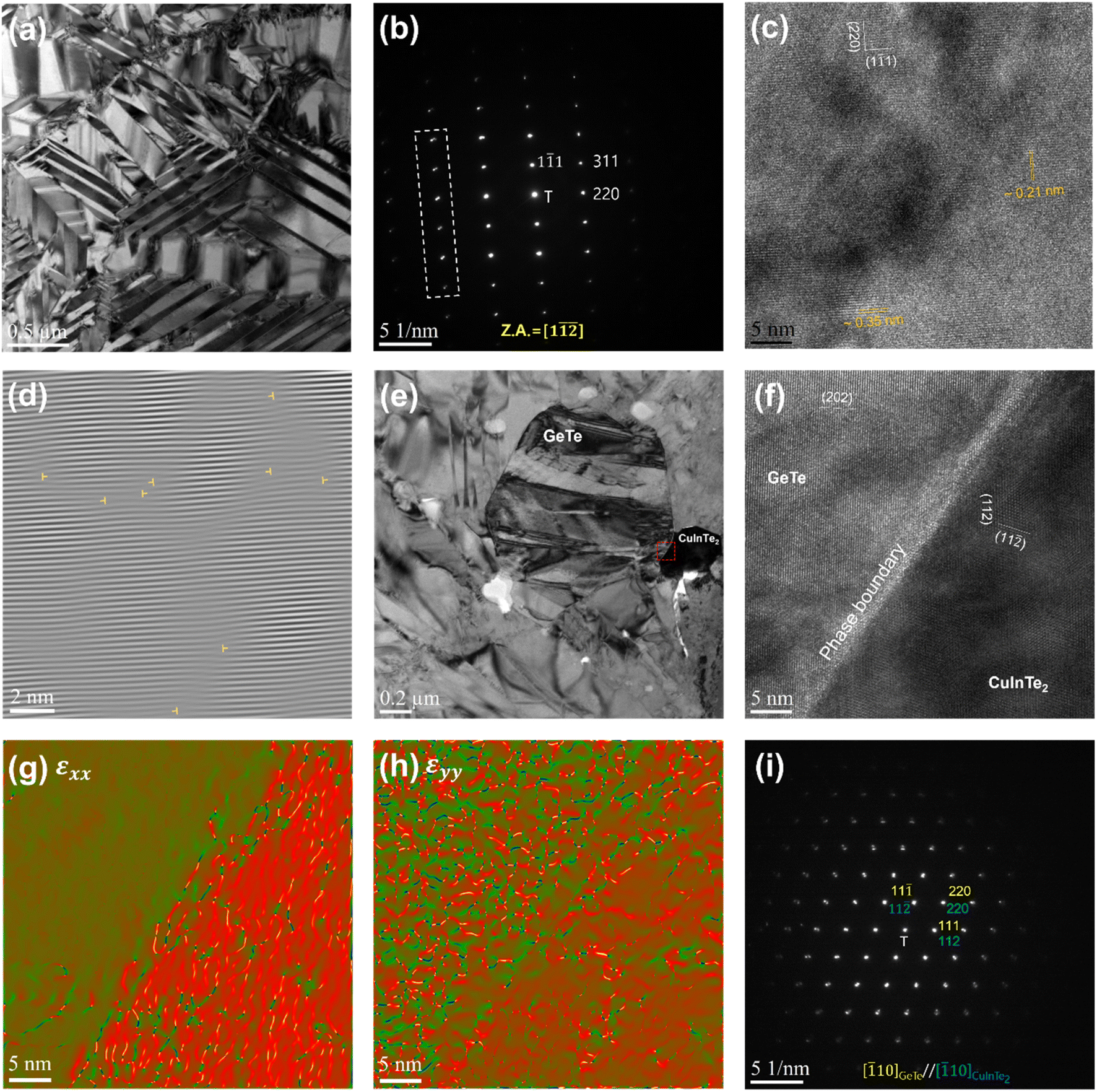 | ||
| Fig. 2 Microstructure observation in the (Ge0.93Bi0.05Te0.98)(CuInTe2)0.01 sample. (a) Bright-field TEM micrograph, showing the herringbone structures. (b) SAED pattern of rhombohedral GeTe along the [1] zone axis and the (c) corresponding HRTEM micrograph. (d) Inverse FFT image showing dislocations. (e) Bright-field TEM micrograph, showing a GeTe matrix grain and dark CuInTe2 precipitate. (f) HRTEM micrograph of the red-square area in (e). GPA mappings from (c) along the (g) horizontal (εxx) and (h) vertical (εyy) directions. (i) SAED pattern with GeTe and the CuInTe2 precipitate along the parallel zone axes. | ||
The electrical transport properties of (Ge1−x−2yBixTe1−2y)(CuInTe2)y samples are given in Fig. 3. Fig. 3a shows that the electrical conductivity generally decreases with increasing temperature, indicating the degenerated semiconductor behaviour. But for y is ≥0.01, the electrical conductivity increases slightly at ∼573 K. This is attributed to the valence band switch between L and Σ points induced by the second-order structural transition.34,48 In addition, this could be explained by an attenuated band bending at the interface between GeTe and CuInTe2, since the large Fermi level offset between the two materials at room temperature almost vanishes at around ∼600 K.67 The intrinsically high Ge vacancies in pristine GeTe contribute to having a high electrical conductivity value of 8400 S cm−1 at room temperature as shown in Fig. 3a. With the doping of 5% Bi, the electrical conductivity decreases to 2984 S cm−1, since Bi3+ effectively suppresses the Ge vacancies by providing an extra electron.34,57,58,68 Further alloying of CuInTe2 compounds, which have an intrinsically low carrier concentration (∼1018 cm−3),50 reduces the hole carrier concentration, leading to a gradual decrease in electrical conductivity at room temperature to 1953 S cm−1. Bi doping and CuInTe2 alloying can maintain the optimal carrier concentration (0.5–2.0 × 1020 cm−3) of GeTe-based materials from a doping content of y = 0.01, as depicted in Fig. 3d.69 In addition, Fig. 3e shows that GeTe compounds in this work have relatively higher mobility compared with those in previous reports.32,34,70–72 This can be elucidated by the reduced Ge vacancies and the similarity between the electronegativity of Ge and Cu.48,73
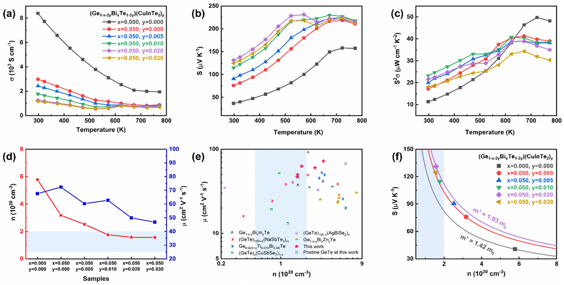 | ||
| Fig. 3 Temperature-dependent (a) electrical conductivity, (b) Seebeck coefficient, and (c) power factor of (Ge1−x−2yBixTe1−2y)(CuInTe2)y samples. (d) Composition-dependent Hall carrier concentration and Hall mobility at room temperature. Carrier concentration-dependent (e) Hall mobility in comparison with other reported data and (f) the Seebeck coefficient at room temperature. | ||
The Seebeck coefficient of (Ge1−x−2yBixTe1−2y)(CuInTe2)y samples is shown in Fig. 3b. The positive value of the Seebeck coefficient manifests a p-type semiconductor with holes acting as the majority charge carriers. The Seebeck coefficient is considerably enhanced after Bi doping and CuInTe2 alloying from ∼36.7 μV K−1 to ∼131 μV K−1 at room temperature. This is a result of the reduced carrier concentration (Fig. 3d) and the simultaneously increased effective mass (Fig. 3f). When the dopant composition is increased, the carrier concentration reaches an optimal level, and at the same time the effective mass increases due to changes in the electronic structure, including the hyperconvergence valence bands and the induced resonance level, as will be explained in the following section. The effective mass of (Ge1−x−2yBixTe1−2y)(CuInTe2)y samples is presented in the Pisarenko plot calculated with the single parabolic band (SPB) model. The effective mass increases from 1.42 m0 of pristine GeTe to 1.93 m0 of the (Ge0.91Bi0.05Te0.96)(CuInTe2)0.02 sample, where m0 is the electron mass. The temperature-dependent power factor is shown in Fig. 3c. Synergetically, an enhanced power factor of ∼23 μW cm−1 K−2 is obtained at room temperature and ∼41 μW cm−1 K−2 at 623 K in the (Ge0.93Bi0.05Te0.98)(CuInTe2)0.01 sample.
To better understand the improvement in the Seebeck coefficient of the multi-doped systems we compared the electronic structure of pristine GeTe with that of the multi-doped cubic system (Fig. 4a). We estimated a principal band gap of 0.26 eV at the Γ point in pristine GeTe due to the folding of the L point of the primitive cell Brillouin zone onto the Γ point of the supercell Brillouin zone.74 An energy gap of 0.20 eV and 0.19 eV was also observed between the light (at the Γ point) and heavy (at the Z + δ point in the Z → R direction) carrier sub-bands in the conduction and valence band regions, respectively, preventing the contribution of the heavy carrier bands towards the transport properties. A heavy hole band was also seen at the Γ + δ′ point in the Γ → X direction 0.06 eV below the valence band maximum. The partial density of states (pDOS) reveals that the valence band has a major contribution from the ‘p’ states of Te atoms and the conduction band, from the ‘p’ states of Ge atoms (Fig. 4b).
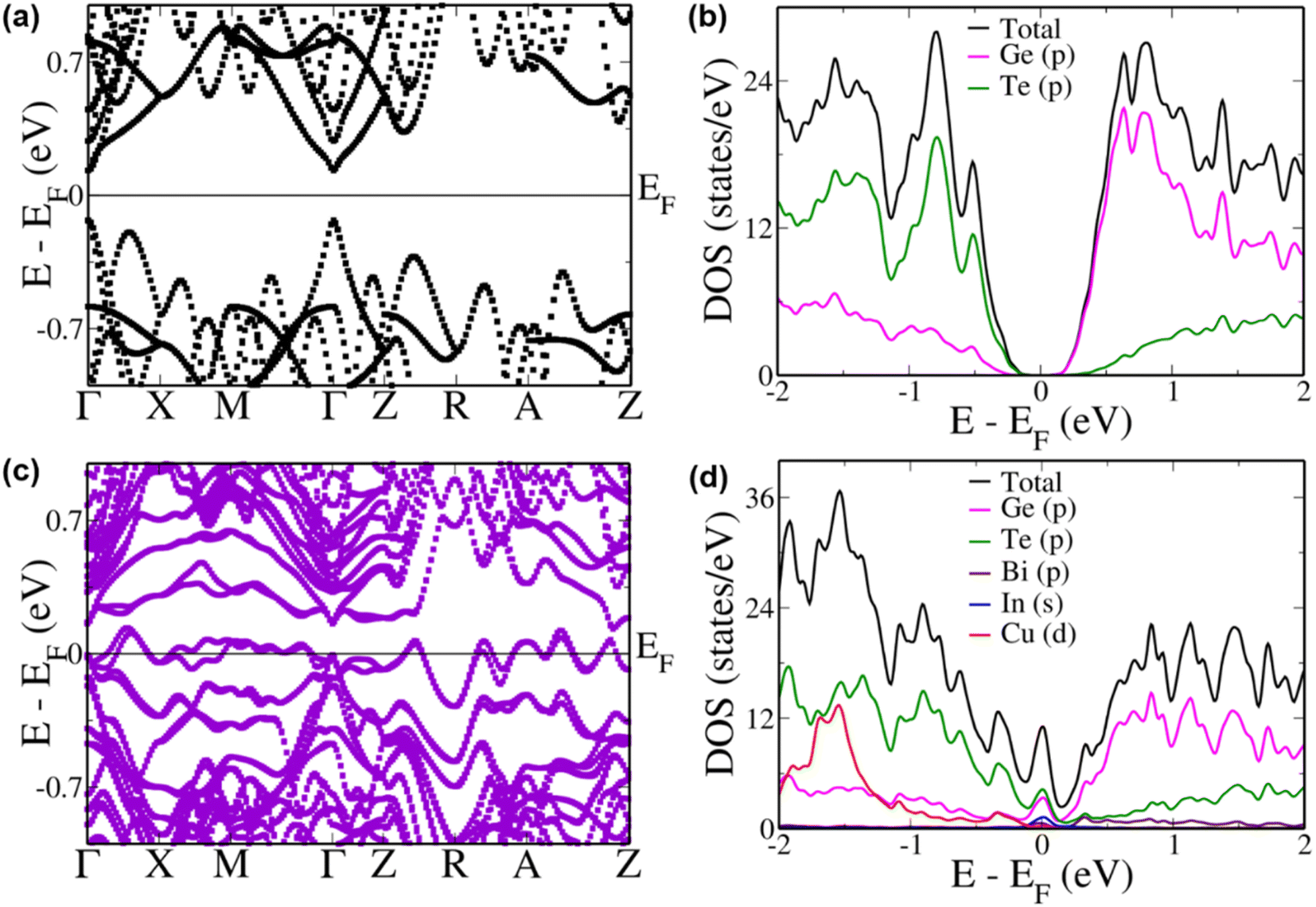 | ||
| Fig. 4 Electronic structure and pDOS of cubic (a and b) Ge16Te16; (c and d) Ge13BiInCuTe16. | ||
When Bi, In and Cu were doped simultaneously in GeTe we observe a very interesting electronic structure (Fig. 4c). Although we see a decrease in the energy gap at the Γ point by 0.1 eV in comparison to that of pristine GeTe, several favourable features appear near the Fermi level. The heavy hole sub-bands at the Z + δ point in the Z → R direction and the Γ + δ′ point in the Γ → X direction increase in energy to an energy higher than that of the light hole valence sub-band at the Γ point. Such a phenomenon of hyperconvergence of valence sub-bands in GeTe-based materials was observed previously only in the case of Zn doping.75 Even in the case of SnTe-based materials Zn was one of the dopants wherein such a feature of hyperconvergence of valence sub-bands was observed.76–78 This indicates that the current combination of dopants is very unique and is able to tune the electronic structure similar to a Zn dopant but with additional features. Such a feature of hyperconvergence along with the introduction of resonance states has previously been known to cause a drastic increase in the Seebeck coefficient even at lower temperatures aiding in an increase in the overall ZT of the material.76–78 The pDOS of this multi-doped GeTe composition shows a prominent increase in the DOS exactly at the Fermi level due to the hybridization of ‘s’ orbitals of In along with the ‘p’ orbitals of Ge and Te atoms (Fig. 4d). Unlike the case of In resonance levels in SnTe where the resonance states are formed by the hybridization of the resonant dopant atomic orbital with the orbital of the anion, here we see the involvement of the cation orbitals as well.79 This is further confirmed by analyzing the pDOS of In doped GeTe (Fig. S7†).
To study the contributions of individual dopants we analyzed the electronic structure of Bi, In and Cu doped GeTe separately (Fig. 5). In Bi doped GeTe, we see that the eight-fold degenerate conduction bands undergo splitting, and the lowermost doubly degenerate band touches the valence band maximum at the Γ point with 0.27 eV gap between the lowermost and the next set of conduction bands (Fig. 5a). The appearance of such resonance levels in GeTe due to Bi doping has been recently reported.37 The energy offset between the light and heavy carrier bands also decreases to 0.11 eV and 0.17 eV between the Γ and Z + δ points in the Z → R direction in the conduction and valence band regions. Similarly, when In is doped in GeTe, the eight-fold degenerate bands split with the uppermost doubly degenerate bands touching the conduction band minimum with an energy gap of 0.25 eV between the split bands at the Γ point (Fig. 5b). Here, we observe an energy offset of 0.21 eV and 0.04 eV between the light and heavy carrier sub-bands in the conduction and valence band regions. The presence of resonance levels is confirmed in the DOS plot in the form of a prominent hump near the Fermi level (Fig. 5d). Doping of Cu in GeTe, on the other hand, decreases the principal band gap to 0.18 eV, with an increase in the valence band energy offset between the Γ point and the Z + δ point in the Z → R direction and the Γ + δ′ point in the Γ → X direction to 0.25 eV and 0.07 eV (Fig. 5c). But it increases the energy of the bands at the M point leading to an energy difference of 0.17 eV from the valence band maximum at the Γ point compared to 0.45 eV in the case of pristine GeTe. Similarly, bands in the R → Z direction increase in energy with an energy difference of 0.15 eV between the A + δ′′ point in the A → Z direction and the valence band maximum at the Γ point. These features get more pronounced in the multi-doped GeTe, wherein the bands at the M point lie 0.08 eV above the valence band maximum at the Γ point and 0.162 eV at the A + δ′′ point in the A → Z direction revealing the impact of the right combination of dopants in aiding hyperconvergence. Similar features of the appearance of resonance levels and hyperconvergence of valence sub-bands are observed in the electronic structure and pDOS of the rhombohedral phase of multi-doped GeTe in comparison to that of pristine GeTe (Fig. S8†).
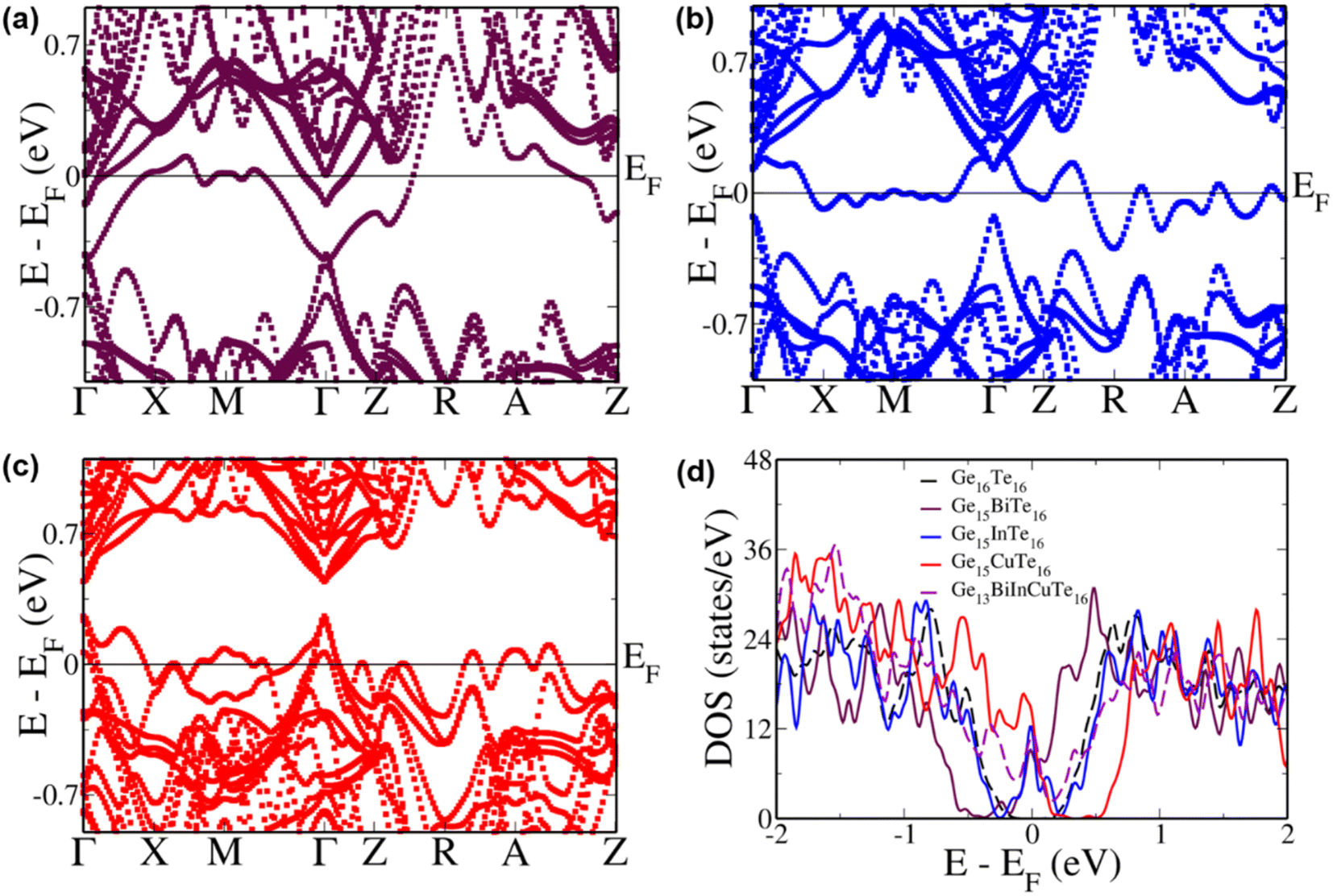 | ||
| Fig. 5 Electronic structure of cubic (a) Ge15BiTe16; (b) Ge15InTe16; (c) Ge15CuTe16; (d) Total DOS of undoped and doped configurations. | ||
Fig. 6a shows a plot of the temperature-dependent total thermal conductivity of (Ge1−x−2yBixTe1−2y)(CuInTe2)y (x = 0, 0.05; y = 0, 0.005, 0.01, 0.02, and 0.03) samples. The total thermal conductivity of pristine GeTe decreases with increasing temperature until 673 K. Above 673 K, the total thermal conductivity increases because pristine GeTe undergoes a ferroelectric phase transition, accompanying the structural relaxation along the <111> direction.34 With increasing x and y, the transition temperature decreases, indicating the expansion of the cubic structure region. Furthermore, the total thermal conductivity at room temperature significantly decreases from ∼7.36 W m−1 K−1 of pristine GeTe to ∼1.64 W m−1 K−1 of the (Ge0.91Bi0.05Te0.96)(CuInTe2)0.02 sample. This remarkable decrease is largely due to the decrease in electronic thermal conductivity (Fig. 6b) and partly due to the decrease in the lattice thermal conductivity (Fig. 6c). The reduction in electronic thermal conductivity is due to the reduced charge carrier concentration caused by the Bi doping and the CuInTe2 alloying, which result in lower electrical conductivity.
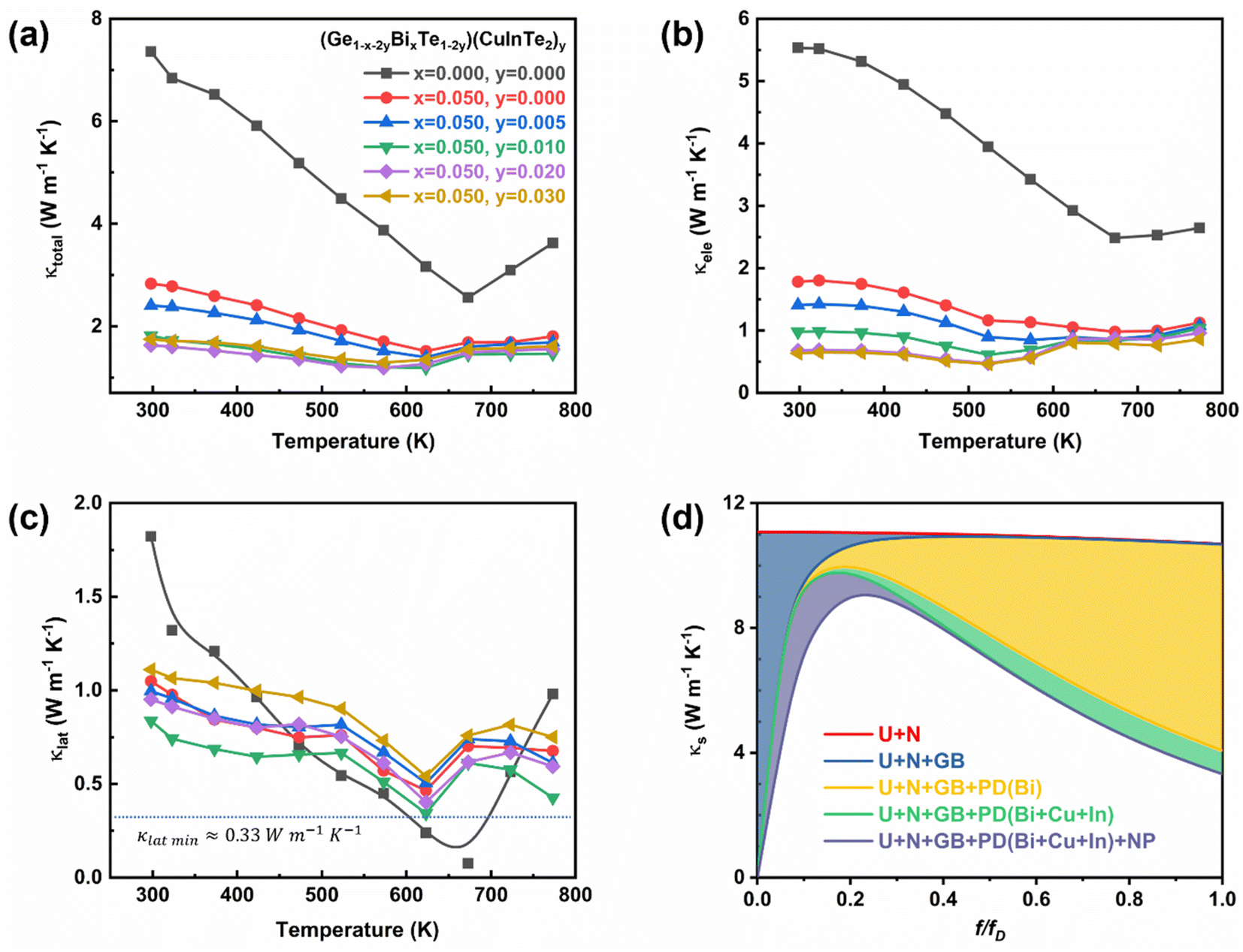 | ||
| Fig. 6 Temperature-dependent (a) total thermal conductivity, (b) electronic thermal conductivity, and (c) lattice thermal conductivity of (Ge1−x−2yBixTe1−2y)(CuInTe2)y samples. (d) Calculated spectral lattice thermal conductivity as a function of phonon frequency (f) based on various phonon scattering processes including the normal process (N), the Umklapp process (U), grain boundaries (GB), point defects (PD), and nanoprecipitate (NP) at 300 K. | ||
The lattice thermal conductivity reduces from ∼1.82 W m−1 K−1 of pristine GeTe to ∼0.84 W m−1 K−1 of the (Ge0.91Bi0.05Te0.96)(CuInTe2)0.02 sample. A minimum lattice thermal conductivity of ∼0.34 W m−1 K−1 is obtained at 623 K in the (Ge0.93Bi0.05Te0.98)(CuInTe2)0.01 sample, which is near the amorphous limit of ∼0.33 W m−1 K−1.80 This decline in lattice thermal conductivity is ascribed to increased phonon scattering induced by point defects and phase boundaries, as shown in Fig. 2f, between the matrix and CuInTe2 precipitate. Further insight is gained from the phonon frequency-dependent spectral lattice thermal conductivity shown in Fig. 6d calculated using the Debye–Callaway model,81–83 which includes scattering by intrinsic normal (N) and Umklapp (U) processes as well as extrinsic scattering by grain boundaries (GB), point defects (PD), and CuInTe2 nanoprecipitates (NP) after Bi doping and CuInTe2 alloying. The detailed methods and parameters are presented in the ESI.† The spectral lattice thermal conductivity decreases with increasing point defects introduced by the various dopants, especially at a high f/fD ratio, where f and fD are the phonon and Debye phonon frequency, respectively. However, the effect of nano-precipitates appears to be dominant at a low f/fD ratio and ineffective at a high f/fD ratio. Unfortunately, the lattice thermal conductivity gradually increases when the doping composition is increased in the (Ge0.91Bi0.05Te0.96)(CuInTe2)0.02 and (Ge0.89Bi0.05Te0.94)(CuInTe2)0.03 samples. This abnormal increase is due to the increased size and density of CuInTe2 precipitates (Fig. S2†) in the matrix and the difference in the κlatt between the precipitates and the host's matrix. The κlatt of CuInTe2 (∼6 W m−1 K−1) is significantly higher than that of the (Ge0.93Bi0.05Te0.98)(CuInTe2)0.01 sample.6,84,85
Consequently, the peak ZT value of ∼2.16 at 623 K is obtained in the (Ge0.93Bi0.05Te0.98)(CuInTe2)0.01 sample as depicted in Fig. 7a, due to the comprehensive contribution of the optimized carrier concentration, hyperconverged electronic structure, and all-scale hierarchical phonon scattering by Bi doping and CuInTe2 alloying. At room temperature, the ∼0.38 value of the (Ge0.93Bi0.05Te0.98)(CuInTe2)0.01 samples is almost 7 times higher than the ∼0.05 value of pristine GeTe. For practical applications as a thermoelectric device or module, a high average ZT (ZTavg) over the entire operating temperature range is also essential. The ZTavg is calculated by using ZTavg = Z{(Th + Tc)/2} and ranges from 300 K to 773 K.86 The obtained ZTavg value ∼1.42 of the (Ge0.93Bi0.05Te0.98)(CuInTe2)0.01 is significantly higher than those of previously reported Pb-free GeTe compounds, as shown in Fig. 7b.68,87–90 To more accurately predict the actual performance of a thermoelectric material at a given temperature difference, Fig. 7c and d indicate ZTeng and ηmax(ZTeng) calculated by the method proposed by Kim et al.86 for the (Ge1−x−2yBixTe1−2y)(CuInTe2)y (x = 0, 0.05; y = 0, 0.005, 0.01, 0.02, and 0.03) samples, which are dependent on a temperature difference (ΔT), and Tc is fixed as 300 K in the calculation. For the temperature difference ΔT = 473 K, the maximum ZTeng of the (Ge0.93Bi0.05Te0.98)(CuInTe2)0.01 sample is calculated to be ∼1.1, which is an increase of ∼250% and ∼50% compared to ∼0.31 for pristine GeTe and ∼0.73 for Ge0.95Bi0.05Te, respectively. Moreover, ηmax(ZTeng) is predicted to be as high as ∼15.4% in the (Ge0.93Bi0.05Te0.98)(CuInTe2)0.01 sample for the temperature difference ΔT = 473 K.
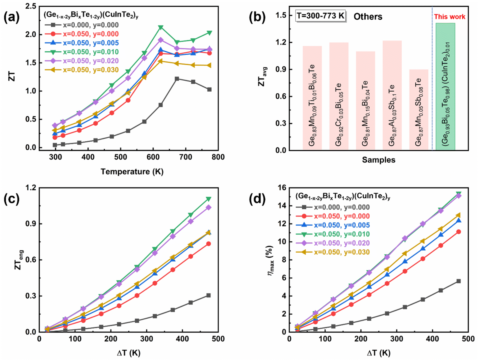 | ||
| Fig. 7 (a) Temperature-dependent ZT of (Ge1−x−2yBixTe1−2y)(CuInTe2)y samples and (b) the average ZT value with other reported GeTe compounds. (c) The ZTeng values and (d) ηmax values of (Ge1−x−2yBixTe1−2y)(CuInTe2)y samples. | ||
A thermoelectric material also requires sufficient mechanical stability. Vickers microhardness of the (Ge1−x−2yBixTe1−2y)(CuInTe2)y (x = 0, 0.05; y = 0, 0.005, 0.01, 0.02, and 0.03) samples was measured and is depicted in Fig. 8a. Pristine GeTe exhibits a value as low as ∼134 Hv, similar to that previously reported, due to the high concentration of Ge vacancies.8 Ge0.95Bi0.05Te and (Ge0.94Bi0.05Te0.99)(CuInTe2)0.005 exhibit values of ∼193 Hv and of ∼195 Hv, respectively, whereas (Ge0.93Bi0.05Te0.98)(CuInTe2)0.01, (Ge0.91Bi0.05Te0.96)(CuInTe2)0.02 and (Ge0.89Bi0.05Te0.91)(CuInTe2)0.03 achieve very high values of ∼230 Hv, ∼277 Hv, and ∼268 Hv, respectively. The improved mechanical strength is due to the dense point defects, the optimally reduced Ge vacancy concentration (Fig. 3d), and the strain induced by dislocations and CuInTe2 nanostructures (Fig. 2d, g, and h) with increasing dopant concentration. Fig. 8b shows the Hv values of our pristine GeTe and the (Ge0.91Bi0.05Te0.96)(CuInTe2)0.02 sample compared with the previously reported values of GeTe compounds,34,80,91,92 and it can be seen that the (Ge0.91Bi0.05Te0.96)(CuInTe2)0.02 sample value is super high.
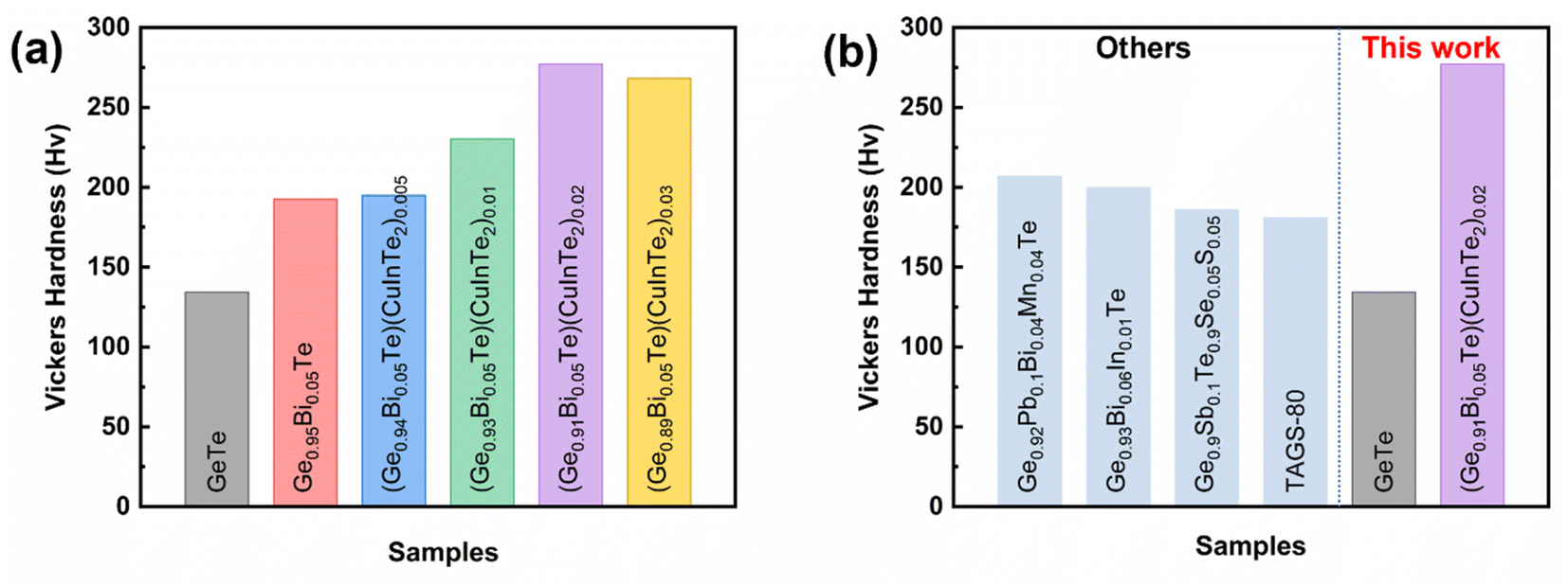 | ||
| Fig. 8 (a) Vickers hardness values of (Ge1−x−2yBixTe1−2y)(CuInTe2)y samples and (b) compared with those of other reported GeTe samples. | ||
Conclusions
In this study, the simultaneous addition of Bi and CuInTe2 to GeTe successfully adjusts the carrier concentration to an optimal level. The electronic structure calculations reveal the possibility of hyperconverged valence sub-bands and induced resonance levels. As the Seebeck coefficient increased, the power factor starts at ∼23 μW cm−1 K−2 at room temperature and peaks at 623 K with a value of ∼41 μW cm−1 K−2 in the (Ge0.93Bi0.05Te0.98)(CuInTe2)0.01 sample. The lattice thermal conductivity also decreased towards the amorphous limit. As a result, a peak ZT of ∼2.16 at 623 K and a ZTavg of ∼1.42 from 300 K to 773 K were obtained in the (Ge0.93Bi0.05Te0.98)(CuInTe2)0.01 sample. A record high Vickers hardness value of ∼277 Hv was obtained in the (Ge0.91Bi0.05Te0.96)(CuInTe2)0.02 sample.Conflicts of interest
The authors declare no conflicts of financial interest.Acknowledgements
This work was supported by grants from the National Research Foundation (NRF) of Korea (No. 2021R1A4A2001658 and 2022R1A2C1006790), and funded by the Korean government (MSIT). The author (USS) also acknowledges the grant from Science and Engineering Board, Department of Science and Technology, Government of India (SB/SRS/2021-22/73/CS) under the SERB Research Scientist scheme.References
- J. N. Kahiu, U. S. Shenoy, S. K. Kihoi, H. Kim, S. Yi, D. K. Bhat and H. S. Lee, J. Alloys Compd., 2022, 891, 162033 CrossRef CAS.
- M. Rakshit, D. Jana and D. Banerjee, J. Mater. Chem. A, 2022, 10, 6872–6926 RSC.
- Q. Wang, X. Xie, S. Li, Z. Zhang, X. Li, H. Yao, C. Chen, F. Cao, J. Sui, X. Liu and Q. Zhang, J. Materiomics, 2021, 7, 756–765 CrossRef.
- X. Yang, C. Wang, R. Lu, Y. Shen, H. Zhao, J. Li, R. Li, L. Zhang, H. Chen, T. Zhang and X. Zheng, Nano Energy, 2022, 101, 107553 CrossRef CAS.
- S. K. Kihoi, J. N. Kahiu, H. Kim, U. S. Shenoy, D. K. Bhat, S. Yi and H. S. Lee, J. Mater. Sci.: Mater. Electron., 2021, 85, 76–86 CAS.
- H. Kim, S. K. Kihoi and H. S. Lee, J. Alloys Compd., 2021, 869, 159381 CrossRef CAS.
- G. Tan, L. D. Zhao and M. G. Kanatzidis, Chem. Rev., 2016, 116, 12123–12149 CrossRef CAS PubMed.
- W. Di Liu, D. Z. Wang, Q. Liu, W. Zhou, Z. Shao and Z. G. Chen, Adv. Energy Mater., 2020, 10, 1–24 Search PubMed.
- L. E. Bell, Science, 2008, 321, 1457–1461 CrossRef CAS PubMed.
- X. Li, J. Liu, S. Li, J. Zhang, D. Li, R. Xu, Q. Zhang, X. Zhang, B. Xu, Y. Zhang, F. Xu and G. Tang, Nano Energy, 2020, 67, 104261 CrossRef CAS.
- Y. Pei, X. Shi, A. Lalonde, H. Wang, L. Chen and G. J. Snyder, Nature, 2011, 473, 66–69 CrossRef CAS PubMed.
- S. K. Kihoi, U. S. Shenoy, D. K. Bhat and H. S. Lee, J. Mater. Chem. C, 2021, 9, 9922–9931 RSC.
- J. P. Heremans, V. Jovovic, E. S. Toberer, A. Saramat, K. Kurosaki, A. Charoenphakdee, S. Yamanaka and G. J. Snyder, Science, 2008, 321, 1457–1461 CrossRef PubMed.
- B. Paul, A. Kumar V. and P. Banerji, J. Appl. Phys., 2010, 108, 064322 CrossRef.
- C. Gayner and Y. Amouyal, Adv. Funct. Mater., 2020, 30, 1–17 CrossRef.
- Y. L. Pei, H. Wu, D. Wu, F. Zheng and J. He, J. Am. Chem. Soc., 2014, 136, 13902–13908 CrossRef CAS PubMed.
- T. Berry, C. Fu, G. Auffermann, G. H. Fecher, W. Schnelle, F. Serrano-Sanchez, Y. Yue, H. Liang and C. Felser, Chem. Mater., 2017, 29, 7042–7048 CrossRef CAS.
- B. Jiang, Y. Yu, J. Cui, X. Liu, L. Xie, J. Liao, Q. Zhang, Y. Huang, S. Ning, B. Jia, B. Zhu, S. Bai, L. Chen, S. J. Pennycook and J. He, Science, 2021, 371, 830–834 CrossRef CAS PubMed.
- K. Biswas, J. He, I. D. Blum, C. I. Wu, T. P. Hogan, D. N. Seidman, V. P. Dravid and M. G. Kanatzidis, Nature, 2012, 489, 414–418 CrossRef CAS PubMed.
- Y. Luo, J. Yang, Q. Jiang, W. Li, Y. Xiao, L. Fu, D. Zhang, Z. Zhou and Y. Cheng, Nano Energy, 2015, 18, 37–46 CrossRef CAS.
- W. Li, Y. Luo, Y. Zheng, C. Du, Q. Liang, B. Zhu and L. Zhao, J. Mater. Sci. Technol., 2018, 29, 4732–4737 CAS.
- J. He, S. N. Girard, J. C. Zheng, L. Zhao, M. G. Kanatzidis and V. P. Dravid, Adv. Mater., 2012, 24, 4440–4444 CrossRef CAS PubMed.
- L. Hu, T. Zhu, X. Liu and X. Zhao, Adv. Funct. Mater., 2014, 24, 5211–5218 CrossRef CAS.
- Y. Yu, M. Cagnoni, O. Cojocaru-Mirédin and M. Wuttig, Adv. Funct. Mater., 2012, 24, 4440–4444 Search PubMed.
- N. Mingo, D. Hauser, N. P. Kobayashi, M. Plissonnier and A. Shakouri, Nano Lett., 2009, 9, 711–715 CrossRef CAS PubMed.
- T. Zhu, C. Fu, H. Xie, Y. Liu and X. Zhao, Adv. Energy Mater., 2015, 5, 1–13 Search PubMed.
- F. Gascoin, S. Ottensmann, D. Stark, S. M. Haïle and G. J. Snyder, Adv. Funct. Mater., 2005, 15, 1860–1864 CrossRef CAS.
- M. Rull-Bravo, A. Moure, J. F. Fernández and M. Martín-González, RSC Adv., 2015, 5, 41653–41667 RSC.
- S. Zhi, J. Li, L. Hu, J. Li, N. Li, H. Wu, F. Liu, C. Zhang, W. Ao, H. Xie, X. Zhao, S. J. Pennycook and T. Zhu, Adv. Sci., 2021, 8, 1–10 CrossRef PubMed.
- M. Hong, W. Lyv, M. Li, S. Xu, Q. Sun, J. Zou and Z. G. Chen, Joule, 2020, 4, 2030–2043 CrossRef CAS.
- Y. F. Tsai, M. Y. Ho, P. C. Wei and H. J. Wu, Acta Mater., 2022, 222, 117406 CrossRef CAS.
- S. Duan, W. Xue, H. Yao, X. Wang, C. Wang, S. Li, Z. Zhang, L. Yin, X. Bao, L. Huang, X. Wang, C. Chen, J. Sui, Y. Chen, J. Mao, F. Cao, Y. Wang and Q. Zhang, Adv. Energy Mater., 2022, 12, 1–8 Search PubMed.
- M. Li, Q. Sun, S. D. Xu, M. Hong, W. Y. Lyu, J. X. Liu, Y. Wang, M. Dargusch, J. Zou and Z. G. Chen, Adv. Mater., 2021, 33, 1–8 Search PubMed.
- S. Perumal, M. Samanta, T. Ghosh, U. S. Shenoy, A. K. Bohra, S. Bhattacharya, A. Singh, U. V. Waghmare and K. Biswas, Joule, 2019, 3, 2565–2580 CrossRef CAS.
- J. P. Gaspard, C. R. Phys., 2016, 17, 389–405 CrossRef CAS.
- J. Li, X. Zhang, Z. Chen, S. Lin, W. Li, J. Shen, I. T. Witting, A. Faghaninia, Y. Chen, A. Jain, L. Chen, G. J. Snyder and Y. Pei, Joule, 2018, 2, 976–987 CrossRef CAS.
- U. S. Shenoy, K. D. Goutham and D. K. Bhat, J. Alloys Compd., 2022, 921, 165965 CrossRef CAS.
- A. Manchon, H. C. Koo, J. Nitta, S. M. Frolov and R. A. Duine, Nat. Mater., 2015, 14, 871–882 CrossRef CAS PubMed.
- T. Xing, C. Zhu, Q. Song, H. Huang, J. Xiao, D. Ren, M. Shi, P. Qiu, X. Shi, F. Xu and L. Chen, Adv. Mater., 2021, 2008773 CrossRef CAS PubMed.
- X. Wang, W. Xue, Z. Zhang, X. Li, L. Yin, C. Chen, B. Yu, J. Sui, F. Cao, X. Liu, J. Mao, Y. Wang, X. Lin and Q. Zhang, ACS Appl. Mater. Interfaces, 2021, 13, 45717–45725 CrossRef CAS PubMed.
- K. S. Bayikadi, C. T. Wu, L. C. Chen, K. H. Chen, F. C. Chou and R. Sankar, J. Mater. Chem. A, 2020, 8, 5332–5341 RSC.
- L. Wu, X. Li, S. Wang, T. Zhang, J. Yang, W. Zhang, L. Chen and J. Yang, NPG Asia Mater., 2017, 9, 1–7 Search PubMed.
- Y. Jin, Y. Xiao, D. Wang, Z. Huang, Y. Qiu and L. D. Zhao, ACS Appl. Energy Mater., 2019, 2, 7594–7601 CrossRef CAS.
- M. Hong, Y. Wang, T. Feng, Q. Sun, S. Xu, S. Matsumura, S. T. Pantelides, J. Zou and Z. G. Chen, J. Am. Chem. Soc., 2019, 141, 1742–1748 CrossRef CAS PubMed.
- B. Jiang, W. Wang, S. Liu, Y. Wang, C. Wang, Y. Chen, L. Xie, M. Huang and J. He, Science, 2022, 377, 208–213 CrossRef CAS PubMed.
- S. H. Yang, T. J. Zhu, T. Sun, J. He, S. N. Zhang and X. B. Zhao, Nanotechnology, 2008, 19, 245707 CrossRef CAS PubMed.
- N. Li, W. He, C. Li, G. Wang, G. Wang, X. Zhou and X. Lu, J. Mater. Chem. A, 2021, 9, 2385–2393 RSC.
- Q. Zhang, Z. Ti, Y. Zhu, Y. Zhang, Y. Cao, S. Li, M. Wang, D. Li, B. Zou, Y. Hou, P. Wang and G. Tang, ACS Nano, 2021, 15, 19345–19356 CrossRef CAS PubMed.
- H. Kim, C. O. Park, H. Jeong, S. K. Kihoi, S. Yi, H. S. Kim, K. H. Lee and H. S. Lee, Inorg. Chem. Front., 2021, 8, 2782–2787 RSC.
- Y. Luo, J. Yang, Q. Jiang, W. Li, D. Zhang, Z. Zhou, Y. Cheng, Y. Ren and X. He, Adv. Energy Mater., 2016, 6, 1600007 CrossRef.
- A. Kosuga, K. Umekage, M. Matsuzawa, Y. Sakamoto and I. Yamada, Inorg. Chem., 2014, 53, 6844–6849 CrossRef CAS PubMed.
- H. S. Kim, Z. M. Gibbs, Y. Tang, H. Wang and G. J. Snyder, APL Mater., 2015, 3, 1–6 Search PubMed.
- P. Giannozzi, S. Baroni, N. Bonini, M. Calandra, R. Car, C. Cavazzoni, D. Ceresoli, G. L. Chiarotti, M. Cococcioni, I. Dabo, A. Dal Corso, S. De Gironcoli, S. Fabris, G. Fratesi, R. Gebauer, U. Gerstmann, C. Gougoussis, A. Kokalj, M. Lazzeri, L. Martin-Samos, N. Marzari, F. Mauri, R. Mazzarello, S. Paolini, A. Pasquarello, L. Paulatto, C. Sbraccia, S. Scandolo, G. Sclauzero, A. P. Seitsonen, A. Smogunov, P. Umari and R. M. Wentzcovitch, J. Phys.: Condens. Matter, 2009, 21, 395502 CrossRef PubMed.
- J. P. Perdew, K. Burke and M. Ernzerhof, Phys. Rev. Lett., 1996, 77, 3865–3868 CrossRef CAS PubMed.
- R. Zhang, J. Pei, Z. Shan, W. Zhou, Y. Wu, Z. Han, Y. H. Zhao, J. F. Li, Z. H. Ge and B. P. Zhang, Chem. Eng. J., 2022, 429, 132275 CrossRef CAS.
- J. Li, Z. Chen, X. Zhang, H. Yu, Z. Wu, H. Xie, Y. Chen and Y. Pei, Adv. Sci., 2017, 4, 1700341 CrossRef PubMed.
- H. Jeong, S. K. Kihoi, H. Kim and H. S. Lee, J. Mater. Res. Technol., 2021, 15, 6312–6318 CrossRef CAS.
- S. Perumal, P. Bellare, U. S. Shenoy, U. V. Waghmare and K. Biswas, Chem. Mater., 2017, 29, 10426–10435 CrossRef CAS.
- C. Zhu, J. Wang, F. Luo, S. Zhang, J. Wang, Y. Zhang, H. Liu and Z. Sun, ACS Appl. Mater. Interfaces, 2022, 14, 38854–38864 CrossRef CAS PubMed.
- S. Perumal, S. Roychowdhury, D. S. Negi, R. Datta and K. Biswas, Chem. Mater., 2015, 27, 7171–7178 CrossRef CAS.
- A. S. Frolov, J. Sánchez-Barriga, C. Callaert, J. Hadermann, A. V. Fedorov, D. Y. Usachov, A. N. Chaika, B. C. Walls, K. Zhussupbekov, I. V. Shvets, M. Muntwiler, M. Amati, L. Gregoratti, A. Y. Varykhalov, O. Rader and L. V. Yashina, ACS Nano, 2020, 14, 16576–16589 CrossRef CAS PubMed.
- M. Snykers, P. Delavignette and S. Amelinckx, Mater. Res. Bull., 1972, 7, 831–839 CrossRef CAS.
- H. S. Lee, B. S. Kim, C. W. Cho, M. W. Oh, B. K. Min, S. D. Park and H. W. Lee, Acta Mater., 2015, 91, 83–90 CrossRef CAS.
- D. Wu, L. D. Zhao, S. Hao, Q. Jiang, F. Zheng, J. W. Doak, H. Wu, H. Chi, Y. Gelbstein, C. Uher, C. Wolverton, M. Kanatzidis and J. He, J. Am. Chem. Soc., 2014, 136, 11412–11419 CrossRef CAS PubMed.
- H. Wu, F. Zheng, D. Wu, Z. H. Ge, X. Liu and J. He, Nano Energy, 2015, 13, 626–650 CrossRef CAS.
- M. J. Hÿtch, E. Snoeck and R. Kilaas, Ultramicroscopy, 1998, 74, 131–146 CrossRef.
- S. Hui, W. Gao, X. Lu, A. Panda, T. P. Bailey, A. A. Page, S. R. Forrest, D. T. Morelli, X. Pan, K. P. Pipe and C. Uher, Adv. Energy Mater., 2018, 8, 1–8 Search PubMed.
- Z. Liu, J. Sun, J. Mao, H. Zhu, W. Ren, J. Zhou, Z. Wang, D. J. Singh, J. Sui, C. W. Chu and Z. Ren, Proc. Natl. Acad. Sci. U. S. A., 2018, 115, 5332–5337 CrossRef CAS PubMed.
- Z. Bu, W. Li, J. Li, X. Zhang, J. Mao, Y. Chen and Y. Pei, Mater. Today Phys., 2019, 9, 1–7 Search PubMed.
- C. Zhu, F. Luo, J. Wang, S. Zhang, J. Wang, H. Liu and Z. Sun, J. Mater. Chem. C, 2022, 14, 9052–9061 RSC.
- N. Man, J. Cai, Z. Guo, G. Liu, P. Sun, H. Wang, Q. Zhang, X. Tan, Y. Yin and J. Jiang, ACS Appl. Energy Mater., 2021, 4, 4242–4247 CrossRef CAS.
- M. Samanta, T. Ghosh, R. Arora, U. V. Waghmare and K. Biswas, J. Am. Chem. Soc., 2019, 141, 19505–19512 CrossRef CAS PubMed.
- L. C. Yin, W. Di Liu, M. Li, Q. Sun, H. Gao, D. Z. Wang, H. Wu, Y. F. Wang, X. L. Shi, Q. Liu and Z. G. Chen, Adv. Energy Mater., 2021, 11, 1–8 Search PubMed.
- D. K. Bhat and U. S. Shenoy, J. Alloys Compd., 2020, 843, 155989 CrossRef CAS.
- D. K. Bhat and U. S. Shenoy, New J. Chem., 2020, 44, 17664–17670 RSC.
- U. S. Shenoy and D. K. Bhat, J. Mater. Chem. C, 2020, 8, 2036–2042 RSC.
- D. K. Bhat and U. S. Shenoy, J. Alloys Compd., 2020, 834, 155181 CrossRef CAS.
- U. S. Shenoy and D. K. Bhat, J. Alloys Compd., 2022, 892, 162221 CrossRef CAS.
- U. S. Shenoy and D. K. Bhat, J. Mater. Chem. C, 2019, 7, 4817–4821 RSC.
- D. Z. Wang, W. Di Liu, M. Li, L. C. Yin, H. Gao, Q. Sun, H. Wu, Y. Wang, X. L. Shi, X. Yang, Q. Liu and Z. G. Chen, Chem. Eng. J., 2022, 441, 136131 CrossRef CAS.
- J. Callaway and H. C. Von Baeyer, Phys. Rev., 1960, 120, 1149–1154 CrossRef CAS.
- D. Bessas, I. Sergueev, H. C. Wille, J. Peron, D. Ebling and R. P. Hermann, Phys. Rev. B: Condens. Matter Mater. Phys., 2012, 86, 1–9 CrossRef.
- M. Hong, T. C. Chasapis, Z. G. Chen, L. Yang, M. G. Kanatzidis, G. J. Snyder and J. Zou, ACS Nano, 2016, 10, 4719–4727 CrossRef CAS PubMed.
- Y. M. Zhou, H. J. Wu, Y. L. Pei, C. Chang, Y. Xiao, X. Zhang, S. K. Gong, J. Q. He and L. D. Zhao, Acta Mater., 2017, 125, 542–549 CrossRef CAS.
- X. L. Shi, J. Zou and Z. G. Chen, Chem. Rev., 2020, 120, 7399–7515 CrossRef CAS PubMed.
- H. S. Kim, W. Liu, G. Chen, C. W. Chu and Z. Ren, Proc. Natl. Acad. Sci. U. S. A., 2015, 112, 8205–8210 CrossRef CAS PubMed.
- A. Kumar, P. Bhumla, T. Parashchuk, S. Baran, S. Bhattacharya and K. T. Wojciechowski, Chem. Mater., 2021, 33, 3611–3620 CrossRef CAS.
- C. Xu, Z. Liang, W. Ren, S. Song, F. Zhang and Z. Ren, Adv. Energy Mater., 2022, 12, 2202392 CrossRef CAS.
- Y. Dou, J. Li, Y. Xie, X. Wu, L. Hu, F. Liu, W. Ao, Y. Liu and C. Zhang, Mater. Today Phys., 2021, 20, 100497 CrossRef CAS.
- J. Shuai, Y. Sun, X. Tan and T. Mori, Small, 2020, 16, 1906921 CrossRef CAS PubMed.
- M. Samanta and K. Biswas, J. Am. Chem. Soc., 2017, 139, 9382–9391 CrossRef CAS PubMed.
- J. Davidow and Y. Gelbstein, J. Electron. Mater., 2013, 42, 1542–1549 CrossRef CAS.
Footnote |
| † Electronic supplementary information (ESI) available. See DOI: https://doi.org/10.1039/d2ta09280h |
| This journal is © The Royal Society of Chemistry 2023 |