
 Open Access Article
 This Open Access Article is licensed under a Creative Commons Attribution-Non Commercial 3.0 Unported Licence
A novel N-doped carbon nanomaterial – carbon nano-mousse†
Michal
Lesňák
a,
Daniel
Cvejn
 *b,
Martin
Petr
c,
Pavlína
Peikertová
a,
Roman
Gabor
a,
Tibor
Fördös
ad,
Pavel
Czernek
a and
Daniela
Plachá
ab
*b,
Martin
Petr
c,
Pavlína
Peikertová
a,
Roman
Gabor
a,
Tibor
Fördös
ad,
Pavel
Czernek
a and
Daniela
Plachá
ab
aNanotechnology Centre, CEET, VSB – Technical University of Ostrava, 17. Listopadu 2172/15, 708 00 Ostrava-Poruba, Czech Republic
bENET Centre, CEET, VSB – Technical University of Ostrava, 17. Listopadu 2172/15, 708 00 Ostrava-Poruba, Czech Republic. E-mail: daniel.cvejn@vsb.cz
cRegional Centre of Advanced Technologies and Materials, Czech Advanced Technology and Research Institute, Palacký University, Šlechtitelů 27, 783 71 Olomouc, Czech Republic
dIT4Innovations, VSB – Technical University of Ostrava, 17. Listopadu 2172/15, 708 00 Ostrava-Poruba, Czech Republic
First published on 9th February 2023
Abstract
A novel N-doped carbon material was obtained using a CVD-like procedure by depositing medium-sized pyridine-based molecules on copper-based substrates. The resulting material is a system of interconnected multi-wall carbon nanospheres (approx. 200 nm in diameter) with substantial N-doping (up to 14.8 atom% according to XPS). This material was named “nano-mousse” as it resembles the mousse on champagne in the electron microscopy images. A series of N-doped carbon nano-mousses were prepared by varying the temperature and precursor of the procedure. All of the nano-mousses were characterized by XPS and Raman microspectroscopy. Selected samples were further studied by several types of electron microscopies and spectroscopic ellipsometry. As it appears, N-doped carbon nano-mousses have metal-like properties in terms of optical conductivity and other optical properties, along with macroscopic appearance. XPS and Raman microspectroscopy revealed that their structure and chemical composition is highly dependent on both the nature of the precursor and preparation conditions.
1. Introduction
Nitrogen-doped (N-doped) carbon nanostructures, whether 0D (fullerenes1 and quantum dots2), 1D (nanotubes3–5), 2D (graphene mono-layers6,7 or oligo-layers8–10) or 3D (nano-foams11 and diamond-like carbons12), have been finding use in multiple modern applications, including supercapacitors,8,13 batteries,14,15 fuel cells,16 semiconductor-technologies,2 photocatalysis,17 and photonics.18 Some of these materials are currently being commercialized or are on the verge of being commercialized.19 While being promising materials in all of the aforementioned fields, their use beyond experimental devices is still limited.20,21 The principal reason for this is the complicated reproducibility of their syntheses in terms of the texture and structure (type of carbon lattice and type of N-enrichment) of the desired material. Few reproducible protocols of their syntheses are found more or less empirically and are highly sensitive to both internal (type of precursor) and external (pressure, temperature, and atmosphere of synthesis) conditions.The vast majority of known N-doped carbon materials are prepared from some sort of precursors by applying a source of high energy either (solvo)thermal,22 electric,23 or even mechanical (e.g., ball milling8). Precursors can be sorted into C-sources (sourcing carbon to the final structure primarily), N-sources (bringing nitrogen into the final structure primarily), or C, N-sources (bringing both). The C, N-sources, as well as the C-sources and N-sources, can be further sorted into small molecules (Mw < 150, usually basic cheap chemicals containing carbon and/or nitrogen such as methylamine,6 nitromethane, aniline,24 and pyridine25), polymeric materials (Mw >> 1000; C, N-containing polymers such as polypyrrole,15,26 polyaniline,27 and polyurethane28) or biomaterials, including, bio-waste.29 Chemical composition of carbon materials prepared from small molecular precursors (C, N-sources or a combination of such C-sources and N-sources) is usually controllable merely by physical conditions of preparation (temperature, gas phase pressure, etc.).30 Polymers can direct the chemical nature of N-doping in the final structure, yet they are not very versatile precursors, and they usually have to be pre-made, making them less affordable starting materials. Bio-materials, especially bio-waste, are quite inexpensive and usually environmentally friendly starting materials, offering some control over the structure of the final material.31 On the other hand, they are inherently heterogeneous both in the sense of one batch (intrinsic heterogeneity) and in the sense of different batches and syntheses thereof suffer from low reproducibility and reliability.
Apart from the texture (0D, 1D, 2D or 3D materials with their subclasses, vide supra), the key element of the properties of N-doped carbon nanostructures is the type of N-enrichment.32 There are three major types of this doping that are consistently observed in carbon materials – pyridinic nitrogen, pyrrolic nitrogen, and quaternary/graphitic nitrogen.33 Each of them has very different impacts on the electronic structure of the material and, therefore, its properties.34 One way to make the preparation of N-doped materials more effective is to improve the control of particular N-enrichment or better control of their mix.33
With this in mind, we hypothesized that medium-sized N-containing molecules (Mw > 150; Mw < 1000) can provide a restricted number of degrees of freedom in the construction of N-doped carbon materials and, therefore, when treated with a high energy process, can yield an N-doped material with partial control of a particular type of N-enrichment. We anticipated that more complex structures would produce a mix of radicals, which can dramatically influence the reaction chemistry while still being relatively small molecules that can easily transfer to the gas state.
Thus, we decided to test this hypothesis on a series of three pyridine-based precursors N-(pyridin-4-yl)pyridine-4-amine (1), 4,4′-diazene-1,2-diyldipyridine (2) and N,N′,N′′-tris(pyridin-4-yl)-1,3,5-triazine-2,4,6-triamine (3) as their polymerization/carbonization in temperatures over 500 °C was likely to direct a particular type of N-enrichment. A thermal exposition of 1 should, in our hypotheses, lead to pyridinic and pyrrolic nitrogen, 2 should preferably be a source of pyridine nitrogen, while 3 could also introduce quaternary nitrogen to the structure (Fig. 1). An apparatus of CVD preparations (see Methods, Section 4.3) appeared as the most suitable experimental setup for testing these hypotheses.
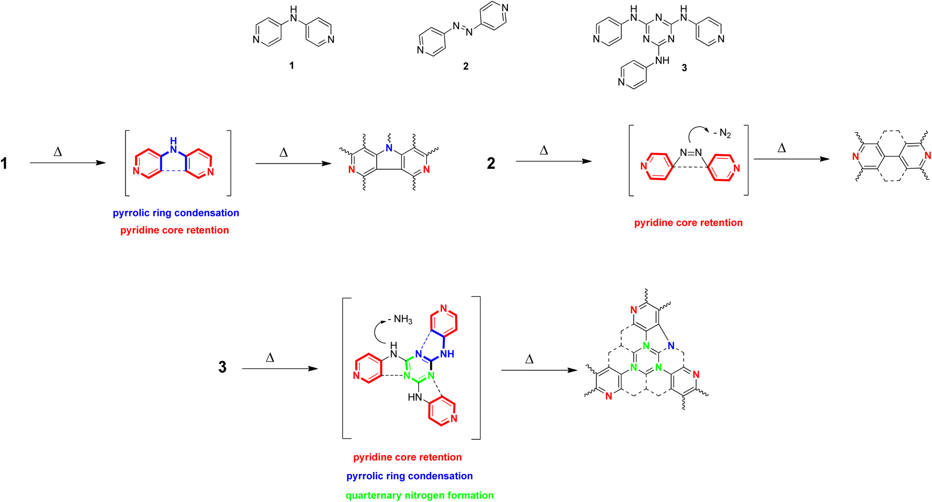 | ||
| Fig. 1 Selected precursors 1, 2 and 3 and our hypothetical proposal of their hypothetical influence on the final structure. 1 is proposed to form pyridinic and pyrrolic nitrogen rich carbon materials, 2 should form exclusively pyridinic nitrogen rich carbon materials, 3 can be a source of pyridinic, pyrrolic and graphitic nitrogens in a carbon structure. | ||
With that in mind, we hypothesized that medium sized N-containing molecules (Mw > 150; Mw < 1000) can provide restricted number of degrees of freedom in the construction of N-doped carbon materials and, therefore, when treated with a high energy process, can yield an N-doped material with a partial control of a particular type of N-enrichment. We decided to test this hypothesis on a series of three pyridine-based precursors N-(pyridin-4-yl)pyridine-4-amine (1), 4,4′-diazene-1,2-diyldipyridine (2) and N,N′,N′′-tris(pyridin-4-yl)-1,3,5-triazine-2,4,6-triamine (3) as their polymerization/carbonization in temperatures over 500 °C was likely to direct a particular type of N-enrichment. A thermal exposition of 1 should in our hypotheses lead to pyridinic and pyrrolic nitrogen, 2 should be preferably a source of pyridine nitrogen, while 3 could introduce also quaternary nitrogen to the structure (Fig. 1). An apparatus of CVD preparations (see Methods, Section 4.3) appeared as the most suitable experimental setup for testing these hypotheses.
The aim of this work was to describe the results of those experiments along with chemical and physical characterizations of gained materials.
2. Results and discussion
2.1. Sample denomination and experimental setup
Carbonic layers were prepared on copper sheets as substrates from precursors 1, 2, and 3 at temperatures 1050 °C, 900 °C, 750 °C, 600 °C, and 500 °C. For clarity, particular samples were denoted as X-TTT, where X is the original precursor (1, 2 or 3) and TTT is the temperature (in °C) of its preparation. Therefore, for example, sample 1-900 is the sample made from precursor 1 at 900 °C. Ten prepared samples (1-1050, 1-900, 1-750, 2-1050, 2-900, 2-750, 2-600, 2-500, 3-1050, and 3-900) provided a layer of the same type of material described in this publication. At temperatures lower than 750 °C, 500 °C, and 900 °C for materials 1, 2, and 3, respectively, nothing other than an amorphous carbon was detected as a product; thus, the results are not shown. The aforementioned samples, on the other hand, were uniformly colored with a greyish-metallic tinge (Fig. 2), which covered the entire copper surface of the original sheets. For better feasibility of different spectroscopic analyses, parallel samples using alternative copper-based substrates were also made. Samples denoted X-TTTa were samples in which copper TEM targets (without any surface coating) were used as substrates to enable direct STEM characterization of materials without any further modifications. Samples denoted X-TTTb were samples in which silicon wafers were coated with 200 nm of copper by physical vapor deposition (PVD)35 to enable enhanced SEM measurements and ellipsometry measurements. Parallel samples X-TTT, X-TTTa, and X-TTTb were otherwise made under the same conditions differing only with the particular copper-based substrates, and as far as it could be observed, each particular sample X-TTT/X-TTTa/X-TTTb has the same properties. | ||
| Fig. 2 Chosen photography of the sample 1-750 carbon layer on copper sheet is a representative of the appearance of most of the samples. | ||
The greyish-metallic colored X-TTT materials were formed on the copper substrate only. The weight difference of a copper slice (substrate) before the procedure and after was, on average, 0.26 mg when 30 mg of the precursor was used, therefore yielding 0.9% of the mass of the original precursor. It should be, though, noted that precursor yield is highly dependent on the accessible copper surface, which has been intentionally reduced in order to create an experimentally friendly setup and easier analysis of materials. Maximum yields might be significantly higher. The rest of the test tube (see Methods, Section 4.3) as also covered with a material of carbonic nature. On the cooler parts of the CVD-apparatus, the material precursors 1, 2, and 3 desublimated, forming their initial state usually only with a trace of heat-generated impurities (e.g. 4,4′-bipyridine in the case of 2, detected by GC/MS, see Methods, Section 4.1). This fact suggests that the classical CVD process, in fact, did not take place, as the CVD process presumes decomposition of precursor to plasma/ionized gas state and, therefore, desublimation should not occur. That is why the preparation is in this text referred to as CVD-like preparation.
2.2. Texture and structure of gained materials
The texture and structure of gained samples have been studied by AFM, SEM, STEM, and HR-TEM (Fig. 3 and 4), EDX spectroscopy, Raman microspectrometry, and X-ray photoelectron spectroscopy (XPS). Several attempts were made to record XRD patterns and electron diffraction (as a part of HR-TEM instrumentation), yet the material, though clearly having a repetitive structure, failed to yield an interpretable diffraction pattern. Microscopies (Fig. 3 and 4) have proven the characteristics of the gained material. Carbon particles are visibly organized in spherical units of diameters between 200 and 400 nm (median around 250 nm), which are chained into tubular structures intertwined into a bulk material. According to AFM microscopy (see ESI Fig. S42 to S44†), the thickness of the material on a copper substrate is uniformly around 100 nm. EDS images (from SEM, STEM, and HR-TEM) of randomly selected areas indicated the presence of carbon throughout all of the samples. Nitrogen and oxygen were spotted mainly in 1-1050 by this methodology. A better insight has been made by EDX mapping of samples 1-1050b and 2-750b (Fig. 4). Yet, EDS was not deemed as a source reliable enough for the determination of elemental compositions. Therefore, the elemental composition was further characterized by XPS (vide infra). The majority of the microscopic images show that carbon layers form a texture resembling the texture of mousse on champagne. That is why we named the material as nano-mousse.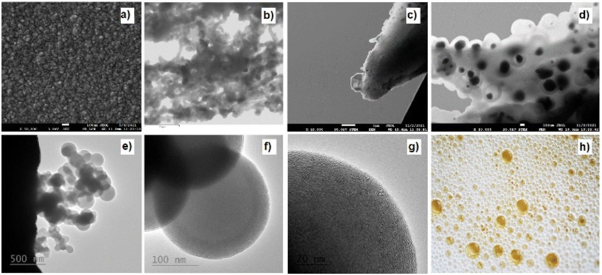 | ||
| Fig. 3 (a) The SEM picture of 1-1050 (b) STEM-observed the chains of carbon nano-mousse in 2-900a, (c) nano-mousse bulk in 3-1050a (d) STEM detail of nano-mousse in 1-1050a, (e) HR-TEM image of nano-mousse formation in 2-500a, (f) HR-TEM individual multiwall sphere detail of a sphere in 2-500a, (g) multi-wall character of 2-1050a in HR-TEM detail, (h) champagne mousse for comparison (copied under Creative Commons license). | ||
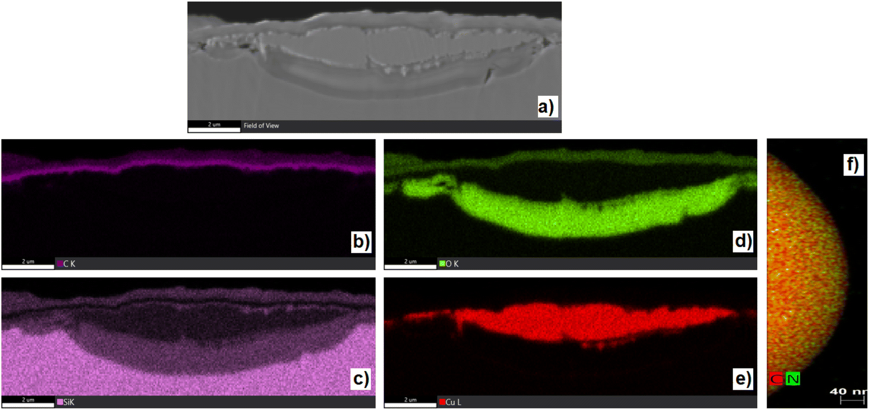 | ||
| Fig. 4 EDS mapping of sample 1-1050b. (a) SEM microscopic image of cross-section of 1-1050b. (b) EDS – K-signal of carbon (c) EDS – K-signal of silicon. (d) EDS – K-signal of oxygen. (e) EDS L-signal of copper (all of the images are taken in the same cross-section). (f) The EDS map of HR-TEM detail of 1-1050a individual sphere of nano-mousse. | ||
XPS measurements revealed that the resulting nano-mousse layers are indeed carbon materials. Apart from carbon making at least 75 atom% of the materials, signals of nitrogen, oxygen, and copper, coming clearly from the substrate (copper sheet), can be spotted in the spectra. Table 1 sums up the recalculated XPS-based elemental composition of samples where copper has been excluded from the calculations. Clear trends can be spotted even in the basic elemental composition. The carbon presence visibly increases with the increasing temperature of the treatment, while nitrogen and oxygen presence decreases with the increasing temperature of the treatment. In particular, oxygen presence is quite surprising as the samples were prepared under an inert atmosphere (nitrogen).
| F d | C (atom%) | N (atom%) | O (atom%) |
|---|---|---|---|
| a Data influenced by Cu LLM and Cu LLM1 peaks due to high signal of copper. | |||
| 1-1050 | 93.7 | 2.6 | 3.7 |
| 1-900 | 88.1 | 7.1 | 4.8 |
| 1-750 | 75.0a | 11.6a | 13.4a |
| 2-1050 | 94.8 | 2.2 | 3.0 |
| 2-900 | 88.7 | 6.2 | 5.1 |
| 2-750 | 84.4 | 10.9 | 4.6 |
| 2-600 | 82.3 | 12.2 | 5.4 |
| 2-500 | 78.2 | 14.8 | 7.0 |
| 3-1050 | 95.2 | 3.0 | 1.8 |
| 3-900 | 90.2a | 5.7a | 4.1a |
O 1s spectra throughout the samples show the oxygen of one binding type (see ESI, Fig. S12 to S41†) with the binding energy ranging from 531.5 eV (1-750) to 532.7 eV (2-1050), which effectively rules out the possibility that CuOx (approx. 529.5 for CuO and approx. 530.5 for Cu2O)36 observed in 1-1050b sample influences the measurement. Therefore, the presence of copper oxides on the EDS mapping is probably ex-post oxidation created by the handling of the samples. On the other hand, the O 1s values resemble the values often observed in the graphene-oxide type of materials.37,38 Therefore, during the cooling of the material, partial oxidation of carbon structure probably took place, yielding some graphene-oxide type of C–O/C![[double bond, length as m-dash]](https://www.rsc.org/images/entities/char_e001.gif) O bonds.
O bonds.
C 1s and N 1s regions give further insight into the structure (Table 2, Fig. S12 to S41, ESI†). C 1s region in all samples is dominated by a signal at around 284.7 eV, which corresponds to C–C/CC bonds in the carbon lattice. Oxidized carbons, C–O/C–N (visible at 284.7 eV), CO/CN (285.4 eV), and COO/CN2 (288.9 eV) tend to decrease with treatment temperature in comparison with a relative amount of C–C/CC bonds. This observation is somewhat paradoxical to the determined elemental composition of the materials (Table 1). Combined with the insight gained by Raman spectra (vide infra), the explanation lies in the quality of the materials. While materials X-1050 appear to be spherical multilayer carbon nanostructures, the structure of lower temperature treated samples reports multiple structural imperfections and disruptions, with relatively small poly-aromatic carbon domains, yet spherical carbonic multi-wall nature prevails (Fig. 3). That means most of the oxygen and hydrogen heteroatoms are bonded in terminal bonds such as –COOH, –CONH2, –OH, –NH2, CO, etc. When heteroatom terminates the structure, it naturally bears only one bond to the carbon lattice; therefore, the number of C-heteroatom bonds is relatively lowered.
| Bond type/sample | C 1s (atom%) | N 1s (atom%) | |||||
|---|---|---|---|---|---|---|---|
| 284.7 eV (C–C/CC) |
285.4 eV (C–N/C–O) | 287.8 eV (CO/CN) |
288.9 eV (COO/CON/CN2) | 398.8 eV (CN–C) |
401.0 eV (C–N–C) | 402.4 eV (NC3) | |
| 1-1050 | 74.0 | 20.3 | 4.4 | 1.3 | 18.0 | 65.3 | 16.7 |
| 1-900 | 75.3 | 19.7 | 2.6 | 1.3 | 14.0 | 86.0 | 0.0 |
| 1-750 | 81.3 | 13.7 | 2.9 | 2.1 | 80.1 | 19.9 | 0.0 |
| 2-1050 | 83.6 | 11.8 | 3.2 | 1.5 | 31.1 | 68.9 | 0.0 |
| 2-900 | 71.6 | 22.2 | 3.6 | 2.6 | 31.5 | 58.5 | 0.0 |
| 2-750 | 78.4 | 14.8 | 4.5 | 2.3 | 39.0 | 55.0 | 6.0 |
| 2-600 | 85.5 | 10.5 | 1.9 | 1.1 | 67.4 | 32.6 | 0.0 |
| 2-500 | 88.2 | 9.0 | 1.6 | 1.2 | 62.0 | 38.0 | 0.0 |
| 3-1050 | 78.9 | 16.8 | 4.2 | 0.1 | 21.9 | 53.8 | 24.3 |
| 3-900 | 75.1 | 18.7 | 4.0 | 2.3 | 26.6 | 73.4 | 0.0 |
This observation is well supported by the trends in the quality of C-heteroatom bonds. While the amounts of more oxidized carbons (signals at 287.8 and 288.9 eV) remain narrowly distributed throughout the samples or slightly increase with the lower temperatures of the treatment, the relative difference in the occurrence of C–heteroatom bond is made by the signal at 285.4 eV, single C–heteroatom bonds. This indicates that while X-1050 samples have a relatively low content of heteroatoms (Table 1), at the same time, they have a relative plurality of C–heteroatom bonds. In other words, heteroatoms are better incorporated into the carbon lattice, and they form fewer terminal moieties.
In general, pyridinic nitrogens (398.8 eV)39 are preferred at lower temperatures, while pyrrolic nitrogens (401.0 eV)40 occur at higher temperatures. Three samples of best pyridine-nitrogen retention are 1-750, 2-600, and 2-500. This suggests pyridin-4-yl radical, anticipated in all three precursors (Fig. 1), is better conserved at lower temperatures (see Section 2.4). Higher temperatures, on the other hand, appear to prefer pyrrolic nitrogen. Graphitic nitrogen (402.4 eV) might be observed sporadically; the best source of it is probably material 3, as was anticipated (see Fig. 1; 24.3 atom% of graphitic nitrogen in 3-1050). Yet, most of the observations from Table 2 cannot be as straightforward as proposed in Fig. 1. An occurrence of relationships between the structure of precursor and the distribution of particular N-enrichment types is evident though.
Normalized average Raman spectra are shown in Fig. 5. It is obvious that sample 1-750 has very strong fluorescence background, thus no baseline correction was performed. The occurrence of fluorescence has been recorded in several samples with low treatment temperatures, yet only in 1-750, it was always as high that it was not possible to further analyze the Raman spectrum. Presence of residues of small organic molecules in the sample, coming from imperfect condensation of the carbon material, can explain this observation.
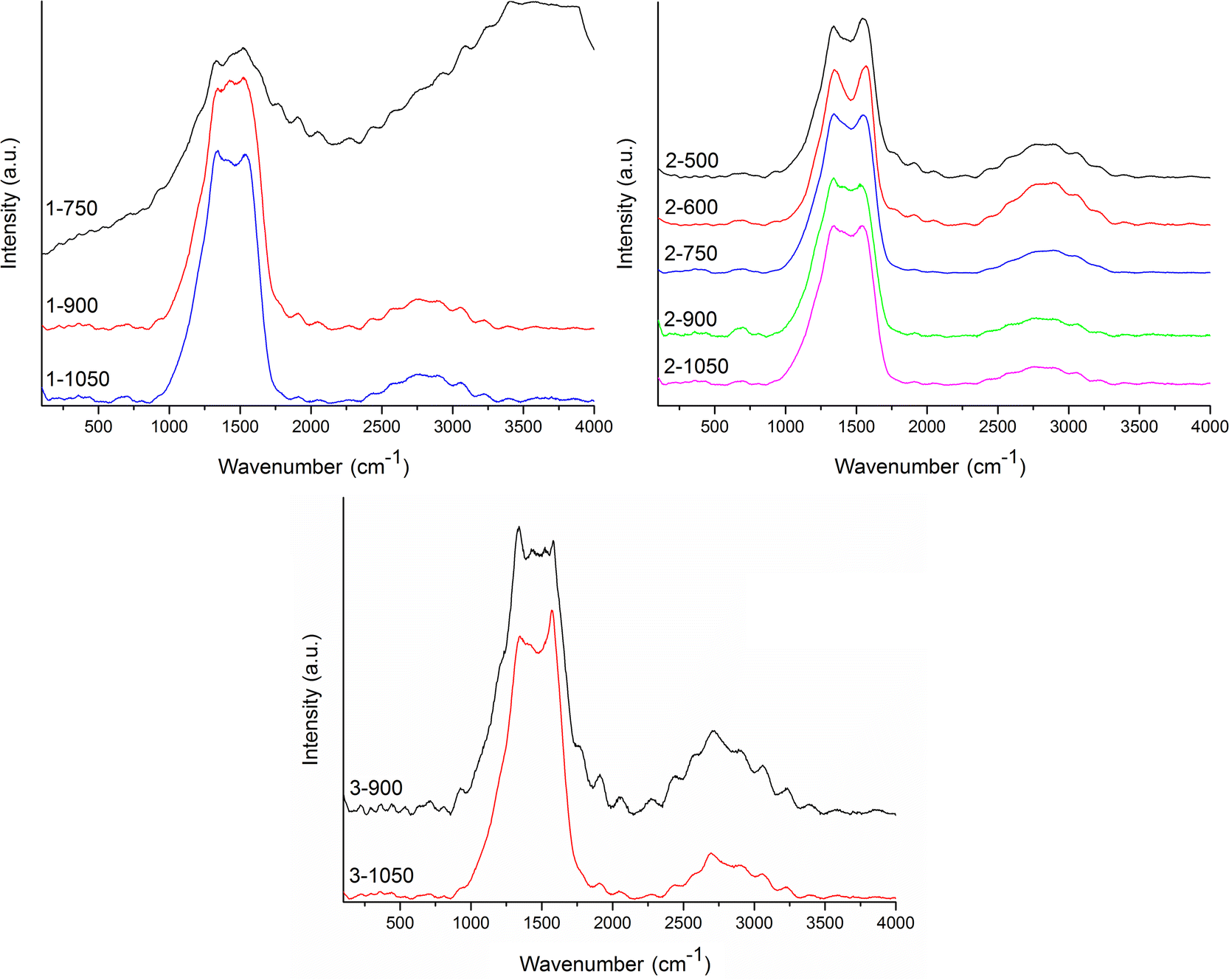 | ||
| Fig. 5 Raman spectra of X-TTT materials. | ||
Overall, Raman spectra were very noisy, yet the pattern of two main bands of a carbon material (GG and D band) is observable. On top of that, all the recorded Raman spectra visibly contain further Raman signals beyond these bands. For this reason, the deconvolution process was performed for all the recorded spectra in the range 800–1900 cm−1 (representative deconvolution Fig. 6, rest of deconvoluted spectra in Fig. S2 to S10 in ESI†) excluding the sample 1-750 (vide supra). Wavenumbers of the deconvoluted bands are summed in Table 3.
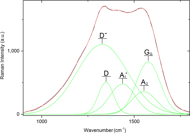 | ||
| Fig. 6 Representative deconvolution of 1-1050. | ||
| Sample/banda | 1-1050 | 1-900 | 2-1050 | 2-900 | 2-750 | 2-600 | 2-500 | 3-1050 | 3-900 |
|---|---|---|---|---|---|---|---|---|---|
| a I Dap/IGap ratio was recorded from intensities of non-deconvoluted Raman spectra as the intensity of apparent maximum in D-part of the spectra (first local maximum of bulky peak) and G-part of spectra (last local maximum of bulky peak). | |||||||||
| Ds | 1239 | 1234 | |||||||
| D− | 1327 | 1318 | 1330 | 1327 | 1325 | 1314 | 1327 | 1327 | |
| D | 1346 | 1363 | 1338 | 1340 | 1340 | 1340 | |||
| A1 | 1416 | 1419 | 1405 | 1426 | 1426 | ||||
| A1+ | 1436 | 1442 | 1453 | ||||||
| A2− | 1470 | 1492 | 1473 | ||||||
| A2 | 1556 | 1544 | 1542 | 1522 | |||||
| GG | 1572 | 1565 | 1576 | 1577 | 1572 | 1586 | 1579 | 1579 | |
| D′ | 1630 | ||||||||
| I Dap/IGapa | 1.02 | 0.96 | 1.00 | 1.04 | 1.01 | 0.98 | 0.98 | 0.91 | 1.05 |
Overall, nine types of peaks were detected during the deconvolutions of Raman spectra. Peaks are denoted Ds, D−, D, A1, A1+, A2−, A2, GG and D′ consistent with their standard descriptions.12,41 The D band is connected to the sample disorder due to the clustering of sp2 bonded carbon atoms. This band was observed in all the samples prepared at 1050 °C (1-1050, 2-1050, and 3-1050), in low-temperature samples coming from material 2 (2-600 and 2-500) and in 3-900 at wavelengths 1338 cm−1 to 1363 cm−1. The GG band arises from the zone center E2g bond stretching mode of graphite and is present in all sp2-bonded carbons. All the samples except of 1-900 bear GG vibration between 1565 cm−1 and 1586 cm−1. In sample 3-900 D′ signal, connected with a heteroatom-caused defect, is also extractable.
Vibration denoted D− was observed in the majority of samples. This vibration occupied a quite narrow region between 1318 cm−1 and 1330 cm−1. It coincided in all of the X-1050 samples and in the low temperature 2-TTT samples with D vibration, while in the rest of the samples except for 3-900, it replaced this vibration. Vibrations at the wavelengths of D− are referred to be connected with curved carbon lattices such as those in carbon nanotubes.42,43 An alternative explanation is disruptions caused by C–H-prolific edges of the structure. Presence of D− vibrations indicates that the spherical character observed in the samples X-1050a (Fig. 3) is probably present in most of the samples (with the possible exception of 3-900). Co-presence of D− and D vibrations indicates that, at least in the samples in question, several layers of curved carbon lattice are present. Thus, according to this, N-doped carbon nano-mousse has a character of interconnected multi-wall carbon spheres.
The family of A-vibrations A1, A1+, A2−, and A2 are assigned as Kekulé modes41,44 of variously curved carbon honeycomb. A1+ and A2 modes relate to more polymeric material with bigger carbon (polyaromatic) domains (>C16) with the occasional presence of heteroatoms, while A1 and A2− point to materials with more lattice imperfections and smaller polyaromatic domains (C10 to C16). Another sign of imperfect materials is the presence of Ds breathing vibration of C6–C10 domains in 1-900 and 3-900 (1239 cm−1 and 1234 cm−1, respectively).
One way of characterizing the overall quality of carbon is through ID/IG ratio. In X-TTT samples, it is not clear which intensities should be taken to construct this ratio. ID−/IG and ID/IG ratios often give conflicting suggestions about the quality of carbon honeycomb, rendering information from them inconclusive. For this purpose, only IDap/IGap is given in Table 3, constructed as the ratio between intensities of apparent maxima in the D-part and G-part of the non-deconvoluted peak. Values of IDap/IGap ratio are around 1.0, suggesting the multi-wall nature of carbon nano-mousse is in good accordance with HR-TEM observations. The trends of IDap/IGap ratios sometimes show somewhat paradoxical behavior when several lower-temperature samples (e.g.2-900, 2-750, 3-900) show higher values than their higher-temperature counterparts. This might not suggest that those samples show better carbon lattice quality for three reasons: i. the results themselves might be, in fact, obtained by random fluctuations of Raman spectra and might, in fact, effectively mean the same value, ii. the presence of A-peaks as a main marker of carbon imperfections often shows otherwise, and iii. their values are influenced by interference of several Raman signals (see Fig. 6).
In that respect, Raman spectra show that carbon structure is the most perfect in samples X-1050 and possibly 2-600 and 2-500, while the rest of the samples made at temperatures lower than 1050 °C are clearly less perfect carbon materials. Strong signs of the curved or spherical surface of carbon structure have been detected, which corresponds well with the microscopic observations (Fig. 3 and 4). Lower temperature samples, with aforementioned exceptions, show a plurality of heteroatom-caused disruptions of the structure and its multiple C–H endings. This corresponds well to the observations made by XPS.
2.3. Ellipsometric characterization of carbon layers
To better understand the properties of new material, the Mueller matrix (MM) ellipsometry of 1-1050b, 2-750b, and 1-1050b samples was carried out to study the optical functions of those carbon layers. To be able to extract valuable data, particular samples of X-TTTb had to be made in series differing in the thickness of particular layers. Luckily, the thickness of the layers appeared to be highly dependent on the weight of the precursor in the CVD-like experiment. Therefore, for each X-TTTb sample, a row of subsamples X-TTTb20, X-TTTb30, X-TTTb40, X-TTTb50, and X-TTTb60 were made, where the numbers at the end of the code indicate the input weight (in mg) of particular precursor. In the case of 2-750 and 3-1050 samples (Table 4), only a part of the subsamples was included in the fitting of optical functions; in the case of 1-1050, a whole row of subsamples could be used.| Sample | Thickness (nm) | Roughness (nm) |
|---|---|---|
| 1-1050b20 | 38.00 | 4.50 |
| 1-1050b30 | 46.70 | 3.40 |
| 1-1050b40 | 51.90 | 3.00 |
| 1-1050b50 | 54.20 | 2.70 |
| 1-1050b60 | 57.60 | 3.20 |
| 2-750b20 | 32.42 | 4.86 |
| 2-750b30 | 67.18 | 0.00 |
| 2-750b40 | 84.65 | 0.10 |
| 2-750b50 | 78.31 | 2.47 |
| 3-1050b40 | 23.41 | 3.47 |
| 3-1050b50 | 39.84 | 0.10 |
Each subsample had a copper side and the silicon side (see Methods), both of which were covered by the N-doped carbon layer with identical ellipsometric properties as far as they were observable. The copper sides, though, suffered from high roughness of the N-doped carbon layer caused by partial melting of the copper layer and formation of copper drops (see Section 2.2, Fig. 4), which deteriorated the possibility of fitting the optical functions of N-doped carbon layer directly in the copper-side. Instead of that, ellipsometric data were collected on the silicon side. The MM-elements for particular subsamples were measured at multiple incident angles of 45°–60° with a 5° step. In order to reduce the fitting parameters, multi-sample analysis was performed, in which the optical function is considered the same for all of the subsamples of particular X-TTT material (e.g., all 1-1050bYY subsamples were considered differently thick layers of identical material 1-1050b). Fig. 7 displays the measured and modelled MM-elements of subsample 1-1050b30. A good agreement of the fitted model with the measured data is clearly visible. Table 4 further describes the modelled thicknesses and roughnesses of subsamples selected for the model fitting. The crucial result of MM-ellipsometry is the optical functions of the material displayed as the dependence of refractive index (n) and extinction coefficient (k) on the wavelength for particular samples X-TTTb. Fig. 8 shows those functions for materials 1-1050b, 2-750b, and 3-1050b. The course, shape, and values of refractive indices and extinction coefficients quite resemble similar optical functions of highly conductive carbon materials deposed on silicon-based or metallic matrices.45 High values of refractive index in 1-1050b (always higher than those of graphite or graphene) imply that this material is of high optical conductivity and probably is performing as a conductor or low-bandgap semiconductor. Those observations are ever more visible on the optical function of real, but mainly imaginary part of the dielectric function. Fig. 8 compares those functions with those of a metal-like allotrope of carbon-graphite. All three samples show an increase of imaginary part towards the infrared region corresponding to the Drude model of electric conductivity.46 In the case of 1-1050b, this increase is clearly higher than that of graphite, suggesting 1-1050b is, in fact, a better conductor than graphite from the optical standpoint as it has better absorption of free charges. All in all, all of the optical functions suggest the metal-like or graphite-like conductive behavior of X-1050b materials, which is certainly an unanticipated property of such carbon materials.
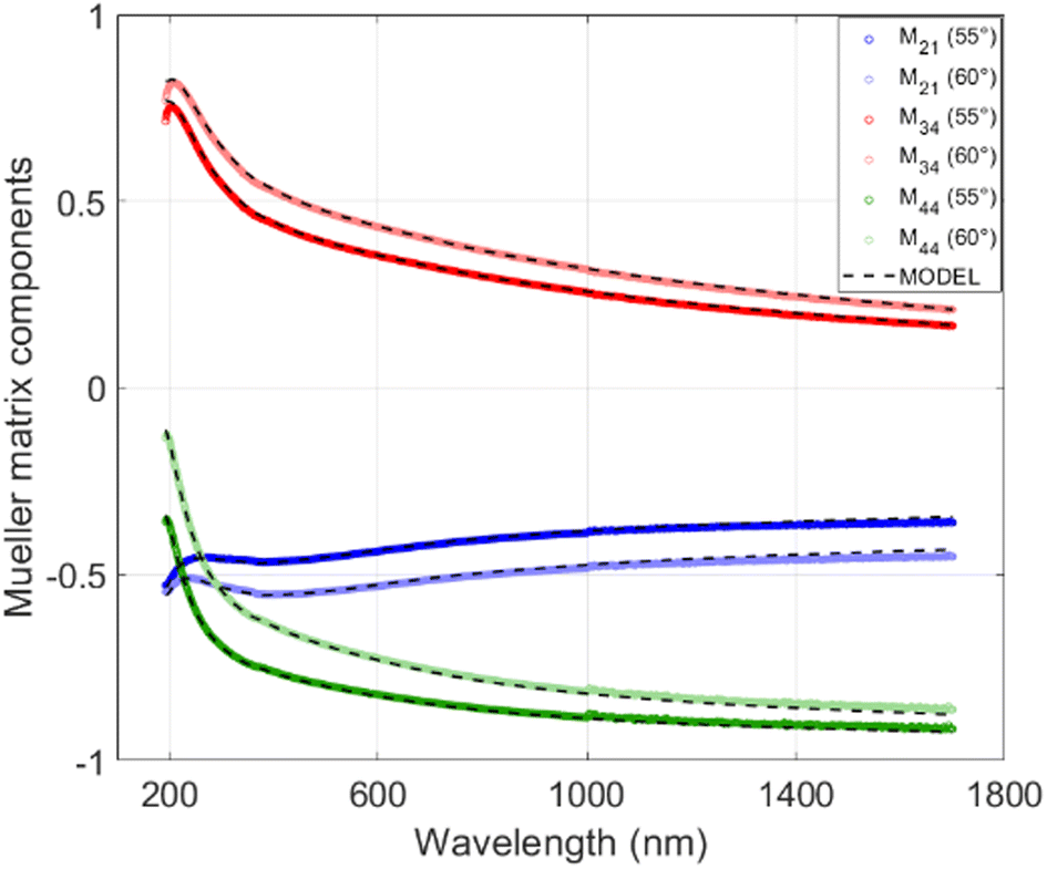 | ||
| Fig. 7 Mueller matrix elements of sample 1-1050b30. | ||
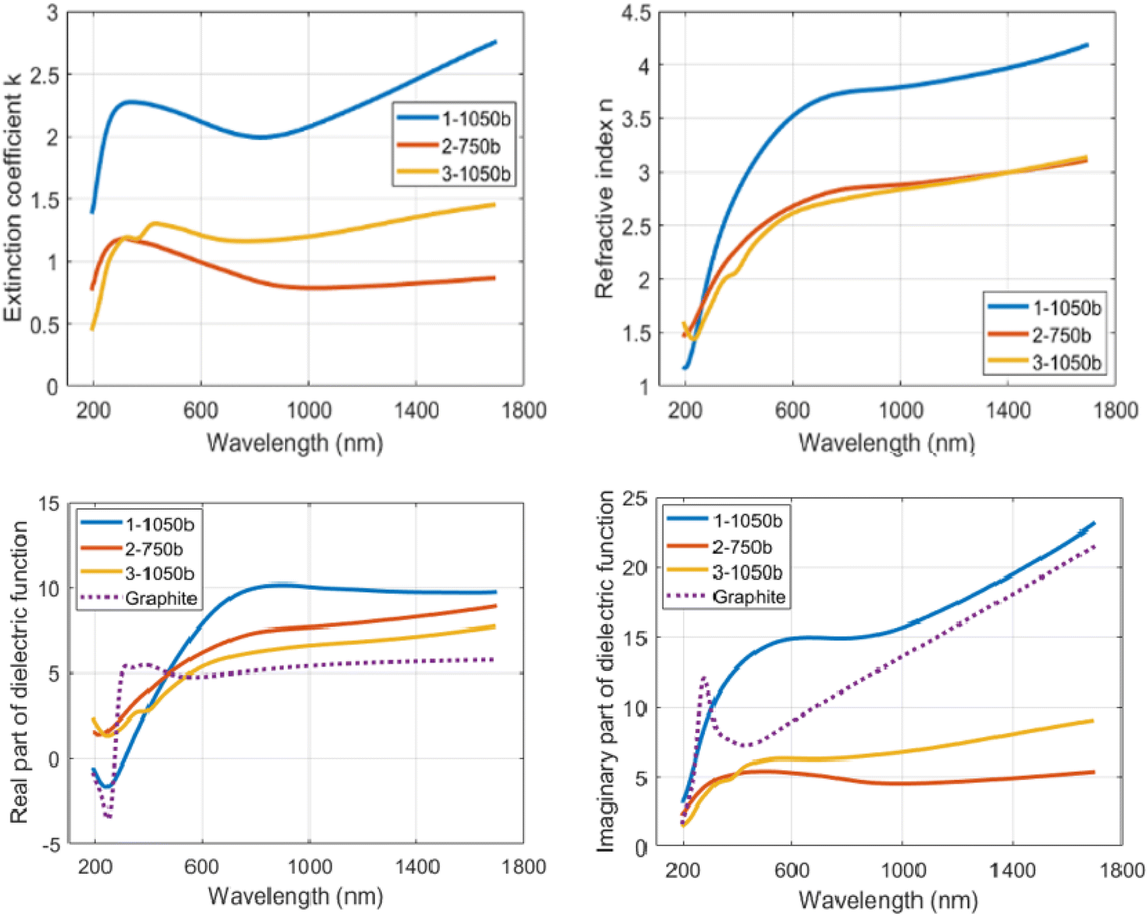 | ||
| Fig. 8 Optical functions of 1-1050b, 2-750b and 3-1050b as function of extinction coefficient (k) and refractive index (n) d real and imaginary part of dielectric function on the wavelength graphite values in dielectric functions are taken from reference 58. | ||
2.4. Discussion on the nature of gained material and hypothesis of its emergence
From the performed analyses and characterizations, N-doped carbon nano-mousse appears to be composed of spherical nano-textural multi-wall units of diameter approx. 200 nm, which are interconnected and/or clustered through sharing some of their walls. Unlike most of the carbon nano-forms, the spherical structure of the units stays conserved to an extent;11,31 unlike most of the classical carbon hollow spheres, no template is needed for their creation, and individual spheres are distinguishable from the rest of the material. In this case, spheres are embedded in a more amorphous form of N-doped carbon or interconnected by such material.The mechanism of creation of N-doped carbon nano-mousse from the precursors is, despite gathered evidence, still unclear. However, there are a couple of key points that stand out. First, the presence of metal or metalloid (nano-mousse matter was also observed on silicon parts of substrates, see Section 2.3). Second, precursors probably enter the reaction as chemical individuals, and the chemical changes occur presumably in the direct vicinity of the metal surface (see Section 2.1). In accordance with the valid theory of carbon formation during the classical CVD process,47 the chemical steps should be based on radical reactions and rearrangements. Thus, homolyses of C–N, C–C, and C–H bonds, preferably the first two as their homolytic dissociation energy is lower, are the initial steps of the reactions. The metal/metalloid surface probably plays an important role as a source/quencher of single-electron transfers restoring the balance of electrons.
From this, an initial hypothesis of the mechanism of formation of nano-mousse can be extracted. The precursor, when approaching the copper surface, starts to homolytically decompose to first order radicals such as pyridin-4-yl radical, (pyridin-4-yl)aminyl radical, and similar radicals preferably sourcing from the C–C and C–N homolysis. Those radicals may further decompose/rearrange to second order radicals, such as cyano, carbon diimidyl, and (cyano)ethynyl (as pictured at Fig. 9).
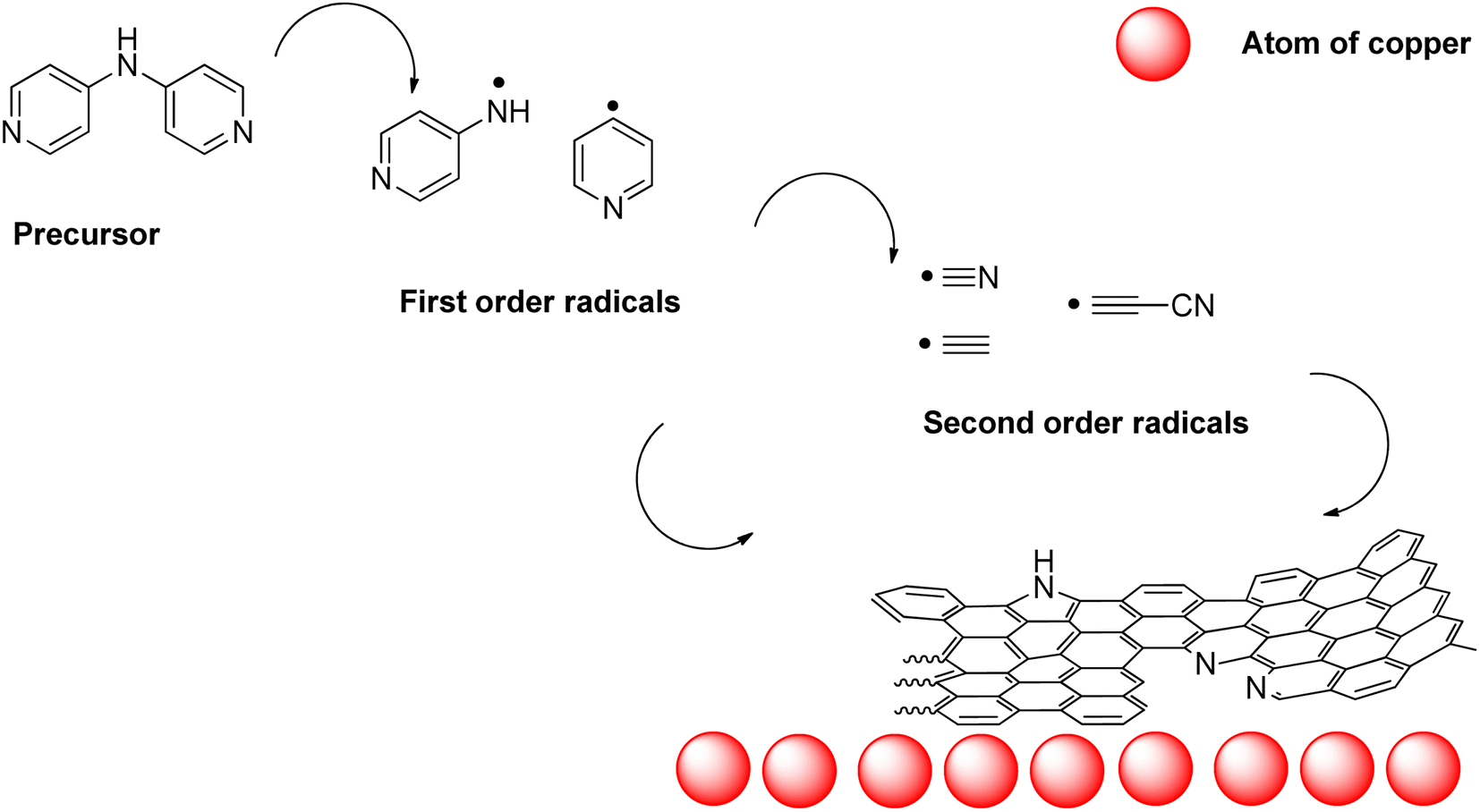 | ||
| Fig. 9 Proposed mechanism of N-doped carbon nanofoam formation. | ||
The first order radicals and second order radicals impact the copper substrate forming carbon matter containing nitrogen atoms. Upon the formation of the carbon honeycomb, gaseous waste products such as ammonia, hydrogen cyanide, cyanamide, etc., are formed. The interconnected system of multi-wall spheres might be partially explained by the emergence of those gases. On the other hand, this phenomenon is insufficient in explaining the overall highly spherical character of nano-mousse (this is a typical mechanism of forming carbon nano forms different from nano-mousse). A force strong enough to produce spherical symmetry has to be present. From the gathered evidence, it is not straightforward which particular force it might be. Among those which should be taken into account, mechanical forces are unlikely to bring this kind of result. From that, deductively, an occurrence of temporary charges (e.g. emerged from single-electron transfer processes) and the necessity of their stabilization is the best explanation for the time being. However, a deeper study of the mechanism of occurrence of this material is needed.
3. Conclusions
Ten materials 1-1050, 1-900, 1-750, 2-1050, 2-900, 2-750, 2-600, 2-500, 3-1050, and 3-900, and their surrogate materials prepared for individual analyses were reproducibly prepared by the CVD-like procedure from precursors 1, 2, and 3 on copper-based substrates. This method of preparation yields 100 nm to 400 nm thick layers of N-doped carbon material of, to the best knowledge of authors, yet the unparalleled texture and rather unique structure and optoelectronic properties. Moreover, the thickness of the layers, along with the degree and the nature of N-doping, appears to be manageable by both the structure of the precursor and the temperature of CVD/like treatment. This is best demonstrated in its chemical properties as the pyridinic-nitrogen enrichment is clearly directed by the nature of the precursor and by the temperature, showing that the medium-sized N-containing molecules might offer an advantage in targeted N-doped carbon formation. This material has been called N-doped carbon nano-mousse as it resembles the mousse on champagne in the STEM images.N-doped carbon nano-mousse is a macroscopically metal-tinged film, optical conductor, or low band gap semiconductor. Microscopically, it is composed of probably multi-wall spherical carbon units of approx. 200 nm diameter interconnected by an amorphous or quasi-amorphous phase of carbon. Chemically, it bears three types of N-enrichment (pyrrolic, pyridinic, and graphitic nitrogens) in various ratios depending on the precursor and temperature of the treatment. Remarkable first-screening optoelectronic observations of 1-1050b, 2-750b, and 3-1050b hint at its potential use in oxygen-reduction reactions, supercapacitors, and perhaps even in photo-or electro-catalysis.
In conclusion, N-doped carbon nano-mousse is a material with already recognizable great potential and is definitely worth further studying, which is now performed by our group.
4. Methods
4.1. Used materials and general methods
Pyridine (Penta, p. a. quality), 4-aminopyridine (Sigma-Aldrich, reagent grade), phosphorus chloride (Sigma-Aldrich, reagent grade), solution of NaClO (25%, technical grade), cyanuric chloride (VWR chemicals, reagent grade), acetonitrile (VWR chemicals, reagent grade), ethyl acetate (VWR chemicals, pure), hexane (Sigma-Aldrich–Merck, mixture of isomers, reagent grade), silica gel (VWR, MS 20 μm, for flash chromatography), ethanol (VWR chemicals, absolute), helium for GC/MS analyses (SIAD, 6.0 grade), hydrogen for CVD-like experiments (SIAD, 6.0 grade), argon both as inert in chemical syntheses (SIAD, 5.0 grade) and for CVD-like experiments (SIAD, 5.0 grade), copper substrates (copper foil, Puratronic®, Alfa Aesar, 0.025 mm thick, 99.999%) were purchased from particular suppliers, and used in the preparations, experiments, and analyses as obtained without any purification, if not further stated otherwise.The purity and identity of precursors 1 and 2 has been verified on GC/MS (Agilent Technologies 7890N; mass detector Agilent Technologies 5975C; DB-XLB 30 m × 0.25 mm x 0.25 μm), purity and identity of precursor 3 has been verified on HPLC/MS (HPLC Shimadzu; MS QTRAP 6500 + Sciex).
4.2. Syntheses of precursors
Precursors 1, 2, 3 (Fig. 1) were synthesized and purified following one-step procedures known from the literature (references 48–50, respectively) without any modification from commercial precursors (mentioned in the previous Section). Identities and purity of precursors were confirmed by GC/MS and HPLC/MS methods.4.3. CVD-like procedure
CVD apparatus had a design corresponding to standard CVD apparatuses used elsewhere.51,52 Photos of the apparatus are provided in ESI (Fig. S1†).Precursors 1, 2, and 3 were placed near the bottom of a small test tube (10 cm, 10 ml), and at the mouth of the test tube, a copper-based substrate (sheet of copper, approx. 8 × 12 mm) was placed. Such a test tube was placed in the glass tube of the CVD apparatus (photo Fig. S1†). The external heater was placed in such a way that the copper sheet was covered by it, whereas the precursor was outside the area covered by the heater. The apparatus has been evacuated (down to a pressure lower than 1 mBar) and filled with argon (260 ml min−1). After 2 min of argon influx, hydrogen was let to influx the apparatus (50 ml min−1). After that, the external heater was switched on and let heat up to a temperature of 1050 °C (heating rate 40 °C min−1) to reduce the trace impurities on the copper surface. After 40 min, the external heater was left to cool down to the temperature of the particular experiment (1050 °C, 900 °C, 750 °C, 600 °C or 500 °C, respectively), if needed, and the heater was moved towards the precursor at the rate of 0.5 cm min−1 up to the point the precursor was in the geometrical center of the heater. Subsequently, the heating was turned off, and the apparatus was let to cool down to a temperature below 100 °C. The copper sheets were visibly covered by a film having a “steel” color (photo Fig. 2). Such gained samples were subjected to all the analyses further mentioned in this paper.
4.4. Raman microspectroscopy
All samples were measured by Smart Raman System XploRA™ (Horiba, France) with the same experimental setup. The laser (532 nm, green line, 100 mW) was reduced to 10% of the initial laser beam intensity. Grating with 600 grooves/mm and objective with magnification 100× was used. Samples were each measured in 16 different points approximately in the middle of the sample, where each point was 100 μm apart and altogether formed a square. Automatic baseline correction was performed in the LabSpec software. For better graphic comparison, spectra were normalized and deconvoluted in the Origin software.4.5. Microscopic measurements
STEM samples were prepared by the CVD-like procedure similar to the procedure described in Section 4.3. Instead of copper sheets, TEM-grids (Electron Microscopy Sciences; 25p/k, copper, uncoated) of high-purity copper were used.The surfaces and cross-sections of the layers were studied using the JEOL JSM-7610F Plus (JEOL, Japan) Scanning Electron Microscope (SEM) equipped with STEM detector DEBEN (DEBEN UK Ltd). The carbon layers and particles were shown in STEM mode and SE mode with the detection of the secondary electrons.
Argon ion polishing PECS II system (GATAN, United States) was used for the preparation of cross-section to map main elements. The chemical compositions of the layers were determined using an energy dispersive X-ray spectrometer (EDX, Oxford Instruments).
An atomic force microscope (AFM, LiteScope™) was used in semi-contact mode to measure the thickness of the layers in combination with the material contrast of SEM (CPEMTM).
High Resolution Transmission Electron Microscope (HR-TEM) Titan G2 60-300 (FEI) with an image corrector at an accelerating voltage of 80 kV was used to record the HR-TEM images. Those were taken with a BM UltraScan CCD camera (Gatan). Energy Dispersive Spectrometry (EDS) was performed in Scanning TEM (STEM) mode by Super-X system with four silicon drift detectors (Bruker). STEM images were taken with HAADF detector 3000 (Fishione).
4.6. XPS measurements
The XPS measurements were carried out with the PHI 5000 VersaProbe II XPS system (Physical Electronics, Chanhassen, MN, USA) with a monochromatic Al-Kα source (15 kV, 50 W) and photon energy of 1486.7 eV. All spectra were measured in the vacuum of 1.4 × 10⁻⁷ Pa and at 20.5 °C. The analyzed area on the sample had a spot of 100 μm in diameter. The survey spectra were measured with a pass energy of 187.850 eV and a step of 0.8 eV, while for the high-resolution spectra, a pass energy of 23.500 eV and a step of 0.2 eV was used. Dual beam charge compensation was used for all measurements. The spectra were evaluated with the MultiPak (Ulvac-PHI, Inc., Chanhassen, MN, USA) software. All binding energy (BE) values were referenced to the carbon peak C 1s at 284.80 eV.4.7. Spectroscopic ellipsometry measurements
In ellipsometry measurements, the polarizer-compensator-sample-compensator-analyzer configuration of the experimental measurement was applied to collect all 16 elements of the Mueller matrix (M).53 This transforms the Stokes vector upon transmission or reflection from the sample according to Sout = MSin, where Sin and Sout are the Stokes vectors of the incident and reflected field, respectively. The most common definition of the Stokes vector is written in the following way S = [S_0,S_1,S_2,S_3]T = [Ix + Iy, Ix – Iy, I45° – I−45°, IR – IL]T (T denotes transposed vectors), where Ix, Iy, I45°, and I−45° are directly measurable intensities linearly polarized along x, y, +45°, and −45°, respectively, and IR and IL denote intensities of right and left circularly polarized light.54 The ellipsometer uses a combination of a halogen bulb and a deuterium lamp as a light source in the UV-NIR spectral region from 0.74 eV to 6.42 eV (193–1700 nm). The beam is collimated by an achromatic lens and then passes through a fixed MgF2 Rochon polarizer and through achromatic rotating Fresnel rhomb compensators, which are in both arms of the ellipsometer. The detector consists of two spectrometers: (i) Si CCD detector for UV-vis spectral range and (ii) InGaAs photodiode array for NIR region. Sample holder enables rotation of the sample around the surface normal. In reflection, the angle of incidence φ measured from the surface normal can be varied from 20°–80°. This technique is fast, non-destructive, and very sensitive to the thin films parameters such as thickness, optical functions, and surface roughness.55 For these reasons, set of the carbon layers with different precursor weights on the Cu/Si wafers was prepared to overcome the difficulties with the copper sheets.The critical step involved in fitting ellipsometric data to a given structural model is the proper parametrization of the dispersion of the unknown energy-dependent complex optical functions ñ(E) = n − iκ of the carbon layers. We have used B-spline parametrization, which is based on a set of basic functions describing the complex structure in the absorption spectra (κ), while simultaneously providing the Kramers–Kronig consistent dispersion spectra (n).56 The roughness of the samples is modeled by Bruggeman's effective medium approximation of 50% bulk material and 50% void.57 Standard non-linear iterative optimization analysis called the Levenberg–Marquardt least square algorithm is applied in fitting procedures.
Author contributions
M. Lesňák carried out most of the experimental laboratory work, therefore falling under the contributor role of investigation according to CRediT taxonomy. D. Cvejn came up with the idea of investigation and wrote a better portion of the manuscript, therefore falling under the contributor roles of conceptualization, methodology, and writing – original draft. M. Petr measured and interpreted the XPS spectra, therefore falling under the contributor roles of investigation and data curation. P. Peikertová measured all of the Raman microspectrometry, interpreted them via deconvolution, and provided useful consultations on the final version of the manuscript, therefore, falling under the contributor roles of investigation, data curation, and writing – review & editing. R. Gabor recorded most of the microscopic data used in the publication and coordinated the outsourced measurements falling under contributor roles of investigation and data curation. T. Fördös carried out all the spectroscopic-ellipsometric experiments and their interpretation falling under contributor roles of investigation and data curation. P. Czernek mastered the CVD-like apparatus and was deeply involved in the experimental methodology, falling under the contributor role of methodology. D. Plachá provided laboratory equipment, chemicals, and funding for the experimental work, was involved in final manuscript editing, and overall supervised and coordinated the work, falling under contributor roles of project administration, resources, supervision, and writing – review & editing.Conflicts of interest
There are no conflicts to declare.Acknowledgements
This work was supported by the Doctoral Grant Competition VSB–Technical University of Ostrava, Reg. No. CZ.02.2.69/0.0/0.0/19_073/0016945, in Operational Programme Research, Development and Education under the project DGS/TEAM/2020-007 “Study of the Effect of Additives on Emissions during the Combustion of Alternative Fuels”. Physical part of the project has been supported by IT4Innovations national supercomputing center – path to exascale project (CZ.02.1.01/0.0/0.0/16_013/0001791). Experimental results were accomplished by using Large Research Infrastructure ENREGAT supported by the Ministry of Education, Youth and Sports of the Czech Republic under project no. LM2018098. Dr Alexandr Martaus is to be gratefully acknowledged for his enormous efforts to record XRD patterns of the samples, even though those results never made it to the manuscript due to the lack of conclusiveness. MSc. Ondřej Tomanec is to be equally gratefully acknowledged for providing HR-TEM imagery on impossibly short notice.References
- S. R. Stoyanov, A. V. Titov and P. Král, Coord. Chem. Rev., 2009, 253, 2852–2871 CrossRef CAS.
- M. Kaur, M. Kaur and V. K. Sharma, Adv. Colloid Interface Sci., 2018, 259, 44–64 CrossRef CAS PubMed.
- X. Zheng, J. Deng, N. Wang, D. Deng, W. H. Zhang, X. Bao and C. Li, Angew. Chem., Int. Ed., 2014, 53, 7023–7027 CrossRef CAS PubMed.
- R. Czerw, M. Terrones, J. Charlier, X. Blase, B. Foley, R. Kamalakaran, N. Grobert, H. Terrones, D. Tekleab, P. M. Ajayan, W. Blau, M. Rühle and D. L. Carroll, Nano Lett., 2001, 1, 457–460 CrossRef CAS.
- J. Shui, M. Wang, F. Du and L. Dai, Sci. Adv., 2015, 1, 1–8 Search PubMed.
- Y. Ito, C. Christodoulou, M. V. Nardi, N. Koch, H. Sachdev and K. Müllen, ACS Nano, 2014, 8, 3337–3346 CrossRef CAS PubMed.
- X.-F. Li, K.-Y. Lian, L. Liu, Y. Wu, Q. Qiu, J. Jiang, M. Deng and Y. Luo, Sci. Rep., 2016, 6, 23495 CrossRef CAS PubMed.
- Y. Xue, H. Chen, J. Qu and L. Dai, 2D Mater., 2015, 2, 044001 CrossRef.
- Z. Xing, Z. Ju, Y. Zhao, J. Wan, Y. Zhu, Y. Qiang and Y. Qian, Sci. Rep., 2016, 6, 26146 CrossRef CAS PubMed.
- M. Min, S. Seo, Y. Yoon, K. Cho, S. M. Lee, T. Lee and H. Lee, Nanoscale, 2016, 8, 17022–17029 RSC.
- J. C. Lytle, J. M. Wallace, M. B. Sassin, A. J. Barrow, J. W. Long, J. L. Dysart, C. H. Renninger, M. P. Saunders, N. L. Brandell and D. R. Rolison, Energy Environ. Sci., 2011, 4, 1913–1925 RSC.
- Y. S. Zou, Q. M. Wang, H. Du, G. H. Song, J. Q. Xiao, J. Gong, C. Sun and L. S. Wen, Appl. Surf. Sci., 2005, 241, 295–302 CrossRef CAS.
- L. Wang, Y. Wang, T. Xu, H. Liao, C. Yao, Y. Liu, Z. Li, Z. Chen, D. Pan, L. Sun and M. Wu, Nat. Commun., 2014, 5, 5357 CrossRef CAS PubMed.
- J. Xu, F. He, S. Gai, S. Zhang, L. Li and P. Yang, Nanoscale, 2014, 6, 10887 RSC.
- Z. Wang, X. Xiong, L. Qie and Y. Huang, Electrochim. Acta, 2013, 106, 320–326 CrossRef CAS.
- L. Zhang and Z. Xia, J. Phys. Chem. C, 2011, 115, 11170–11176 CrossRef CAS.
- A. Khan, M. Goepel, J. C. Colmenares and R. Gläser, ACS Sustain. Chem. Eng., 2020, 8, 4708–4727 CrossRef CAS.
- J. Zhao, X. Chen and J. R. H. Xie, Anal. Chim. Acta, 2006, 568, 161–170 CrossRef CAS PubMed.
- Y.-K. Sun and H. Kim, US Pat., US10593951B2, 2017 Search PubMed.
- M. Inagaki, M. Toyoda, Y. Soneda and T. Morishita, Carbon, 2018, 132, 104–140 CrossRef CAS.
- C. Maddi, F. Bourquard, V. Barnier, J. Avila, M. C. Asensio, T. Tite, C. Donnet and F. Garrelie, Sci. Rep., 2018, 8, 1–13 CAS.
- D. Deng, X. Pan, L. Yu, Y. Cui, Y. Jiang, J. Qi, W.-X. W. X. Li, Q. Fu, X. Ma, Q. Xue, G. Sun and X. Bao, Chem. Mater., 2010, 23, 183–191 Search PubMed.
- N. Li, Z. Wang, K. Zhao, Z. Shi, Z. Gu and S. Xu, Carbon, 2010, 48, 255–259 CrossRef CAS.
- F. Zeng, L. Yang, Y. Pan, M. Xu, H. Liu, M. Yu, M. Guo and C. Yuan, Electrochim. Acta, 2019, 325, 134903 CrossRef CAS.
- A. Capasso, T. Dikonimos, F. Sarto, A. Tamburrano, G. De Bellis, M. S. Sarto, G. Faggio, A. Malara, G. Messina and N. Lisi, Beilstein J. Nanotechnol., 2015, 6, 2028–2038 CrossRef CAS PubMed.
- Z. Wang, L. Qie, L. Yuan, W. Zhang, X. Hu and Y. Huang, Carbon, 2013, 55, 328–334 CrossRef CAS.
- D. Yuan, T. Zhou, S. Zhou, W. Zou, S. Mo and N. Xia, Electrochem. commun., 2011, 13, 242–246 CrossRef CAS.
- Z. Zhao, Z. Zhu, H. Zhang, W. Fang, W. Jiang, S. Lin and Y. Yang, Appl. Surf. Sci., 2020, 534, 147631 CrossRef CAS.
- J. Ahn, Y. Song, J. E. Kwon, S. H. Lee, K. S. Park, S. Kim, J. Woo and H. Kim, Mater. Sci. Eng. C, 2019, 102, 106–112 CrossRef CAS PubMed.
- H. Wang, T. Maiyalagan and X. Wang, ACS Catal., 2012, 2, 781–794 CrossRef CAS.
- Z. Li, S. Gao, H. Mi, C. Lei, C. Ji, Z. Xie, C. Yu and J. Qiu, Carbon, 2019, 149, 273–280 CrossRef CAS.
- K. N. Wood, R. O'Hayre and S. Pylypenko, Energy Environ. Sci., 2014, 7, 1212 RSC.
- A. J. Marsden, P. Brommer, J. J. Mudd, M. A. Dyson, R. Cook, M. Asensio, J. Avila, A. Levy, J. Sloan, D. Quigley, G. R. Bell and N. R. Wilson, Nano Res., 2015, 8, 1–16 CrossRef.
- R. Yadav and C. K. Dixit, J. Sci.: Adv. Mater. Devices., 2017, 2, 141–149 Search PubMed.
- B. Giroire, M. Ali Ahmad, G. Aubert, L. Teule-Gay, D. Michau, J. J. Watkins, C. Aymonier and A. Poulon-Quintin, Thin Solid Films, 2017, 643, 53–59 CrossRef CAS.
- M. F. Al-Kuhaili, Vacuum, 2008, 82, 623–629 CrossRef CAS.
- A. M. Abdelkader, C. Vallés, A. J. Cooper, I. A. Kinloch and R. A. W. Dryfe, ACS Nano, 2014, 8, 11225–11233 CrossRef CAS PubMed.
- R. Al-Gaashani, A. Najjar, Y. Zakaria, S. Mansour and M. A. Atieh, Ceram. Int., 2019, 45, 14439–14448 CrossRef CAS.
- F. Zheng, Y. Yang and Q. Chen, Nat. Commun., 2014, 5, 1–10 Search PubMed.
- J. Liu, Y. Zhang, L. Zhang, F. Xie, A. Vasileff and S. Z. Qiao, Adv. Mater., 2019, 31, 1–10 Search PubMed.
- M. Ayiania, E. Weiss-Hortala, M. Smith, J. S. McEwen and M. Garcia-Perez, Carbon, 2020, 167, 559–574 CrossRef CAS.
- N. Hayazawa, T. Yano, H. Watanabe, Y. Inouye and S. Kawata, Chem. Phys. Lett., 2003, 376, 174–180 CrossRef CAS.
- A. Y. Gerasimenko, G. N. Ten, D. I. Ryabkin, N. E. Shcherbakova, E. A. Morozova and L. P. Ichkitidze, Spectrochim. Acta - A: Mol. Biomol., 2020, 227, 117682 CrossRef CAS PubMed.
- M. W. Smith, I. Dallmeyer, T. J. Johnson, C. S. Brauer, J. S. McEwen, J. F. Espinal and M. Garcia-Perez, Carbon, 2016, 100, 678–692 CrossRef CAS.
- M. A. El-Sayed, G. A. Ermolaev, K. V. Voronin, R. I. Romanov, G. I. Tselikov, D. I. Yakubovsky, N. V. Doroshina, A. B. Nemtsov, V. R. Solovey, A. A. Voronov, S. M. Novikov, A. A. Vyshnevyy, A. M. Markeev, A. V. Arsenin and V. S. Volkov, Nanomaterials, 2021, 11, 1–13 CrossRef PubMed.
- S. Chen, P. Kühne, V. Stanishev, S. Knight, R. Brooke, I. Petsagkourakis, X. Crispin, M. Schubert, V. Darakchieva and M. P. Jonsson, J. Mater. Chem. C, 2019, 7, 4350–4362 RSC.
- M. Kumar and Y. Ando, J. Nanosci. Nanotechnol., 2010, 10, 3739–3758 CrossRef CAS PubMed.
- F. Bures, D. Cvejn, K. Melanova, L. Benes, J. Svoboda, V. V. Zima, O. O. Pytela, T. T. Mikysek, Z. Ruzickova, I. V. Kityk, A. Wojciechowski, N. AlZayed, F. Bureš, D. Cvejn, K. Melánová, L. Beneš, J. Svoboda, V. V. Zima, O. O. Pytela, T. T. Mikysek, Z. Růžičková, I. V. Kityk, A. Wojciechowski and N. AlZayed, J. Mater. Chem. C, 2016, 4, 468–478 RSC.
- S. Verma, V. Vajpayee, S. M. Lee, H. J. Jung, H. Kim and K. W. Chi, Inorganica Chim. Acta, 2012, 387, 435–440 CrossRef CAS.
- B. Xu, C. Yajun, Q. Lijun, W. Xiao and N. Pei, CN106046389A, 2016.
- A. Bachmatiuk, F. Schäffel, D. Plachá, G. Martynková Simha, N. Ioannides, T. Gemming, T. Pichler, R. Kalenczuk J. and M. Rümmeli H., Fuller. Nanotub. Carbon Nanostructures, 2010, 18, 37–44 CrossRef CAS.
- J. Pang, A. Bachmatiuk, I. Ibrahim, L. Fu, D. Placha, G. S. Martynkova, B. Trzebicka, T. Gemming, J. Eckert and M. H. Rümmeli, J. Mater. Sci., 2016, 51, 640–667 CrossRef CAS.
- R. W. Collins and J. Koh, J. Opt. Soc. Am. A, 1999, 16(8), 1997–2006 CrossRef.
- M. Losurdo, A. S. Brown and G. Bruno, in Ellipsometry at the Nanoscale, Springer Berlin Heidelberg, 2013, pp. 453–491 Search PubMed.
- T. Fördös, K. Postava, H. Jaffrès, D. Quang To, J. Pištora and H. J. Drouhin, Appl. Phys. Lett., 2018, 112, 221106 CrossRef.
- A. H. Sihvola, Electromagnetic Mixing Formulas and Applications, The Institution of Electrical Engineers, London, 1999 Search PubMed.
- B. Johs and J. S. Hale, Phys. Status Solidi (A) Appl. Mater. Sci., 2008, 205, 715–719 CrossRef CAS.
- E. D. Palik, Handbook of Optical Constants of Solids, Elsevier, Amsterdam, The Nederlands, 2012 Search PubMed.
Footnote |
| † Electronic supplementary information (ESI) available. See DOI: https://doi.org/10.1039/d2ta07947j |
| This journal is © The Royal Society of Chemistry 2023 |