
CuBi2O4 nanocrystals integrated with polyaniline nanobelt arrays for weak light photomultiplication type photodetector†
Anshika
Singh
 *a,
Pratima
Chauhan
a,
Arpit
Verma
b and
Bal
Chandra Yadav
b
*a,
Pratima
Chauhan
a,
Arpit
Verma
b and
Bal
Chandra Yadav
b
aAdvanced Nanomaterials Research Laboratory, U.G.C. Centre of Advanced Studies, Department of Physics, University of Allahabad, Prayagraj-211002, India. E-mail: anshikasingh@allduniv.ac.in; mangu167@yahoo.co.in
bNanomaterials and Sensors Research Laboratory, Babasaheb Bhimrao Ambedkar University, Lucknow-226025, U.P., India
First published on 29th November 2022
Abstract
In this paper, a novel flexible photodetector based on emerging p-type CuBi2O4 and p-type conducting polymer polyaniline is fabricated. The conducting polymer is directly coated on the surface of CuBi2O4via a facile and low-cost in situ polymerization approach. The morphological investigation of CuBi2O4-polyaniline nanohybrid material shows that nanobelts and the material interface are responsible for the high rate of charge carrier generation. X-ray diffraction analysis confirmed that the inorganic material CuBi2O4 intercalated in the polyaniline matrix. The I–V measurement was carried out on the prepared device in the range of −50 V to +50 V and the photoresponse at an illumination intensity of 50 μW cm−2. The flexible device shows high-performance photodetection with a high external quantum efficiency (EQE) of 1.824 × 10³ %, a high photoresponsivity of 5.381 A W−1 and a detectivity of 6.02 × 10¹¹ Jones at only 1 V. Because of the straightforward device design and low-cost fabrication process, this study offers a feasible way for manufacturing organic–inorganic high-performance low-intensity photon detectors.
1 Introduction
Organic–inorganic nanohybrid photodetectors (OINPDs) have seen significant advancements in the fields of optical communication, artificial intelligence, environmental monitoring, biomedical imaging, and sensing in recent years.1–6 In current history, studies on OINPDs with high sensitivity and high integration have drawn more attention.5,7,8 The energy bandgap of the semiconductor materials used to fabricate the photodetector device must be carefully designed to meet the operational wavelength because the wavelength of interest covers the ultraviolet (UV) to the infrared (IR) range.7,9,10 Flexible electronics have attracted a lot of interest due to their fascinating properties, such as biocompatibility, flexibility, light weight, shock resistance, softness, and transparency, for their potential use in future displays, wearable technology, and energy-storage devices.11 Due to their potential suitability for numerous novel applications in multiple new fields, including portable electronics, aeronautical science, and civil engineering, flexible photodetectors have recently risen to the forefront of current research. The detectability of photodetectors, for instance, has been limited by the enormous amount of dark current coming from the gapless band structures of graphene, which is only one of several difficulties they encounter. On the other hand, photodetectors built with 2D semiconductor materials such as transition metal dichalcogenides (TMDCs) have the advantage of low dark current because of the significant Schottky barrier between the metal electrodes and the semiconductors. The device often needs to be biased to produce a detectable photocurrent which calls for an external power source.12–15 Since it is impracticable to provide or replace a power source for each device, only self-driven or ultralow-power photodetectors are suitable for applications like wearable medical monitoring and outdoor environmental sensing for wireless sensor networks.7,16–21 Self-driven photodetectors have been proposed using a wide range of device topologies. The photovoltaic effect, which enables the p–n junction to generate a sizable photocurrent without an external bias, makes it the semiconductor that is most frequently explored.22,23 The metal–semiconductor–metal (MSM) photodetector devices and varied metal electrodes allowed for the achievement of different Schottky barrier heights for self-driven photodetection. However, making any of these devices is a challenging task. We must still construct a reliable, low-cost, low-dark current and self-driven photodetector.18,24,25 Using CuBi2O4 deposited on n-Si and a p–n heterojunction, Zewei Wu et al. recently created a photodetector that shows a remarkable photoresponsivity of 1.69 × 10⁴ mA W−1 at an applied bias of zero potential.21CuBi2O4 is a newly developed p-type semiconductor that is intended to be used as a photocathode in the photoelectric synthesis of solar fuel.26 CuBi2O4 is a native p-type semiconductor with an optical band gap between 1.5–1.8 eV. Also, CuBi2O4 exhibits polaron transport, which significantly lowers charge mobility and shortens the diffusion length of the photo carriers to 10–52 nm.27,28 This directly limits the adequate CuBi2O4 layer thickness for photo conversion due to the blue region of the spectrum's higher absorption coefficient, which would produce photo carriers closer to the illumination surface when using broadband illumination.29 The Cu2+ oxidation state and 3d9 open-shell structure are adopted by the Cu ions in CuBi2O4. Recent studies on open shell metal oxides such as Fe2O330,31 and Cu3V2O8 show that localized d–d transitions at the metal cation are less efficient in converting photons to photocurrent than charge transfer transitions from the O2− ligand to the metal cations.29,32 Although d–d transitions through the Mott–Hubbard gap are essential in the absorption of visible light into photo-generated carriers in open-shell metal oxides, they do not necessarily lead to extractable photocurrent.26
An optical (analog or digital) signal can be transformed into an electrical signal by a photodetector, primarily in the form of current or voltage.1,6,19,33–36 An external voltage creates an electric field that segregates, gathers, and transports photogenerated electron–hole (e–h) pairs to external electronics.37,38 To separate, collect, and transfer photogenerated e–h pairs to external electronics, an external voltage power supply produces an electric field. High-performance IR photodetectors based on III–V compound semiconductors always encounter challenges with high preparation costs, low temperature operating requirements and improvements in in-plane uniformity. New materials for detection and manipulation must be developed immediately to address this.33,39,40 To solve the problems of high dark current and poor absorption efficiency, the photodetectors should use localized electron and photon manipulations.37,41 Dark current can be efficiently suppressed using techniques such as electrical manipulations by ferroelectric, built-in, and gate electric fields.30,42,43 By combining with other materials, the response spectrum of a photodetector based on hybrid materials could likewise be widened to the infrared region. Poor photoresponsivity can occur from the high exciton binding energy making it difficult to separate and gather e–h pairs.44 Therefore, breaking the exciton binding energy in the hybrid materials can improve the photodetection performance. Nanohybrid photodetectors are gaining popularity due to their straightforward design, broad material variety, and ability to process huge areas. Numerous people are becoming interested in creating panchromatic, ultraviolet, near-infrared, and color-selective photodetectors.45,46 Due to their low background noise and short response times, photodiode type nanohybrid photodetectors are excellent for practical applications such as optical communication, remote control, and image sensing. The fundamental issue with conventional device structures is their inability to achieve extraordinarily high EQE in low-light situations.3,45
The photomultiplication (PM) phenomenon produces an EQE value greater than 100%, which spreads many charge carriers across a photodetector for each incident photon.2,47 Several methods have been successfully implemented for generating PM in nanohybrid materials, including co-planar structures with or without trap-assisted injection and sandwich structures with trap-assisted charge carrier tunneling injection.45,48–50 Opposing charge carriers constantly move through the active layer and are drawn to the appropriate electrode in nanohybrid materials, where photo-generated electrons or holes are trapped or inhibited.45 Due to the relatively high Schottky barrier for hole injection and the absence of continuous electron transport channels in the active layers, nanohybrid photodetectors with little dark current have high EQE values.45 Due to inherent biodegradable qualities CuBi2O4-polyaniline nanohybrid was used for photodetection experiment on textile substrate.51 Cotton textile is composed of cellulose i.e., a type of glucose which naturally degrades both aerobically and anaerobically. Table 1 lists the defining characteristics of the CuBi2O4-polyaniline nanohybrid photodetector device along with a study of the literature on various active material based photodetectors.
| Active materials | Bias voltage (V) | Wavelength | Flexibility | Rise/decay time | Responsivity A W−1 | Detectivity (Jones) | EQE (%) | Ref. |
|---|---|---|---|---|---|---|---|---|
| PANI/ZnO | 0 | UV | No | 0.11/1.45 ms | 0.56 | — | — | 52 |
| NZF-PANI | 5 | Visible | Yes | 0.9/0.8 s | 24.980 | 3.735 × 10¹² | — | 36 |
| WS2-PAM | — | 365 nm | Yes | 0.422/0.543 s | 1.374 | 1.526 × 10¹² | 465.93 | 53 |
| WSe2-PANI | 15 | 670 nm | Yes | 0.9/1 s | 0.056 | — | — | 4 |
| SnSe2/PEDOT:PSS | 0.1 | UV | Yes | 16 | 0.73 | — | — | 6 |
| Visible | 221 | 0.69 | ||||||
| NIR | 274 | 0.67 | ||||||
| ZnO/polyaniline | — | — | No | — | 0.024 | — | 7.47 | 54 |
| MoS2-PAM | — | 365 nm | No | — | 60.09 | 4.96 × 10¹¹ | 20.373 | 55 |
| TiO2/PC71BM/PEDOT:PSS | 350 | No | 60 ms/<1 μs | 33 | 1.60 × 10¹¹ | — | 56 | |
| Ga2O3/PANI | 246 | No | 0.34/8.14 ms | 21 | 1.50 × 10¹¹ | — | 35 | |
| Se/PANI | 0 | 610 | No | 4.50/2.84 ms | 120 | 3.78 × 10¹¹ | 34 | |
| Se/PPY | 0.35/16.97 ms | 70 | ||||||
| Se/PEDOT | 1.00/9.78 ms | 5.5 | ||||||
| CuBi2O4-polyaniline | 1 V | 365 nm | Yes | 1.35/0.97 | 5.381 | 6.016 × 10¹¹ | 1.824 × 10³ | This work |
| 5 V | 8.194 | 9.161 × 10¹¹ | 2.778 × 10³ |
2 Experimental section
2.1 Materials used
Bismuth nitrate (Bi(NO3)3·5H2O), >99%, copper nitrate (Cu(NO3)2·3H2O), >99%, sodium hydroxide (NaOH), p-toluene sulfonic acid (CH3C6H4SO3H, p-TSA), aniline (C6H5NH2), >99.5%, and ammonium peroxy disulfate ((NH4)2S2O8), >99%, were purchased from Fisher Scientific, India. All the chemicals were used as procured without any further purification process.2.2 Synthesis procedure for CuBi2O4 nanocrystals (NCs)
CuBi2O4 was synthesized by the hydrothermal method which was previously reported by Wang Yi et al.57 In the synthesis procedure of CuBi2O4, typically 0.97 g of Bi(NO3)3·5H2O was dissolved in 5 mL of acetic acid and 0.24 g of Cu(NO3)2·3H2O was dissolved in 25 mL of ethyl alcohol. Then the two solutions were mixed and the NaOH solution was added under magnetic stirring at room temperature until the pH reached 14. Subsequently, the above mixture was transferred into a 100 mL Teflon-lined steel autoclave and then maintained at a temperature of 120 °C for 5 h. The obtained product was washed by centrifugation at 3500 rpm with ethanol and distilled water three times, respectively, and then dried in an oven for 12 h at 80 °C.2.3 Incorporation of CuBi2O4 in the polyaniline matrix
For the incorporation of CuBi2O4 in the polyaniline matrix, we used the in situ chemical oxidation polymerization approach. In the first step of the synthesis, 1 M p-TSA solution was made in 50 mL of double distilled water. This p-TSA solution was separated in the two beakers in equal volumes. In the first beaker 0.2 g of CuBi2O4 was dissolved by magnetic stirring at 3500 rpm. In the second beaker, 1 M solution of (NH4)2S2O8 was made for the initiator solution. In the second step, 5 mL of aniline monomer was dissolved in the CuBi2O4 solution and stirred for 1 h. After this initiator solution was added drop-wise to the precursor solution, this solution first turned gray and finally dark green. This solution was placed in a ventilated place for 24 h so that all the residual monomers could also convert into the polymer. After this, this greenish solution was filtered with Whatman filter paper and washed until the extract pH became neutral.3 Results and discussion
3.1 Surface morphological and elemental analysis
Scanning electron (SEM) micrographs were used to observe the morphologies of CuBi2O4-polyaniline treated on cotton fibers. The prepared solution of CuBi2O4-polyaniline coated on the cotton substrate formed nanofibers at 500 μm and made the cotton surface rougher as shown in Fig. 1a. It is clearly seen that the cotton fibers are covered with a uniform and dense film of CuBi2O4-polyaniline nanohybrid material as depicted in Fig. 1(b and c). It shows nanobelt-like structures at 50 μm and 10 μm, respectively. The deposition of the sample CuBi2O4-polyaniline on the cotton substrate creates an interface between the materials and substrate as clearly seen in the micrographs presented in Fig. 1d and the cotton fibers could lead to better charge carrier generation resulting in an excellent performance of the device. SEM micrographs of the pure CuBi2O4 NCs powder are shown in ESI Fig. S1.† | ||
| Fig. 1 Scanning electron micrographs of CuBi2O4-polyaniline at a scale of (a) 500 μm, (b) 50 μm, (c) 10 μm and (d) 1 μm on the textile substrate. | ||
X-ray photoelectron spectroscopy (XPS) was carried out for the analysis of the surface and chemical states of the CuBi2O4-polyaniline nanohybrid. The XPS survey suggested the chemical composition of Cu 2p, Bi 4f, O 1s, N 1s and C 1s in CuBi2O4-polyaniline sample as represented in Fig. 2a. The core-level spectra of Cu 2p show two peaks centered at 951.91 eV and 934.37 eV for Cu 2p1/2 and Cu 2p3/2 which corresponded to the 2+ oxidation state of Cu as shown in Fig. 2b. In Fig. 2c, the core level spectra of Bi 4f show binding energies of 164.5 eV and 160.18 eV which corresponds to the Bi 4f5/2 and Bi 4f7/2 states, respectively, and confirms the 3+ oxidation state. Also, binding energy of S 2p at 168.89 eV suggests S 2p3/2 as depicted in Fig. 2c. The O 1s spectrum shows two peaks with a binding energy of 532.96 eV and 532.10 eV for metal hydroxide and metal carbonates/metal–oxygen bonding, respectively, as shown in Fig. 2d. The core level spectrum of N 1s shows two peaks at 400.37 eV and 398.57 eV for C-NH2 and metal nitrides in the sample as shown in Fig. 2e. The core spectrum of C 1s was deconvoluted into three peaks located at 284.70 eV for C–C/C![[double bond, length as m-dash]](https://www.rsc.org/images/entities/char_e001.gif) C, 285.62 eV for C–O/C–N and 286.42 eV for C–O–C as shown in Fig. 2f.
C, 285.62 eV for C–O/C–N and 286.42 eV for C–O–C as shown in Fig. 2f.
 | ||
| Fig. 2 (a) XPS survey spectrum and (b) core spectra of Cu 2p, (c) Bi 4f, (d) O 1s, (e) N 1s and (f) C 1s in the CuBi2O4-polyaniline sample. | ||
3.2 Structural analysis
The structural analysis of pristine CuBi2O4 and CuBi2O4-polyaniline samples were analyzed by X-ray diffraction (XRD). In Fig. 3a, XRD of CuBi2O4 NCs shows a tetragonal crystal structure belonging to the space group P4/ncc and all the peaks corresponding to their (hkl) planes are perfectly matched with the JCPDS file no. 42-0334.21,26,27,57 As we can see in Fig. 3b, the XRD pattern of CuBi2O4-polyaniline shows that only one peak with a strong intensity corresponds to CuBi2O4 NCs shown in the CuBi2O4-polyaniline nanohybrid system and all other peaks of CuBi2O4 disappear as the polymer covered the surface of the CuBi2O4 NCs.19,35,36,54Fig. 3c shows the unit cell of CuBi2O4 and Fig. 3d shows the crystal structure of CuBi2O4 corresponding to the (211) Braggs plane.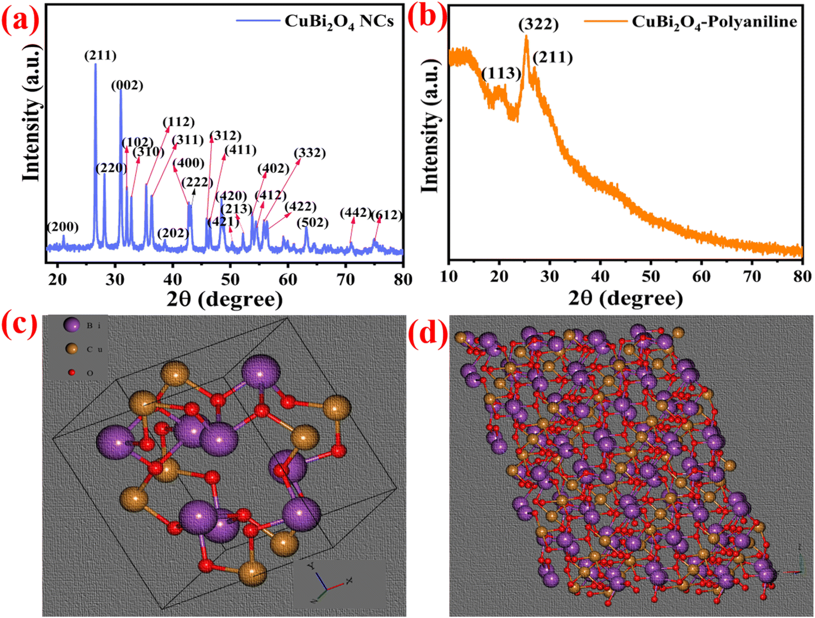 | ||
| Fig. 3 (a) X-ray diffraction patterns of CuBi2O4 nanocrystals, (b) CuBi2O4-polyaniline, (c) unit cell of CuBi2O4 and (d) (211) Braggs plane of the CuBi2O4 crystal. | ||
3.3 Optical analysis
The FTIR spectra of CuBi2O4 and CuBi2O4-polyaniline are shown in Fig. 4a. CuBi2O4-polyaniline shows characteristic bands at 1546 cm−1 and 1477 cm−1 suggesting a CC stretching vibration of quinoid (Q) i.e. (NQN) and benzenoid ring (B) i.e., (N–B–N) respectively.36,54 The bands at 1403 cm−1, 1293 cm−1 and 1232 cm−1 shows C–N stretching of the secondary aromatic ring.19,35,54 The band at 1097 cm−1 shows aromatic C–H in-plane bending vibrations and the bands in the range of 900–600 cm−1 show aromatic C–H out-of-plane bending vibrations.36 The bands at 3121 cm−1 and 2928 cm−1 show sp2 and sp3 hybridized carbon. The vibrational band at 3673 cm−1 depicts water present in the sample. The vibrational bands of CuBi2O4 at 1392 cm−1 and 520 cm−1 represent Bi–O and Cu–O respectively.21,26,27,57 The bands at 3484 cm−1 and 1520 cm−1 show the hydroxyl group (–OH) in the CuBi2O4 sample.
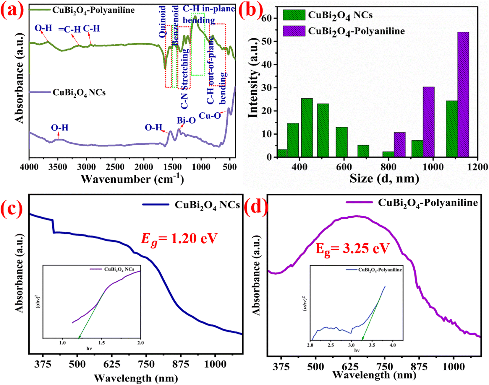 | ||
| Fig. 4 (a) FTIR spectra of CuBi2O4 NCs and CuBi2O4-polyaniline, (b) particle size distribution graph of CuBi2O4 NCs and CuBi2O4-polyaniline, (c) UV-visible absorption spectrum and Tauc plot of CuBi2O4 NCs and (d) UV-visible absorption spectrum and Tauc plot for CuBi2O4-polyaniline. | ||
In the dynamic light scattering (DLS), a monochromatic beam of light encounters a solution containing nanoparticles/macromolecules and light scatters in all directions as a function of the size and shape of the dispersed material. In the light intensity fluctuations caused by the Brownian motion of the dispersant, scattered light is analyzed, and the diffusion coefficient is related to the hydrodynamic radius. Such a Brownian motion of the particles also depends on the temperature, size and viscosity.58 When the movement of particles over a time range is monitored, information on the size of dispersed particles can be obtained, as large particles diffuse slowly, resulting in similar positions at different time points, compared to tiny particles which move faster and therefore do not adopt a specific position.59 From the analysis of the DLS data presented in Fig. 4b, it can be seen that NCs are distributed in the range of 200–1000 nm, whereas NCs of CuBi2O4 are incorporated in the polyaniline structure in the range of 800–1200 nm.
The optical properties of the prepared materials were evaluated by using UV-visible absorbance spectroscopy. The absorbance spectra of CuBi2O4 NCs and CuBi2O4-polyaniline samples dispersed in dimethyl sulfoxide (DMSO) were recorded in the range of 325–1100 nm. The optical band gap of the as prepared materials was determined by using the relation as given in eqn (1):
| αhυ = K(hν − Eg)m | (1) |
3.4 Experimental measurements
A schematic diagram for the photodetection set-up is shown in Fig. 5a which consists of a light source, electrometer and data acquisition system. In an MSM device in which a CuBi2O4-polyaniline treated cotton substrate has two co-planar silver (Ag) electrodes on the fabric,40 when the MSM device is subjected to an electric potential difference, holes are produced from the semiconductor layer to the metal at one of the electrodes, enabling the current to flow forward. The electrodes receive some electric voltage while the operation is being carried out. The collection of charge carriers, exciton dissociation, and photon harvesting all significantly impact the photodetector devices' response.60 When an external bias potential is provided, the semiconductor is completely depleted of carriers (see Fig. 5c), but it still possesses a peak energy barrier for holes.61,62 Charge traps have been successfully used to realize interfacial trap-assisted charge tunneling injection from the external circuit, resulting in the development of PM type photodetectors.60,63,64 The accumulation of photogenerated holes trapped close to the interface between the CuBi2O4-polyaniline material and Ag electrodes, which may be reasonably understood as the cause of this PM phenomenon, triggers the injection of electrons.65 Due to the presence of bi-continuous charge transport channels in the active layers, the generally reported photodetectors can only function under reverse bias and exhibit a relatively high dark current density. One of the ingenious method for developing PM type photodetectors is trap-assisted charge tunneling injection.66 The interfacial band bending caused by trapped electrons in PC71BM near the Al electrode is responsible for the photodetector device using PC71BM as the electron trap in a P3HT matrix exhibiting an EQE of 16![[thin space (1/6-em)]](https://www.rsc.org/images/entities/char_2009.gif) 700% at 380 nm at a potential bias of −19 V.65 For effective hole tunneling injection from the external circuit, trapped photogenerated electrons in the active layer can generate a Coulomb field that causes interfacial band bending when illuminated by light. To increase the detectability for weak light detection, interfacial trap-assisted hole tunneling injection can be effectively improved under a significant applied potential drift.63–66
700% at 380 nm at a potential bias of −19 V.65 For effective hole tunneling injection from the external circuit, trapped photogenerated electrons in the active layer can generate a Coulomb field that causes interfacial band bending when illuminated by light. To increase the detectability for weak light detection, interfacial trap-assisted hole tunneling injection can be effectively improved under a significant applied potential drift.63–66
 | ||
| Fig. 5 (a) The schematic diagram for photodetection measurement. (b) Band diagram under vacuum and dark conditions. (c) Band diagram on applying external bias and under dark conditions. (d) Band diagram on applying external bias and under ambient atmospheric conditions. (e) Band diagram on applying external bias and illumination under ambient atmospheric conditions. | ||
A band diagram for the dark and illumination conditions is also depicted in Fig. 5(d and e). Fig. 5c indicates the band structure of the device on applying potential drift and under dark conditions; in this, a built-in electric field is generated in the device from the positive to the negative electrode. A depletion area forms between oxygenated vacancies and the material surface under ambient atmospheric conditions due to the adsorption of some oxygen species (O2−, O−, O2−) on the material surface and the electrode-material junction. When illumination is applied to the material, these oxygenated vacancies are removed from the surface along with the generation of e–h pairs. As depicted in Fig. 5e, the electrodes capture light induced e–h pairs under sufficient potential drift, and an elevated amount of photocurrent in comparison to the dark level is seen. On illumination of light, e–h couples move from the valence band to the conduction band, whereas in nanohybrid materials, this transition can also happen from defect states to the conduction band. In high band gap and nanohybrid materials, photocurrent is predominantly produced through valence band to conduction band transitions since photon energy cannot directly excite an electron from the valence to the conduction band. When the light is turned off, the conduction band electrons and holes recombine through the recombination sites or band-to-band annihilation.67 The use of top illumination in conjunction with gold contacts that are both incredibly thin and slightly transparent is another option. Since the carriers are generated closer to the contact, the achievable detection bandwidth is often larger with top illumination.68 Considering that a trap-assisted tunneling process dominates current transport in the device at the reverse biased Schottky barrier, we think the effects can be qualitatively characterized. In this model, we assume that the deep-level states are nearly continuous. The conditions associated with the contaminated layer threading dislocations that reach the surface and material imperfections combine to form these traps.33 The current–voltage (I–V) characteristics make it abundantly evident that the current increases as the bias voltage increases in low-intensity and high-intensity illumination environments. A notable increase in photocurrent suggests that the CuBi2O4-polyaniline material and Ag electrodes have good ohmic contact as shown in Fig. 6a and the semi-logarithmic graph of CuBi2O4-polyaniline is presented in the inset image (Fig. 6a). At an illumination intensity of 50 μW cm−2 the photoresponse of the materials in the range of 1 V to 50 V is presented in Fig. 6b.
 | ||
| Fig. 6 (a) Current–voltage characteristics (I–V) in the range of −50 V to +50 V and semi-logarithmic graph as shown in the inset image. (b) Photoresponse at different potential voltages. (c) Photoresponse at different illumination intensities. (d) Rise and decay time at an illumination intensity of 50 μW cm−2 at 1 V. (e) Stability of the photodetector device for 600 s and (f) flexibility of the textile photodetector device at 1 V with illumination intensity of 50 μW cm−2. | ||
or evaluating the performance of the photodetector device, photoresponsivity is the most significant figure of merit. The ratio of photogenerated current to incident optical power per unit area is referred to as the photoresponsivity of the photodetector as given in eqn (2):
 | (2) |
 | (3) |
 | (4) |
The CuBi2O4-polyaniline nanohybrid's photodetector rise time and decay time are defined as the time interval for the transient photocurrent increasing from 10% to 90% of the maximum photocurrent and the time interval for transient photocurrent falling from 90% to 10%, respectively. It can be evaluated by the exponential fitting of the rise and decay function of the time-dependent photoresponse curves as given in eqn (5) and (6), respectively, and was found to be 1.35 s and 0.97 s, respectively as depicted in Fig. 6d.
| I(t) = Idark(e−t/τr) | (5) |
| I(t) = Idark(1 − e−t/τd) | (6) |
The rapid response of the photodetector should be attributed to the electron traps near the Ag electrode being filled in when the incident light is turned on, resulting in the rapid increase in photocurrent. Trapped electrons near the Ag electrode will take some time to be recombined with the injected holes when the incident light is turned off, leading to the relatively slow decrease in photocurrent. The stability of the CuBi2O4-polyaniline nanohybrid textile substrate based photodetector device is exceptionally high at lower voltage and lasts for up to 600 s as represented in Fig. 6e at 1 V with an illumination intensity of 50 μW cm−2. Additionally, since photodetector devices are made from a textile substrate, their flexibility is also measured at three radii of curvatures, as seen in Fig. 6f. The probability of the generation of an exciton for a single photon, which contributes to the photocurrent is defined as the external quantum efficiency,70 as given in eqn (7):
 | (7) |
For an illumination intensity of 50 μW cm−2, the EQE of the photodetector device was 1.111 × 10⁴ % at an applied voltage of 50 V and it decreased to 1.824 × 10³ % for an applied potential of 1 V, which means that under the lower potential difference a lower number of excitons are collected at the electrodes, as represented in Fig. 7a. This is comparable to the report by Zhang et al. where ultraviolet narrowband photomultiplication type organic photodetectors with Fabry–Pérot resonator architecture exhibit an EQE of 9300% at 350 nm.71 The augmentation of hole-tunneling injection and hole transport ability brought on by the growth of the internal electric field in the device is responsible for the significant increase in EQE values with the increase of applied bias.64,71,72 Typically, the EQE for p–n junction type devices is less than 100%, but in this case, the PM EQE of the MSM type CuBi2O4-polyaniline nanohybrid photodetector device exceeded 100%. These adaptable devices can be used in study areas where lower irradiance detection is necessary since the greater EQE enables us to detect low-intensity photons.64,71–73
 | ||
| Fig. 7 (a) Responsivity and EQE vs. applied voltage. (b) Detectivity and NEP vs. applied voltage. (c) LDR and on-off ratio vs. applied voltage. (d) Responsivity and EQE vs. illumination intensity. (e) Detectivity and NEP vs. illumination intensity. (f) LDR and on-off ratio vs. illumination intensity. | ||
Similar to the responsivity of the photodetector device, EQE also decreases on increasing the illumination intensity as depicted in the graph in Fig. 7d. The EQE values of the photodetector device are greater than 100%, which shows that the photodetector device has an internal gain, which is a need for the construction of high-performance photodetectors. On light illumination, e–h couples in the depletion area, where electrons move more quickly than holes, are activated, causing an accumulation of holes at the electrodes.74 However, the partially attracted electrons do not recombine with the trapped holes and are carried away by the strong electric field. The trapped holes draw electrons from the opposite electrode. As a result, the accumulation of holes may result in a reduction in the Schottky barrier, an essential element in defining responsiveness.75 However, the leftover holes can not only result in a decreased Schottky barrier height, but they can also prevent charge recombination and draw more outer electrons into the electrode so they can be neutralized. As a result, there is a sizable gain and a nearly linear voltage dependent responsiveness.76
How effectively the photodetector works in terms of the reciprocal of the noise equivalent power is described by a metric called detectivity given by the formula in eqn (8):
 | (8) |
The higher detectivity suggested that the photodetector device is more sensitive to weak light signals. The highest detectivity of this device was found to be 3.665 × 10¹² Jones at an applied bias of 50 V as presented in Fig. 7b, whereas at an illumination intensity of 375 μW cm−2, detectivity was only found to be 1.596 × 10¹¹ Jones as shown in Fig. 7e. This means that on increasing the illumination intensity of light, detectivity of the photodetector device decreases, indicating that this device is more suitable for weak light detection in comparison to high illumination detection.
The current generated in the absence of illumination determines the slightest detectable light signal. The lowest observable light power is referred to as noise equivalent power. The definition of the linear dynamic range is the ability of the photodetector to adequately capture the variation in light intensity as given in eqn (9):
 | (9) |
The optical input power that results in an additional output power that is identical to that of the device power for a specific bandwidth is known as the noise-equivalent power of the device as given in eqn (10):
 | (10) |
Since that power level is roughly the minimum input power level that can be reliably recognized when averaging the signal over a time of the order of one second, a low NEP is desirable. NEP sometimes known as electrical noise is produced by various causes including Johnson or shot noise in photodetector devices.77 NEP of the photodetector device was found to be 3.051 × 10⁻⁷ W at the 50 V with the illumination intensity of 50 μW cm−2. On increasing the illumination intensity, NEP of the photodetector device also increases at an illumination intensity of 100 μW cm−2, NEP was observed to be 3.549 × 10⁻⁶ W, whereas for an illumination intensity of 375 μW cm−2 it was found to be 7.003 × 10⁻⁶ W. Another important parameter, LDR, was found to 17.565 dB, which is higher among all the measurement. On increasing the applied potential bias of the device, LDR also increases as shown in Fig. 7c. In contrast, on increasing the intensity, this LDR decreases as shown in Fig. 7f. Qualitative parameters of our photodetector device at 50 μW cm−2 in the range of 1–50 V bias voltage are given in Table S1† and different intensities at 1 V are also tabulated in the Table S2.† It is therefore proposed that the CuBi2O4-polyaniline nanohybrid photodetector device on the textile substrate is more suitable for weak light or low-intensity photons detection since the figures of merit shows that on high illumination intensity of light; photoresponsivity, EQE and detectivity decreases.
4 Conclusions
In this study, CuBi2O4 was effectively synthesized using a hydrothermal process, and the obtained material was then employed for in situ polymerization using an aniline monomer. The textile substrate is then used to treat CuBi2O4-polyaniline which produces structures that resemble nanofibers at 500 μm and nanobelts at 10 μm. The photodetection measurement also utilized a textile substrate that had been materially processed. On the flexible and biodegradable substrate, the MSM device exhibits excellent performance. The photodetection measurement shows EQE of 1.824 × 10³ % at a lower bias of 1 V and 1.11 × 10⁴ % at 50 V. An interesting fact about the CuBi2O4-polyaniline photodetector device is that on increasing the illumination intensity of light, the EQE of the device reduces to 4.84 × 10² %.Author contributions
Anshika Singh: writing – original draft, conceptualization, methodology, validation, investigation, resources. Pratima Chauhan: supervision, review and editing. Arpit Verma: conceptualization, visualization and discussions. Bal Chandra Yadav: visualization and discussions. During the revision also, all the authors examined the entire manuscript.Conflicts of interest
The authors declare no competing financial interests.Acknowledgements
Anshika Singh is thankful to the University Grants Commission (U.G.C.) Delhi, India for the financial support.References
- T. Yan, Z. Li, F. Cao, J. Chen, L. Wu and X. Fang, An All-Organic Self-Powered Photodetector with Ultraflexible Dual-Polarity Output for Biosignal Detection, Adv. Mater., 2022, 34, 2201303 CrossRef CAS PubMed.
- R. Saran, V. Stolojan and R. J. Curry, Ultrahigh performance C60 nanorod large area flexible photoconductor devices via ultralow organic and inorganic photodoping, Sci. Rep., 2014, 4, 1–9 Search PubMed.
- T. Zhai, L. Li, Y. Ma, M. Liao, X. Wang, X. Fang, J. Yao, Y. Bando and D. Golberg, One-dimensional inorganic nanostructures: synthesis, field-emission and photodetection, Chem. Soc. Rev., 2011, 40, 2986–3004 RSC.
- D. Kannichankandy, P. M. Pataniya, C. K. Zankat, M. Tannarana, V. M. Pathak, G. K. Solanki and K. D. Patel, Paper based organic–inorganic hybrid photodetector for visible light detection, Appl. Surf. Sci., 2020, 524, 146589 CrossRef CAS.
- J. Liu, M. Gao, J. Kim, Z. Zhou, D. S. Chung, H. Yin and L. Ye, Challenges and recent advances in photodiodes-based organic photodetectors, Mater. Today, 2021, 51, 475–503 CrossRef CAS.
- B. Kumaar Swamy Reddy, S. Veeralingam, P. H. Borse and S. Badhulika, A flexible, rapid response, hybrid inorganic–organic SnSe2-PEDOT:PSS bulk heterojunction based high-performance broadband photodetector, Mater. Chem. Front., 2022, 6, 341–351 RSC.
- C. Zhou, S. Raju, B. Li, M. Chan, Y. Chai and C. Y. Yang, Self-driven metal–semiconductor–metal WSe2 photodetector with asymmetric contact geometries, Adv. Funct. Mater., 2018, 28, 1802954 CrossRef.
- J. Lu, Z. Zheng, J. Yao, W. Gao, Y. Xiao, M. Zhang and J. Li, An asymmetric contact-induced self-powered 2D In2S3 photodetector towards high-sensitivity and fast-response, Nanoscale, 2020, 12, 7196–7205 RSC.
- K. Ye, L. Liu, C. Mu, K. Zhai, S. Guo, B. Wang, A. Nie, S. Meng, F. Wen and J. Xiang, Broadband light absorption and photoresponse enhancement in monolayer WSe2 crystal coupled to Sb2O3 microresonators, Nano Res., 2022, 15, 4653–4660 CrossRef CAS.
- S. Qin, H. Xu, M. Liu, N. Ali, Y. Chen, S. Zhao and H. Wu, Enhanced visible to near-infrared photodetectors made from MoS2-based mixed-dimensional structures, Appl. Surf. Sci., 2022, 585, 152594 CrossRef CAS.
- X. Duan, Assembled semiconductor nanowire thin films for high-performance flexible macroelectronics, MRS Bull., 2007, 32, 134–141 CrossRef CAS.
- Z. Yin, H. Li, H. Li, L. Jiang, Y. Shi, Y. Sun, G. Lu, Q. Zhang, X. Chen and H. Zhang, Single-layer MoS2 phototransistors, ACS Nano, 2012, 6, 74–80 CrossRef CAS.
- C. Xie, C. Mak, X. Tao and F. Yan, Photodetectors based on two-dimensional layered materials beyond graphene, Adv. Funct. Mater., 2017, 27, 1603886 CrossRef.
- M. Huang, M. Wang, C. Chen, Z. Ma, X. Li, J. Han and Y. Wu, Broadband black-phosphorus photodetectors with high responsivity, Adv. Mater., 2016, 28, 3481–3485 CrossRef CAS PubMed.
- A. V. Agrawal, N. Kumar, D. Kumar, S. K. Jain, G. Gupta, P. Kumar and M. Kumar, Low-voltage, self-powered and broadband photodetector with Ohmic, transparent and cost-effective AZO electrodes on vertical aligned MoS2 flakes, Surf. Interfaces, 2022, 30, 101813 CrossRef CAS.
- J. Duan, P. Chava, M. Ghorbani-Asl, Y. Lu, D. Erb, L. Hu, A. Echresh, L. Rebohle, A. Erbe and A. V. Krasheninnikov, Self-Driven Broadband Photodetectors Based on MoSe2/FePS3 van der Waals n–p Type-II Heterostructures, ACS Appl. Mater. Interfaces, 2022, 14, 11927–11936 CrossRef CAS PubMed.
- M. F. Al Fattah, A. A. Khan, H. Anabestani, M. M. Rana, S. Rassel, J. Therrien and D. Ban, Sensing of ultraviolet light: a transition from conventional to self-powered photodetector, Nanoscale, 2021, 13, 15526–15551 RSC.
- Z. L. Wang, Self-powered nanosensors and nanosystems, Adv. Mater., 2012, 24, 280–285 CrossRef CAS PubMed.
- H. Chen, P. Yu, Z. Zhang, F. Teng, L. Zheng, K. Hu and X. Fang, Ultrasensitive self-powered solar-blind deep-ultraviolet photodetector based on all-solid-state polyaniline/MgZnO bilayer, Small, 2016, 12, 5809–5816 CrossRef CAS.
- Z. Zhang, Y. Ning and X. Fang, From nanofibers to ordered ZnO/NiO heterojunction arrays for self-powered and transparent UV photodetectors, J. Mater. Chem. C, 2019, 7, 223–229 RSC.
- Z. Wu, Z. Zhang, M. Sun, B. Tan, B. Liu, W. Han, E. Xie and Y. Li, Self-Powered Photodetector Based on p-Type CuBi2O4 with Fermi Level Engineering, Adv. Mater. Interfaces, 2021, 8, 2101443 CrossRef CAS.
- R. Ghosh, M. Singh, L. W. Chang, H.-I. Lin, Y. S. Chen, J. Muthu, B. Papnai, Y. S. Kang, Y.-M. Liao and K. P. Bera, Enhancing the Photoelectrochemical Hydrogen Evolution Reaction through Nanoscrolling of Two-Dimensional Material Heterojunctions, ACS Nano, 2022, 16, 5743–5751 CrossRef CAS.
- K. L. Kumawat, D. K. Singh, K. K. Nanda and S. B. Krupanidhi, Solution-Processed SnSe2–RGO-Based Bulk Heterojunction for Self-Powered and Broadband Photodetection, ACS Appl. Electron. Mater., 2021, 3, 3131–3138 CrossRef CAS.
- P. Aggarwal, S. Kaushik, P. Bisht, M. Sharma, A. Singh, B. R. Mehta and R. Singh, Centimeter-Scale Synthesis of Monolayer WS2 Using Single-Zone Atmospheric-Pressure Chemical Vapor Deposition: A Detailed Study of Parametric Dependence, Growth Mechanism, and Photodetector Properties, Cryst. Growth Des., 2022, 22, 3206–3217 CrossRef CAS.
- K. Shu, W. Gao, F. Wan, S. Yang, Z. Dan, L. Wu, Q. Zhao, C. Xue, N. Huo and J. Li, High-Performance Broadband Photodetectors Based on n-MoS2/p-Ge0.9Sn0.1 Heterojunctions, ACS Appl. Electron. Mater., 2021, 3, 3218–3225 CrossRef CAS.
- J. K. Cooper, Z. Zhang, S. Roychoudhury, C.-M. Jiang, S. Gul, Y.-S. Liu, R. Dhall, A. Ceballos, J. Yano and D. Prendergast, CuBi2O4: Electronic Structure, Optical Properties, and Photoelectrochemical Performance Limitations of the Photocathode, Chem. Mater., 2021, 33, 934–945 CrossRef CAS.
- S. P. Berglund, F. F. Abdi, P. Bogdanoff, A. Chemseddine, D. Friedrich and R. van de Krol, Comprehensive evaluation of CuBi2O4 as a photocathode material for photoelectrochemical water splitting, Chem. Mater., 2016, 28, 4231–4242 CrossRef CAS.
- S. Hazra, S. Mandal and A. Ghosh, Transport mechanism in nonconventional bismuth cuprate glass, J. Chem. Phys., 1996, 104, 10041–10045 CrossRef CAS.
- G. Segev, H. Dotan, D. S. Ellis, Y. Piekner, D. Klotz, J. W. Beeman, J. K. Cooper, D. A. Grave, I. D. Sharp and A. Rothschild, The spatial collection efficiency of charge carriers in photovoltaic and photoelectrochemical cells, Joule, 2018, 2, 210–224 CrossRef CAS.
- A. Neog and R. Biswas, WS2 nanosheets as a potential candidate towards sensing heavy metal ions: A new dimension of 2D materials, Mater. Res. Bull., 2021, 144, 111471 CrossRef CAS.
- A. Singh, R. K. Rawat and P. Chauhan, Design and development of SnO decorated BaTiO3 heterostructure device platform for ethanol vapor detection, J. Mater. Sci.: Mater. Electron., 2022, 33, 18220–18230 CrossRef CAS.
- D. A. Grave, N. Yatom, D. S. Ellis, M. C. Toroker and A. Rothschild, The “Rust” challenge: on the correlations between electronic structure, excited state dynamics, and photoelectrochemical performance of hematite photoanodes for solar water splitting, Adv. Mater., 2018, 30, 1706577 CrossRef PubMed.
- J. C. Carrano, T. Li, P. A. Grudowski, C. J. Eiting, R. D. Dupuis and J. C. Campbell, Current transport mechanisms in GaN-based metal–semiconductor–metal photodetectors, Appl. Phys. Lett., 1998, 72, 542–544 CrossRef CAS.
- P. Yu, K. Hu, H. Chen, L. Zheng and X. Fang, Novel p–p heterojunctions self-powered broadband photodetectors with ultrafast speed and high responsivity, Adv. Funct. Mater., 2017, 27, 1703166 CrossRef.
- Y. Wang, L. Li, H. Wang, L. Su, H. Chen, W. Bian, J. Ma, B. Li, Z. Liu and A. Shen, An ultrahigh responsivity self-powered solar-blind photodetector based on a centimeter-sized β-Ga2O3/polyaniline heterojunction, Nanoscale, 2020, 12, 1406–1413 RSC.
- A. Singh, A. Verma, B. Yadav and P. Chauhan, Earth-abundant and environmentally benign Ni–Zn iron oxide intercalated in a polyaniline based nanohybrid as an ultrafast photodetector, Dalton Trans., 2022, 51, 7864–7877 RSC.
- F. Wang, X. Zou, M. Xu, H. Wang, H. Wang, H. Guo, J. Guo, P. Wang, M. Peng and Z. Wang, Recent progress on electrical and optical manipulations of perovskite photodetectors, Adv. Sci., 2021, 8, 2100569 CrossRef CAS.
- G. Konstantatos and E. H. Sargent, Nanostructured materials for photon detection, Nat. Nanotechnol., 2010, 5, 391–400 CrossRef CAS PubMed.
- C.-I. Liu, P.-H. Chung, Y.-Y. Lu, C.-T. Kuo, T.-H. Wang and T.-R. Yew, Mechanism and Equivalent Circuit Model of Multielement Metal-Oxide Thin-Film Photodetectors, ACS Appl. Electron. Mater., 2021, 4, 424–431 CrossRef.
- G. Yadav, V. Gupta and M. Tomar, Double Schottky metal–semiconductor–metal based GaN photodetectors with improved response using laser MBE technique, J. Mater. Res., 2022, 37, 457–469 CrossRef CAS.
- M.-D. Siao, A. C. Gandhi, A. K. Sahoo, Y.-C. Wu, H.-K. Syu, M.-Y. Tsai, T.-H. Tsai, Y.-C. Yang, Y.-F. Lin and R.-S. Liu, WSe2/WS2 Heterobilayer Nonvolatile Memory Device with Boosted Charge Retention, ACS Appl. Mater. Interfaces, 2022, 14(2), 3467–3475 CrossRef CAS.
- R. Wadhwa, A. Ghosh, D. Kumar, P. Kumar and M. Kumar, Platinum nanoparticle sensitized plasmonic-enhanced broad spectral photodetection in large area vertical-aligned MoS2 flakes, Nanotechnology, 2022, 33, 255702 CrossRef.
- K. Gu, Z. Zhang, K. Tang, J. Huang, Y. Shang, Y. Shen, M. Liao and L. Wang, Effect of a seed layer on microstructure and electrical properties of Ga2O3 films on variously oriented Si substrates, Vacuum, 2022, 195, 110671 CrossRef CAS.
- D. Kumar, R. Kumar, M. Kumar and P. Kumar, Coupled excitonic quasiparticle-electron–phonon and interlayer coupling in vertically and horizontally aligned MoS2, J. Mater. Chem. C, 2022, 10, 5684–5692 RSC.
- L. Li, F. Zhang, W. Wang, Y. Fang and J. Huang, Revealing the working mechanism of polymer photodetectors with ultra-high external quantum efficiency, Phys. Chem. Chem. Phys., 2015, 17, 30712–30720 RSC.
- B. Hanna, L. R. Pillai, K. Rajeev, K. P. Surendran and K. N. N. Unni, Visible-blind UV photodetectors using a polymer/ZnO nanocomposite thin film, Sens. Actuators, A, 2022, 338, 113495 CrossRef CAS.
- R. Dong, C. Bi, Q. Dong, F. Guo, Y. Yuan, Y. Fang, Z. Xiao and J. Huang, An ultraviolet-to-NIR broad spectral nanocomposite photodetector with gain, Adv. Opt. Mater., 2014, 2, 549–554 CrossRef CAS.
- S.-h. Wu, W.-l. Li, B. Chu, Z.-s. Su, F. Zhang and C. S. Lee, High performance small molecule photodetector with broad spectral response range from 200 to 900 nm, Appl. Phys. Lett., 2011, 99, 134 Search PubMed.
- B. T. Lim, I. Kang, C. M. Kim, S. Y. Kim, S.-K. Kwon, Y.-H. Kim and D. S. Chung, Solution-processed high-performance photodetector based on a new trisopropylsilylethynyl anthracene derivative, Org. Electron., 2014, 15, 1856–1861 CrossRef CAS.
- Z. Jin and J. Wang, PIN architecture for ultrasensitive organic thin film photoconductors, Sci. Rep., 2014, 4, 1–7 Search PubMed.
- H. Koga, K. Nagashima, K. Suematsu, T. Takahashi, L. Zhu, D. Fukushima, Y. Huang, R. Nakagawa, J. Liu and K. Uetani, Nanocellulose Paper Semiconductor with a 3D Network Structure and Its Nano–Micro–Macro Trans-Scale Design, ACS Nano, 2022, 16(6), 8630–8640 CrossRef CAS.
- Y. Chen, L. Su, M. Jiang and X. Fang, Switch type PANI/ZnO core-shell microwire heterojunction for UV photodetection, J. Mater. Sci. Technol., 2022, 105, 259–265 CrossRef.
- A. Verma, P. Chaudhary, R. K. Tripathi and B. Yadav, Flexible, environmentally-acceptable and long-durable-energy-efficient novel WS2-polyacrylamide MOFs for high-performance photodetectors, Mater. Adv., 2022, 3, 3994–4005 RSC.
- R. A. Talib, M. Abdullah, H. S. Al-Salman, S. M. Mohammad and N. K. Allam, ZnO nanorods/polyaniline heterojunctions for low-power flexible light sensors, Mater. Chem. Phys., 2016, 181, 7–11 CrossRef CAS.
- A. Verma, P. Chaudhary, R. K. Tripathi and B. Yadav, The functionalization of polyacrylamide with MoS2 nanoflakes for use in transient photodetectors, Sustainable Energy Fuels, 2021, 5, 1394–1405 RSC.
- T. Yan, S. Cai, Z. Hu, Z. Li and X. Fang, Ultrafast speed, dark current suppression, and self-powered enhancement in TiO2-based ultraviolet photodetectors by organic layers and Ag nanowires regulation, J. Phys. Chem. Lett., 2021, 12, 9912–9918 CrossRef CAS PubMed.
- Y. Wang, F. Cai, P. Guo, Y. Lei, Q. Xi and F. Wang, Short-time hydrothermal synthesis of CuBi2O4 nanocolumn arrays for efficient visible-light photocatalysis, Nanomaterials, 2019, 9, 1257 CrossRef CAS PubMed.
- S. E. Harding and K. Jumel, Light scattering, Curr. Protoc. Protein Sci., 1998, 11, 1–14 CrossRef.
- J. Stetefeld, S. A. McKenna and T. R. Patel, Dynamic light scattering: a practical guide and applications in biomedical sciences, Biophys. Rev., 2016, 8, 409–427 CrossRef CAS.
- J. Miao and F. Zhang, Recent progress on photomultiplication type organic photodetectors, Laser Photonics Rev., 2019, 13, 1800204 Search PubMed.
- S. Sze, D. J. Coleman Jr and A. Loya, Current transport in metal-semiconductor-metal (MSM) structures, Solid-State Electron., 1971, 14, 1209–1218 CrossRef CAS.
- G. Baccarani, P. Calzolari and S. Graffi, Current transport in MSM devices, J. Appl. Phys., 1974, 45, 341–344 CrossRef.
- J. Miao, F. Zhang, M. Du, W. Wang and Y. Fang, Photomultiplication type organic photodetectors with broadband and narrowband response ability, Adv. Opt. Mater., 2018, 6, 1800001 CrossRef.
- K. Yang, Z. Zhao, M. Liu, L. Niu, X. Zhao, G. Yuan, X. Ma and F. Zhang, Highly sensitive broadband photomultiplication type all-polymer photodetectors and their applications in optical pulse counting, J. Mater. Chem. C, 2022, 10, 10888–10894 RSC.
- L. Li, F. Zhang, J. Wang, Q. An, Q. Sun, W. Wang, J. Zhang and F. Teng, Achieving EQE of 16700% in P3HT:PC71BM based photodetectors by trap-assisted photomultiplication, Sci. Rep., 2015, 5, 1–7 Search PubMed.
- Z. Zhao, C. Li, L. Shen, X. Zhang and F. Zhang, Photomultiplication type organic photodetectors based on electron tunneling injection, Nanoscale, 2020, 12, 1091–1099 RSC.
- P. R. Jubu and F. K. Yam, Development and characterization of MSM UV photodetector based on gallium oxide nanostructures, Sens. Actuators, A, 2020, 312, 112141 CrossRef CAS.
- M. Patel, J. Song, D.-W. Kim and J. Kim, Carrier transport and working mechanism of transparent photovoltaic cells, Appl. Mater. Today, 2022, 26, 101344 CrossRef.
- J. Chen, Z. Li, F. Ni, W. Ouyang and X. Fang, Bio-inspired transparent MXene electrodes for flexible UV photodetectors, Mater. Horiz., 2020, 7, 1828–1833 RSC.
- R. Sharma, A. Kumar, R. Kumari, P. Garg, G. Umapathy, R. Laisharm, S. Ojha, R. Srivastava and O. P. Sinha, A Facile Liquid-Phase, Solvent-Dependent Exfoliation of Large Scale MoS2 Nanosheets and Study of Their Photoconductive Behaviour for UV-Photodetector Application, ChemistrySelect, 2021, 6, 11285–11292 CrossRef CAS.
- Z. Zhao, C. Xu, Y. Ma, K. Yang, M. Liu, X. Zhu, Z. Zhou, L. Shen, G. Yuan and F. Zhang, Ultraviolet Narrowband Photomultiplication Type Organic Photodetectors with Fabry–Pérot Resonator Architecture, Adv. Funct. Mater., 2022, 2203606 CrossRef CAS.
- X. Zhao, M. Liu, K. Yang, Z. Zhao, J. Wang, Z. Zhou, X. Ma and F. Zhang, Photomultiplication type organic photodetectors with different response characteristics under forward or reverse bias, Org. Electron., 2022, 106587 CrossRef CAS.
- M. Liu, Q. Fan, J. Wang, F. Lin, Z. Zhao, K. Yang, X. Zhao, Z. Zhou, A. K.-Y. Jen and F. Zhang, Double-Layered Strategy for Broadband Photomultiplication-Type Organic Photodetectors and Achieving Narrowband Response in Violet, Red, and Near-Infrared Light, ACS Appl. Mater. Interfaces, 2022, 14(40), 45636–45643 CrossRef CAS PubMed.
- J. D. Hwang, C. C. Yang and C. M. Chu, MgZnO/ZnO two-dimensional electron gas photodetectors fabricated by radio frequency sputtering, ACS Appl. Mater. Interfaces, 2017, 9, 23904–23908 CrossRef CAS PubMed.
- J. Alvarez, M. Liao and Y. Koide, Large deep-ultraviolet photocurrent in metal-semiconductor-metal structures fabricated on as-grown boron-doped diamond, Appl. Phys. Lett., 2005, 87, 113507 CrossRef.
- X. Zhou, D. Jiang, M. Zhao, Y. Duan, N. Wang, C. Shan, Q. Li, M. Li, X. Fei and X. Zhao, Influence of Schottky metal-semiconductor contact on the responsivity of UV photodetectors with internal gain, Eur. Phys. J. D, 2020, 74, 1–5 CrossRef.
- A. Delga, L. Doyennette, M. Carras, V. Trinité and P. Bois, Johnson and shot noises in intersubband detectors, Appl. Phys. Lett., 2013, 102, 163507 CrossRef.
Footnote |
| † Electronic supplementary information (ESI) available: Surface morphology (SEM) of the CuBi2O4 NCs discussed in this section, XRD investigation with (hkl) planes, fabrication of a photodetector device, characterization tools used in the research and figures of merit of the device are also tabulated in this section. See DOI: https://doi.org/10.1039/d2se01410f |
| This journal is © The Royal Society of Chemistry 2023 |