
 Open Access Article
 This Open Access Article is licensed under a Creative Commons Attribution-Non Commercial 3.0 Unported Licence
Nano-dimensionality effect on electrochemical aptamer-based sensor performance for MUC1 liquid biopsy
Ashkan
Koushanpour
a,
Edward J.
Harvey
a and
Geraldine E.
Merle
 *ab
*ab
aDepartment of Surgery, Faculty of Medicine, McGill University, Montreal, Canada
bDepartment of Chemical Engineering, Polytechnique Montreal, Montreal, Canada. E-mail: geraldine.merle@polymtl.ca
First published on 24th March 2023
Abstract
The modularity of electrochemical aptamer-based (E-AB) sensors has made them useful candidates for real-time and specific determination of molecular targets (irrespective of their chemical reactivity). In this work, we have emphasized the role of the electrode surface's morphological dimensions on the E-AB sensor's performance for the detection of breast cancer biomarker MUC1 in the human serum sample. To accomplish this, bottom-up approaches were utilized for the synthesis of one- and three-dimensional gold substrates (with 0.072 cm2 and 0.079 cm2 ECSAs, respectively) that were later used in the construction of E-AB sensors, and the results were compared to a planar gold electrode (two-dimensional with an ECSA of 0.02 cm2). The selection of a regular gold electrode as the two-dimensional substrate was essential to make the study relevant and comparable with the widely used type of electrode that is commonly used in the fabrication of E-AB sensors. Our data show that the E-AB sensor based on the three-dimensional gold substrate with a limit of detection (LOD) of 6.8 nM did not significantly improve the regular electrode (two-dimensional) with a LOD of 7.8 nM, whereas the one-dimensional gold substrate proved to be the most electrochemically sensitive surface with a LOD of 3.5 nM. This enhancement is likely due to the attributes of the surface organization. Therefore, our findings suggest that a large surface area alone does not necessarily guarantee a better sensitivity unless causing a fruitful contribution to the aptamers' surface organization.
1. Introduction
Aptamers have attracted much attention in diagnostic medicine due to their easy synthesis protocols, low cost, great stability, and ability to recognize and bind a broad range of target analytes.1–3 These short, single-stranded DNA or RNA molecules have been endorsed as recognition elements in biosensors, particularly in electrochemical aptamer-based (E-AB) sensors.4 E-AB sensors are comprised of a surface-bound redox-modified probe aptamer (stem-loop) that is immobilized on the surface of a gold electrode via self-assembled monolayer (SAM) chemistry. In the absence of a target, the redox entity is found at the proximity of the electrode where a large current flows. After target addition, the hybridization-induced secondary-structure change will position the redox moiety away from the surface decreasing the current. This change in the current is readily measurable and is relatable to the target concentration.The characteristics of an interfacial region are key to the performance of E-AB sensors.5–7 Generally the SAM of the oligonucleotides on the electrode surface is considered the most well-defined building block in the construction of an E-AB sensor and therefore has been tremendously employed to immobilize different probes on an Au surface.8 In addition, the goal in the optimization of an E-AB sensor is to find a condition that affords the largest conformational changes9 of aptamers, as well as the optimum strand-to-strand interspace.10,11 As the interfacial recognition layer develops, several properties have been shown to be impactful such as aptamer organization/orientation,12–14 aptamer length,15 chemistry,16 spatial location of the electrochemical tag,17 surface density, and backfilling strategies.18,19 The incorporation of nanostructures can significantly contribute to the progress of many of these features.20 For example, nanostructures can stabilize the DNA or RNA strands,21 enhance the sensitivity,22 and enable a rapid electron transfer.23 Nanomaterials possess many unique physical and chemical properties emerging from their nanosize (e.g., varying in electrical conductivity and optical characteristics compared to their bulk alternatives).24,25 Interestingly, these attributes can be tailored and optimized for specific applications by manipulation of their properties including size, surface area, dimensionality, and porosity.26 There are many reports showing the influence of the size and shape of nanostructures on the SAM quality, target binding, and surface chemistry.27–29
Among metal nanostructures, gold is the most widely used30 due to its ease of synthesis, biocompatibility, excellent conductive properties, and strong electron carriers. Given that they tend to display size, shape, and composition-dependent properties,31 such as morphologies (e.g., shape and surface structure), and distance-dependent properties (e.g., plasmonic and quantum confinement effect), Au nanomaterials have been studied and applied to biomedical applications.32–34 Recently, surface nano-effects have received considerable attention for the fabrication of E-AB sensors as they provide superior analytical performance, because they not only can significantly increase the loading amount of DNA probes and protect the aptamers from degradation and denaturation, thus improving their stability and shelf-life but also may serve as a medium to enhance the electrochemical response in a hybridization reaction.35–37 The effect of dimensionality on the electrochemically active surface area, includes the specific morphology of the nanostructures, as well as the porosity. For example, 3D nanostructures can be either 3D spatial ensembles of 1D and/or 2D nanostructures or 3D nanoporous structures and 3D hierarchical nanostructured materials. Given the large array of materials and microscopic surface features, it is unlikely that different 3D nanostructured electrodes will produce similar results and performances. Plaxco et al. have shown the application of two different techniques to produce 3D nanoporous Au for the miniaturization of an in vivo E-AB sensor to detect vancomycin.38 Despite both exhibiting a 3D nanostructure, one approach generated a 100-fold increase compared to a 2–3-fold increase for the second technique. This study demonstrated that the way that the 3D nanostructures are fabricated is as important as their dimensionality for the immobilization of aptamers. Indeed, as it was demonstrated by Plaxco.38et al. that the fabrication process could affect the surface chemistry and morphology of the nanostructures, which could influence the binding affinity and specificity of the immobilized aptamers. Additionally, the fabrication process can introduce defects, impurities, or roughness on the surface of the nanostructures, which can compromise the stability and sensitivity of the biosensor. Other works have shown that these nanomaterials were key to enabling a precise long-term measurement of a specific molecular target in vivo.39 In addition, Kelley et al. have demonstrated that utilization of nanostructured gold surface dramatically enhances the hybridization efficiency by more than 30% compared to the same probe molecules when tethered to a smoother surface (<5%).40 Moreover, Shahrokhian and his co-workers41 developed a label-free aptasensor based on nanoporous gold for the detection of salmonella by selective removal of the Cu from Au–Cu alloy. They have observed that the nanoporous gold morphology is more efficient in the formation of SAM in comparison with a planar gold electrode.
So far, there have been very few attempts at addressing the impact of the dimensionality of gold nanostructures on the E-AB sensor's analytical performance. In this study, we aim to identify the impact of the gold substrate nano-dimensionality on the performance of the E-AB biosensor. As depicted in Fig. 1, three different Au surfaces were engineered to immobilise MUC1 aptamers for the detection of MUC1 in the peripheral blood of cancer patients.
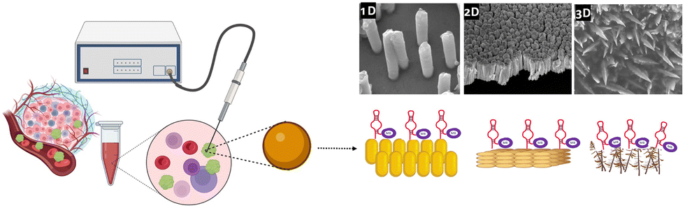 | ||
| Fig. 1 Schematic illustration of three different gold surface dimensionalities to detect MUC1, a useful prognostic biomarker for predicting cancer outcomes. | ||
To do so, bottom-up approaches were employed to synthesise one-dimensional (1D) and three-dimensional (3D) gold substrates, which later serve as substrates for the aptamer functionalization. The fabricated E-AB biosensors were then employed in the detection of the breast cancer biomarker MUC1 in human serum samples and ultimately compared with a regular gold electrode (2D) as the benchmark of the comparison.
2. Experimental
2.1. Reagents
Reagents acquired from Sigma-Aldrich were used as received unless otherwise stated: potassium hexacyanoferrate(II) trihydrate K4Fe(CN)6, human male AB plasma, USA origin, sterile-filtered, 6-mercapto-1-hexanol (C6-OH), and tris-(2-carboxyethyl) phosphine hydrochloride (TCEP). HPLC-purified and desalted anti-MUC1 DNA aptamers, HO-(CH2)6-SS-(CH2)6-O-5′-GCA GTT GAT CCT TTG GAT ACC CTG-G-3′-(CH2)7-NHCO-(CH2)3-methylene blue (MB), referred to as MB-anti-MUC1 aptamer, were used.The products were purchased from Biosearch Technologies Inc. (Novato, CA). The sequence was reported by Ferreira et al. as S1.3/S2.2.42
The 60 mer 3× VTR MUC1 peptide (PDT RPA PGS TAP PAH GVT SAP DTR PAP GST APP AHG VTS APD TRP APG STA PPA HGV TSA) was purchased from PL Laboratories Inc. (Vancouver, Canada). The peptides were suspended in a phosphate buffer (137 mM NaCl, 10 mM Na2HPO4, 1.4 mM KH2PO4, 2.7 mM KCl, pH 7.2) and stored at −20 °C.
2.2. Preparation of E-AB sensors
E-AB sensors (2D) were fabricated using a 1.6 mm diameter gold disk electrode (BAS, West Lafayette, IN). The electrode was polished with Buehler alumina slurry (1 and 0.05 μm) for 5 min, sonicated for 2 min and then transferred to a “piranha” solution (3![[thin space (1/6-em)]](https://www.rsc.org/images/entities/char_2009.gif) :1 ratio of H2SO4:H2O2) for 5 min. Finally, 25 cyclic voltammetry scans were conducted in 0.1 M H2SO4 solution from 1.4 V to 0.1 V before the electrode was incubated in 100% ethanol for another 5 min. To fabricate the E-AB sensors, the relevant aptamer solution was diluted to 0.07 μM (see below). The gold electrode was incubated in the aptamer solution for 2 h. The electrode surface was then incubated in 2 mM mercaptohexanol (MCH) for 2 h to block non-specifically adsorbed aptamers. The surface probe density (Γ) of each electrode was estimated by measuring the area under the reduction peak in cyclic voltammogram at 200 mV s−1 in 10 mM phosphate buffer saline solution (PBS) (containing 2.92 g of NaCl, 0.0690 g of NaH2PO4, and 0.071 g of Na2HPO4 plus 50 μL of 1 M MgCl2 in 25 mL of deionized water, Millipore, nanopure water, 17.5 MΩ cm−1), pH 7.2 (eqn (1)).
:1 ratio of H2SO4:H2O2) for 5 min. Finally, 25 cyclic voltammetry scans were conducted in 0.1 M H2SO4 solution from 1.4 V to 0.1 V before the electrode was incubated in 100% ethanol for another 5 min. To fabricate the E-AB sensors, the relevant aptamer solution was diluted to 0.07 μM (see below). The gold electrode was incubated in the aptamer solution for 2 h. The electrode surface was then incubated in 2 mM mercaptohexanol (MCH) for 2 h to block non-specifically adsorbed aptamers. The surface probe density (Γ) of each electrode was estimated by measuring the area under the reduction peak in cyclic voltammogram at 200 mV s−1 in 10 mM phosphate buffer saline solution (PBS) (containing 2.92 g of NaCl, 0.0690 g of NaH2PO4, and 0.071 g of Na2HPO4 plus 50 μL of 1 M MgCl2 in 25 mL of deionized water, Millipore, nanopure water, 17.5 MΩ cm−1), pH 7.2 (eqn (1)).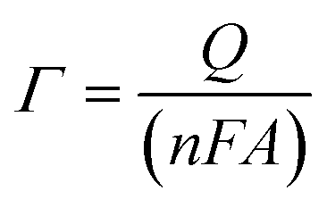 | (1) |
Electrochemical optimizations were performed in 10 mM PBS using square wave voltammetry (SWV) with an amplitude of 50 mV, a step potential of 5 mV and a frequency of 20 Hz. Electrochemical interrogations were recorded from 0.1 V to −0.5 V versus Ag/AgCl (sat. KCl) reference electrode. All other electrochemical procedures were performed in 50% diluted human serum. This 1:2 dilution was chosen not only to decrease the concentration of interfering substances that may interfere with the electrochemical measurements but also to increase the ionic conductivity allowing for better ion movement and more accurate measurements. The latter proved to display an identical signalling current to that of the PBS buffer solution.
2.3. Synthesis of gold nanostructures
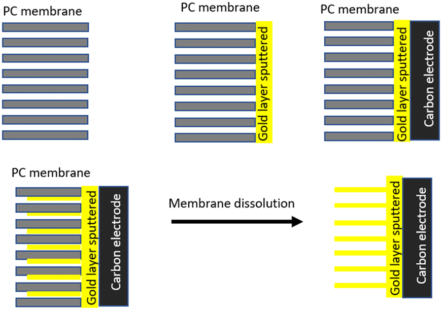 | ||
| Fig. 2 Schematic representation of template-based synthesis of gold NRs using TEPC. | ||
2.4. Physico-chemical characterization and electrochemical measurements
The surface morphology was investigated by FEI Quanta 450 environmental field-emission scanning electron microscopy (FE-ESEM), and energy-dispersive X-ray spectroscopy (EDX) was used to determine the chemical composition of the 3D gold substrate surface. Electrochemical measurements were performed using a potentiostat/galvanostat (VersaSTAT 4, Princeton Applied Research) with a three-electrode system consisting of an Ag/AgCl (sat. KCl) reference electrode, a Pt wire counter electrode, and a gold disk electrode. Electrochemical measurements were performed in 50% diluted human serum samples using SWV as described in section 2.2.Results and discussion
In this study, we investigated the influence of the gold surface dimensionality on the E-AB sensor's analytical performance in a signal-off sensor directed against the protein MUC1 in diluted human serum samples. Each sensor includes a DNA aptamer (25 nucleotides) that has been attached to the gold surface at its 5′-terminus via gold–thiol chemistry and a redox-active marker (MB) at the 3′-terminus. The E-AB sensors were built by immobilizing these modified aptamers through gold-alkanethiol chemistry on three different nanostructured gold surfaces: control 2D, 3D NS, and 1D NR. Fig. 3A–C show the scanning electron micrographs of the top view of a representative TEPC membrane (A) and the corresponding Au NR electrode after the removal of the TEPC membrane (B and C).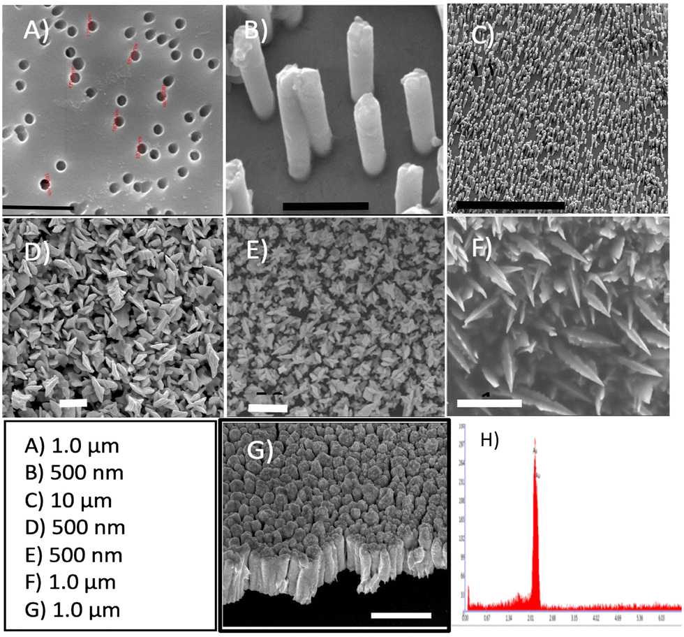 | ||
| Fig. 3 Scanning electron micrographs of the gold substrates: A) surface of the TEPC membrane, B) close view of the 1D NR, C) the electrode surface with a 1D orientation, D) zoomed-in top-view of the 3D NS, E) zoomed-out top-view of the 3D NS, F) tilted view of the 3D NS, G) side-view of the 2D gold surface, and H) EDX spectrum from the 3D gold NS. | ||
The electrode surface is fully covered by high-density (∼5.0 × 10⁸ NR cm−2) and parallel NRs of 200 nm in diameter and 800 nm in length, with an inter-distance of 300 nm to 700 nm between them (Fig. 3B and C).
In Fig. 3D and E, the surface of the electrode exhibits a uniform coating of well-defined Au NSs with prismatic tapering ends. The top view of 3D gold NSs indicates a base thickness dimension of about ∼350 nm (Fig. 3E and F) and approximately 500 nm in length. Lastly, in Fig. 3G one can see the side-view of the 2D sputtered-gold surface. Complete removal of Pb for the NS structure has been confirmed with EDX analysis as shown in Fig. 3H. Fig. 4A shows the cyclic voltammograms obtained at each Au surface. The evolution of larger peaks (both oxidation and reduction) for NS and NR (black and blue curves) vs. 2D gold surface (red curve) account for the contribution of the higher surface area of the corresponding Au NS and Au NR nanostructures. Also, it is evident that, compared to the Au 2D electrode (red curve), the other two counterparts (black and blue curves) have shown 0.05 V reduction in the peak-to-peak separation (ΔE = Epa − Epc). It has been demonstrated that the higher surface area and evolution of higher degree of edge effect are key factors to address these effects.44,45
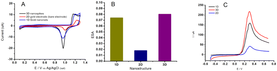 | ||
| Fig. 4 A) CV curves of a gold electrode featuring various morphological aspects of 1D, 2D, and 3D nanostructures. Cyclic voltammetry was performed in 0.1 H2SO4 solution with a sweep rate of 0.05 V s−1. B) The ECSA comparison. C) The corresponding LSV curves obtained in water solution containing K4Fe(CN)6 (10.0 mM), ν = 0.1 V s−1. | ||
The electrochemical active surface area (ECSA) of the Au control, Au NSs and Au NRs were determined using cyclic voltammetry in 0.1 M H2SO4 solution. The area under the reductive cathodic peak (background current excluded) on the voltammogram is proportional to the real surface area (ECSA = Q/390 uC cm−2) and is therefore an indication of surface roughness.
ECSA was calculated from the cathodic peak which is related to the removal of the monolayer of oxide formed on the surfaces during the onward scan of cyclic voltammetry. As expected, the ECSA of the Au NSs (0.079 cm2) and NRs (0.072 cm2) revealed significant enhancement compared to that of the control Au electrode (0.02 cm2), as shown in Fig. 4B. Fig. 4C demonstrates the effect of surface area enhancement on the corresponding electrochemical activity. Given the geometrical area of the Au 2D electrode ca., 0.02 cm2, roughness factors (Rf, the ratio of ECSA to geometrical area) of 3.95 and 3.6 were calculated for the NS and NR, respectively. This evidence, the apparent roughness value enhancement, will account for the successful preparation of gold nanostructures on the electrodes.
Given the E-AB sensor's signalling mechanism,46 in which detection is achieved by relying on binding induced changes in the electron transfer rate between a surface-bound, reporter-modified aptamer and an electrode, the electron transfer rate before and after MUC1 hybridization at the electrode surface is dependent on the SWV frequency used to interrogate the electrode, as well as the packing density of the aptamers. The latter was optimized by measuring the signal response of MUC1 on the aptamer-modified gold electrode using various concentrations of the probe aptamer. An optimal probe density was achieved at 4.7 × 10¹² molecule per cm−2, corresponding to an aptamer solution of 70 nM. Due to the size of surface nanostructures (>60 nm),47 a similar probe surface density of 4.7 × 10¹² molecule per cm−2 is expected for 1D and 3D based E-AB sensors.48 Given that they will share the same probe surface density, the difference in performance will be only the result of surface dimensionality.
Au nanostructures can influence the kinetics of hybridization by interfering with the target diffusion, target/probe interaction and aptamer conformational changes. Fig. 5 reveals whether micro- and macrostructural features of the three nanostructures will influence the sensitivity and thus the aptamer's performance. The kinetics of hybridization (response time) vs. gain for the three electrodes were monitored and compared. Here the response time is used as a measure for identifying the kinetics of hybridization.49
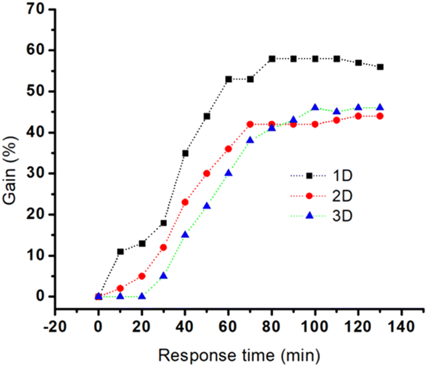 | ||
| Fig. 5 Representation of the typical response time (signal suppression) of the various E-AB sensors featuring 1D, 2D, and 3D gold substrates during 2 h incubation with a saturated concentration of MUC1 in 50% diluted human serum. Data points have been collected from a single measurement. | ||
A steep hybridization curve demonstrates a better affinity and accessibility of the target to the probe. The results are displayed in Fig. 5, and their response time vs. signal gain (defined as the ratio of the current change at a given target concentration and the initial current) were compared. The results show that the electrodes exhibited a similar behaviour in terms of gain variations vs. time (hybridization kinetic) until a plateau is reached. The highest gain (∼60%) was achieved for Au NR (1D) electrodes in 70 minutes whereas Au NS (3D) and Au control (2D) required 70 minutes to reach a gain of 40%. These gain variations, in the case of Au NR (1D), started to be measurable only after 10 min in contact with MUC1, whereas Au Ns (3D) and the control electrodes (2D) needed at least 20–30 min. This hybridization kinetic behaviour is likely due to the difference between accumulation of MUC1 on the sensor surface and can be easily influenced by the surface geometry-induced steric hindrances.50 The influence of Au dimensionalities on the analytical performance of the corresponding E-AB sensors was analysed with increased concentrations from 0 nM to 650 nM of MUC1 in the 50% diluted human serum samples. The corresponding signal changes (Δi is the change of peak current before and after addition of MUC1) were monitored via an SWV technique (Fig. 6A–C). The SWV voltammograms showed a proportional decrease of MB current at ∼−0.25 V vs. Ag/AgCl with the increase of MUC1 concentrations.
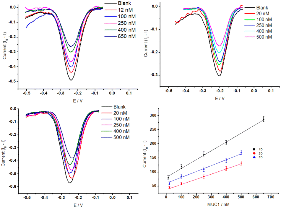 | ||
| Fig. 6 SWV responses of the E-AB sensors featuring 1D (A), 2D (B), and 3D (C) gold substrates after incubating with MUC1 at different concentrations. (D) Collected calibration lines for the detection of MUC1 based on various dimensionalities. The experiment was carried out with an amplitude of 50 mV, a step of 5 mV, and a frequency of 20 Hz in the 50% diluted human serum samples. | ||
The SWV data were converted into a calibration plot by plotting the signal suppression vs. concentration of MUC1 (Fig. 6D).
MB redox peak linearly decreased in response to the addition of MUC1 for the three electrodes. We obtained the corresponding regression equation of Δi = (0.33 ± 0.03)x + (81.51 ± 9.9) (R2 = 99.47, N = 5), Δi = (0.18 ± 0.03)x + (37.72 ± 7.6) (R2 = 99.30, N = 5), and Δi = (0.20 ± 0.03)x + (60.56 ± 7.6) (R2 = 98.82, N = 5), for NRs (1D), control (2D) and NSs (3D) featuring E-AB sensors (based on 95% confidence interval, t(n−2) = 3.18).51 A limit of detection (LOD) (calculated by 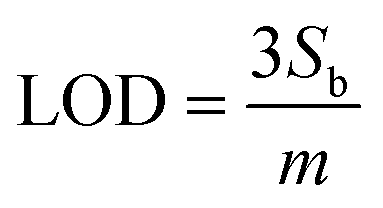 , where Sb is the standard deviation of the blank measures and m is the slope of the calibration plot obtained from the linear regression analysis) of 3.5 nM, 7.8 nM, and 6.8 nM was correspondingly estimated for NRs (1D), 2D control, and NSs (3D) featuring E-AB sensors. The lowest Au dimension appears to provide the best sensitivity as well as, a wider LDR from 12 nM to 650 nM, compared to 3D NS and Au 2D electrodes that exhibit an LDR between 20 nM to 500 nM. The observed behaviour can be most likely explained through the influence of the surface morphology on the surface organization of aptamers. The large surface area of the 1D gold substrate (0.072 cm2), compared to the gold 2D substrate (0.02 cm2) significantly increased the immobilization sites for the MUC1 probe aptamers. Despite exhibiting a higher surface area, 3D Au NS did not perform as well as 1D Au NS. This discrepancy between the surface area and electrochemical performances can be caused by the orientation of aptamers which vary strongly with the surface chemistry and morphology of the substrate. It has been shown that gold nanorods have a more uniform surface morphology and surface charge distribution, which allows for better alignment and immobilization of the aptamers on the surface. In contrast, gold nanospikes and gold layers have more irregular surface features, such as sharp edges and rough surfaces, which can disrupt the alignment of the aptamers and result in less consistent orientation. Additionally, the binding affinity of the aptamer for the substrate can also play a role in the orientation of the aptamer. If the aptamer has a stronger affinity to one surface compared to another, it may be more likely to align properly on that surface. Therefore, while the exact reason on the effect of surface area on the signal gain, which is offset in the 3D structure, is not entirely clear, irregular surface features, sharp edges and weaker binding affinity are believed to lead to unproper alignment of aptamers on that surface, and additionally the nanospike morphology might also be unfavourable for the conformational change after target hybridization.
To investigate the repeatability, we prepared three fresh E-AB sensors and incubated them with saturated concentration of MUC1 in 50% human serum samples (Fig. 7).
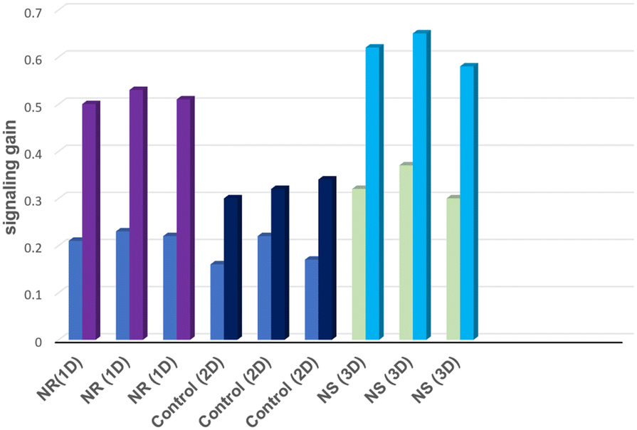 | ||
| Fig. 7 Shows repeatability results for three freshly prepared E-AB sensors 1D, 2D, and 3D. The left bar represents the initial signal of the E-AB sensor, and the right bar is the signal gain after target hybridization. | ||
All E-AB sensors exhibited similar signalling behaviours with relative standard deviations (RSD) of 4.1% (NR), 4.5% (control), and 3.7% (NS), respectively. These values demonstrate that the repeatability character of the E-AB sensors within the corresponding time frame (90 min) was satisfactory. Moreover, the stability of the fabricated E-AB sensors was also examined. Following the storage in the refrigerator at 4 °C for 9 days, NR (1D) and NS (3D) based aptasensors retained 91% and 95% of their initial currents, respectively, whereas the control electrode (2D) lost more than 90% of its initial value after only 3 days. The stabilization of aptamers via nanostructures is a well-documented effect.40,41 Nanostructure employment can increase the robustness of the surface which leads to higher stability of surface immobilization.
Conclusions
In this work, the surface nano-dimensionality and the corresponding influence on the E-AB sensor performance were investigated. Two bottom-up approaches, a template-based synthesis using TEPC and electrochemical deposition, were used to build and synthesize 1D gold NRs (ECSA = 0.072 cm2) and 3D gold NSs (ECSA = 0.079 cm2), respectively. After attachment of aptamers on the various Au surfaces using gold-thiol chemistry, the analytical performances were measured and compared to the regular gold electrode (ECSA = 0.02 cm2) as the benchmark of the study. The lowest LOD was obtained for the 1D NR with 3.5 nM versus 6.8 nM for the 3D NS featuring electrode, compared to 7.8 nM estimated using the control E-AB sensor. Our data revealed that, contrary to the general perception, increasing the surface area not always leads to a higher gain if there is a morphological counterplay. Also, the data suggested that the surface/orientation of aptamers, on top of the alkanethiols SAM, may strongly rely on the surface morphology features and eventually affects the sensor performance/sensitivity. But the surface enhancement on the electrode due to the application of NS and NR demonstrated a significant improvement in the shelf-life of the E-AB sensors (∼9 days) relative to the control sensor with a planar surface (∼3 days). Studying various aptamer lengths on the nanoscale surface is required to confirm its effect on sensor performance, including aptamer's surface organization and target-probe dynamics.Author contributions
Conceptualization, AK and G. M.; methodology, A. K.; validation, AK; formal analysis, AK; resources, G. M.; data curation, AK; writing—original draft preparation, A. K.; writing—review and editing, E. H. and G. M.; supervision, G. M.; funding acquisition, G. M. All authors have read and agreed to the published version of the manuscript.Conflicts of interest
There are no conflicts to declare.Acknowledgements
This research was funded by NSERC discovery grant (RGPIN-2020-05884) and FRQS chercheur boursier J1 (266388).References
- N. S. Que-Gewirth and B. A. Sullenger, Gene Ther., 2007, 14, 283–291 CrossRef CAS PubMed.
- S. Song, L. Wang, J. Li, C. Fan and J. Zhao, TrAC, Trends Anal. Chem., 2008, 27, 108–117 CrossRef CAS.
- C. M. Dollins, S. Nair and B. A. Sullenger, Hum. Gene Ther., 2008, 19, 443–450 CrossRef CAS PubMed , https://home.liebertpub.com/hum.
- Y. Xiao, R. Y. Lai and K. W. Plaxco, Nat. Protoc., 2007, 2, 2875–2880 CrossRef CAS PubMed.
- M. Sharafeldin and J. J. Davis, Anal. Chim. Acta, 2022, 1216, 339759 CrossRef CAS PubMed.
- J. Muñoz, R. Montes and M. Baeza, TrAC, Trends Anal. Chem., 2017, 97, 201–215 CrossRef.
- D. Bizzotto, I. J. Burgess, T. Doneux, T. Sagara and H. Z. Yu, ACS Sens., 2018, 3, 5–12 CrossRef CAS PubMed.
- J. J. Gooding and N. Darwish, Chem. Rec., 2012, 12, 92–105 CrossRef CAS PubMed.
- Y. Xiao, T. Uzawa, R. J. White, D. DeMartini and K. W. Plaxco, Electroanalysis, 2009, 21, 1267–1271 CrossRef CAS PubMed.
- T. Cholko and C. E. A. Chang, J. Phys. Chem. B, 2021, 125, 1746–1754 CrossRef CAS PubMed.
- M. Lin, J. Wang, G. Zhou, J. Wang, N. Wu, J. Lu, J. Gao, X. Chen, J. Shi, X. Zuo and C. Fan, Angew. Chem., 2015, 127, 2179–2183 CrossRef.
- A. L. Furst, M. G. Hill and J. K. Barton, Langmuir, 2013, 29, 16141–16149 CrossRef CAS PubMed.
- A. B. Steel, R. L. Levicky, T. M. Herne and M. J. Tarlov, Biophys. J., 2000, 79, 975–981 CrossRef CAS PubMed.
- T. M. Herne and M. J. Tarlov, J. Am. Chem. Soc., 1997, 119, 8916–8920 CrossRef CAS.
- F. Ricci, R. Y. Lai, A. J. Heeger, K. W. Plaxco and J. J. Sumner, Langmuir, 2007, 23, 6827–6834 CrossRef CAS PubMed.
- F. Ricci, N. Zari, F. Caprio, S. Recine, A. Amine, D. Moscone, G. Palleschi and K. W. Plaxco, Bioelectrochemistry, 2009, 76, 208–213 CrossRef CAS PubMed.
- M. D. Mayer and R. Y. Lai, Talanta, 2018, 189, 585–591 CrossRef CAS PubMed.
- C. Y. Lee, P. Gong, G. M. Harbers, D. W. Grainger, D. G. Castner and L. J. Gamble, Anal. Chem., 2006, 78, 3316–3325 CrossRef CAS PubMed.
- K. K. Leung, A. D. Gaxiola, H. Z. Yu and D. Bizzotto, Electrochim. Acta, 2018, 261, 188–197 CrossRef CAS.
- N. Dimcheva, Curr. Opin. Electrochem., 2020, 19, 35–41 CrossRef CAS.
- K. Urmann, J. Modrejewski, T. Scheper and J. G. Walter, BioNanoMaterials, 2016 DOI:10.1515/BNM-2016-0012.
- M. Shariati, M. Ghorbani, P. Sasanpour and A. Karimizefreh, Anal. Chim. Acta, 2019, 1048, 31–41 CrossRef CAS PubMed.
- F. Tulli, F. A. Gulotta, D. M. Martino, V. I. P. Zanini and C. D. Borsarelli, J. Electrochem. Soc., 2018, 165, B452–B457 CrossRef CAS.
- N. Kumar and S. Kumbhat, Essentials in Nanoscience and Nanotechnology, 2016, pp. 326–360 Search PubMed.
- P. N. Navya and H. K. Daima, Nano Convergence, 2016, 3, 1 CrossRef CAS PubMed.
- P. R. Solanki, A. Kaushik, V. V. Agrawal and B. D. Malhotra, NPG Asia Mater., 2011, 3, 17–24 CrossRef.
- Q. Zhou and T. Kim, Sens. Actuators, B, 2016, 227, 504–514 CrossRef CAS.
- L. Soleymani, Z. Fang, E. H. Sargent and S. O. Kelley, Nat. Nanotechnol., 2009, 4, 844–848 CrossRef CAS PubMed.
- P. E. Sheehan and L. J. Whitman, Nano Lett., 2005, 5, 803–807 CrossRef CAS PubMed.
- I. Hammami, N. M. Alabdallah, A. Al Jomaa and M. Kamoun, J. King Saud Univ., Sci., 2021, 33(7) DOI:10.1016/J.JKSUS.2021.101560.
- Z. Yan, M. G. Taylor, A. Mascareno and G. Mpourmpakis, Nano Lett., 2018, 18, 2696–2704 CrossRef CAS PubMed.
- M. G. Taylor, N. Austin, C. E. Gounaris and G. Mpourmpakis, ACS Catal., 2015, 5, 6296–6301 CrossRef CAS.
- K. M. Bratlie, H. Lee, K. Komvopoulos, P. Yang and G. A. Somorjai, Nano Lett., 2007, 7, 3097–3101 CrossRef CAS PubMed.
- M. Arenz, U. Landman and U. Heiz, ChemPhysChem, 2006, 7, 1871–1879 CrossRef CAS PubMed.
- X. J. Huang, A. M. O'Mahony and R. G. Compton, Small, 2009, 5, 776–788 CrossRef CAS PubMed.
- A. Walcarius, S. D. Minteer, J. Wang, Y. Lin and A. Merkoçi, J. Mater. Chem. B, 2013, 1, 4878–4908 RSC.
- L. Shi, Z. Chu, X. Dong, W. Jin and E. Dempsey, Nanoscale, 2013, 5, 10219–10225 RSC.
- A. M. Downs, J. Gerson, M. N. Hossain, K. Ploense, M. Pham, H. B. Kraatz, T. Kippin and K. W. Plaxco, ACS Sens., 2021, 6, 2299–2306 CrossRef CAS PubMed.
- N. Arroyo-Currás, K. Scida, K. L. Ploense, T. E. Kippin and K. W. Plaxco, Anal. Chem., 2017, 89, 12185–12191 CrossRef PubMed.
- X. Bin, E. H. Sargent and S. O. Kelley, Anal. Chem., 2010, 82, 5928–5931 CrossRef CAS PubMed.
- S. Ranjbar, S. Shahrokhian and F. Nurmohammadi, Sens. Actuators, B, 2018, 255, 1536–1544 CrossRef CAS.
- C. S. M. Ferreira, C. S. Matthews and S. Missailidis, Tumor Biol., 2006, 27, 289–301 CrossRef CAS PubMed.
- B. Plowman, S. J. Ippolito, V. Bansal, Y. M. Sabri, A. P. O'Mullane and S. K. Bhargava, Chem. Commun., 2009, 5039–5041 RSC.
- Q. Cao, Z. Shao, D. K. Hensley, N. V. Lavrik and B. J. Venton, Langmuir, 2021, 37, 2667–2676 CrossRef CAS PubMed.
- D. W. M. Arrigan, Analyst, 2004, 129, 1157–1165 RSC.
- A. A. Lubin and K. W. Plaxco, Acc. Chem. Res., 2010, 43, 496–505 CrossRef CAS PubMed.
- H. D. Hill, J. E. Millstone, M. J. Banholzer and C. A. Mirkin, ACS Nano, 2009, 3, 418–424 CrossRef CAS PubMed.
- H. D. Hill, J. E. Millstone, M. J. Banholzer and C. A. Mirkin, ACS Nano, 2009, 3, 418–424 CrossRef CAS PubMed.
- A. A. Lubin, B. V. S. Hunt, R. J. White and K. W. Plaxco, Anal. Chem., 2009, 81, 2150–2158 CrossRef CAS PubMed.
- S. S. Mahshid, S. Camiré, F. Ricci and A. Vallée-Bélisle, J. Am. Chem. Soc., 2015, 137, 15596–15599 CrossRef CAS PubMed.
- J. N. Miller, J. C. Miller and R. D. Miller, Statistics for Analytical Chemistry, Pearson Education, England, 4th edn, 2000, ch. 7, p. 292 Search PubMed.
| This journal is © The Royal Society of Chemistry 2023 |