
 Open Access Article
 This Open Access Article is licensed under a
 Creative Commons Attribution 3.0 Unported Licence
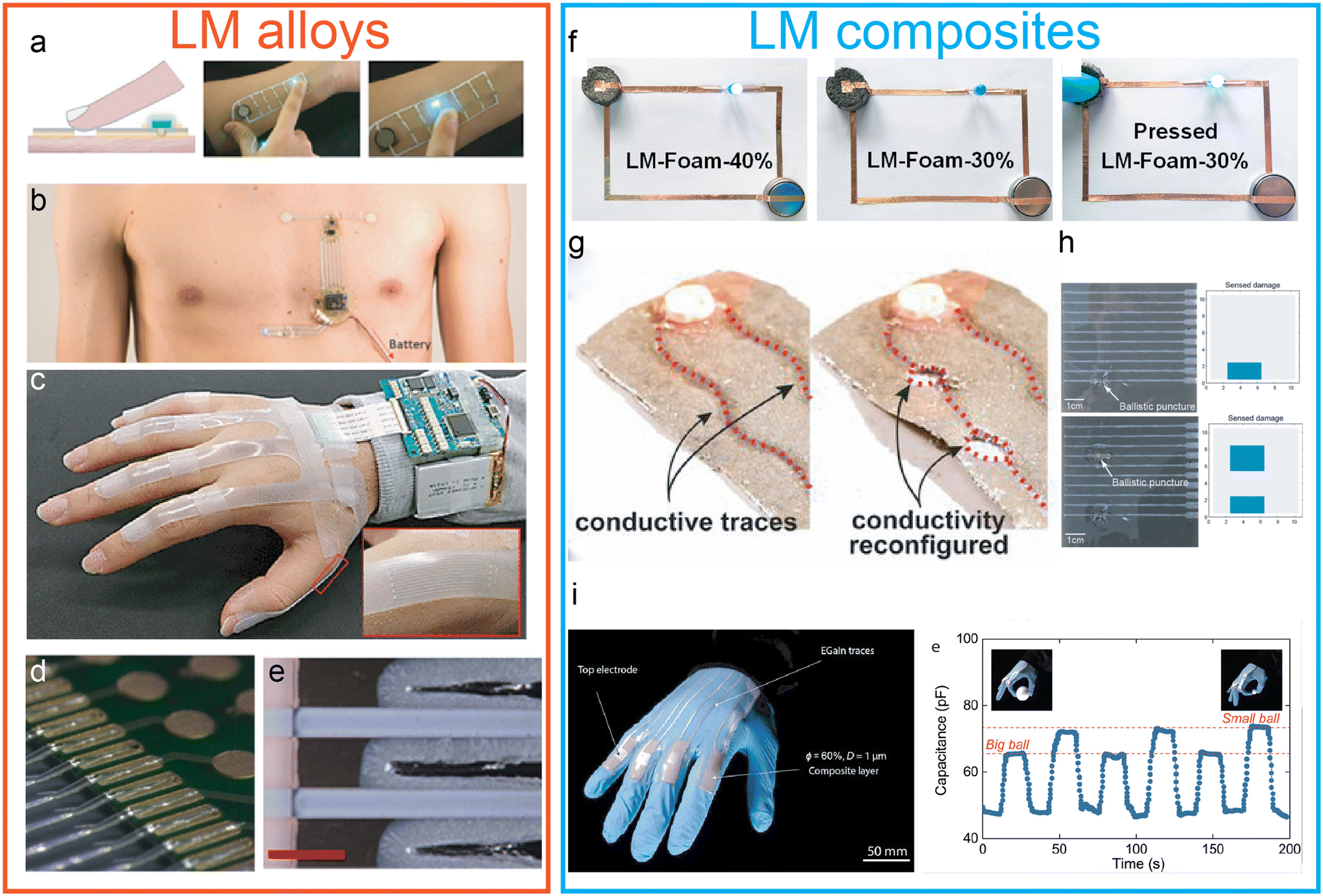
Biphasic liquid metal mixtures in stretchable and flexible applications
Nyamjargal
Ochirkhuyag
 ,
Yuji
Isano
,
Kota
Inoue
and
Hiroki
Ota
*
,
Yuji
Isano
,
Kota
Inoue
and
Hiroki
Ota
*
Yokohama National University, 79-5 Tokiwadai, Hodogaya-ku, Yokohama, 240-8501 Japan. E-mail: ota-hiroki-xm@ynu.ac.jp
First published on 17th February 2023
Abstract
Liquid metals (LMs) have emerged as key materials for soft and wearable electronics owing to their unique properties such as fluidity, deformability, low toxicity, high electrical and thermal conductivities, self-healing, and biocompatibility. Moreover, LMs can be mixed with other metal particles and soft materials to form two-phase structures. Wearable and stretchable electronic devices can utilize biphasic LM mixtures as a material with different characteristics from those of conventional LMs. Biphasic LM mixtures consist of solid and liquid phases which are defined, respectively, as LM with solid metal particles and LM inside a soft material. An LM with solid metal particles consists of an alloy of LM and a metal such as Ni or Cu. In contrast, an LM with a soft material is composed of LM and an elastomer such as polydimethylsiloxane (PDMS) or Ecoflex. Sensors and field-effect transistors (FETs) utilizing two-phase LM mixtures are discussed in this paper. Additionally, fabrication and patterning of two-phase LM mixtures are discussed.
 Nyamjargal Ochirkhuyag | Nyamjargal Ochirkhuyag is a PhD student in the Department of Mechanical Engineering, Yokohama National University (YNU), Japan, in Prof Hiroki Ota's research group. She obtained her MEng in Nanoscience and Nanoengineering at New Mongol Institute of Technology (NMIT), Mongolia in 2019 and her BEng in Electronic engineering with Nanotechnology at Swansea University, UK in 2016. She has been working on liquid metal based stretchable electric applications. |
 Yuji Isano | Yuji Isano is a master's student in the Department of Mechanical Engineering, Yokohama National University (YNU), Japan, in Prof Hiroki Ota's research group. He received his B.E. degree in Mechanical Engineering at YNU in 2021. His research interest is focused on the development of integrated systems of stretchable devices and machine learning. |
 Kota Inoue | Kota Inoue is a master's student in the Department of Mechanical Engineering at Yokohama National University (YNU), Japan, in Prof. Hiroki Ota's research group. He received his B.E. degree in Mechanical Engineering at Yokohama National University in 2022. His research interests focus on sensors based on FET devices. |
 Hiroki Ota | Hiroki Ota is an Associate Professor in the Department of Mechanics, Yokohama National University (YNU), Japan. He received his B.S. and M.S. in Applied Physics, and PhD in Mechanics at Keio University, Japan in 2005, 2007, and 2011, respectively. He joined Canon Inc. as an engineer of a printer (2007-2008). He was a post doctor in Joint Institution of Tokyo Women's Medical University-Waseda University for Advanced Biomedical Sciences and Department of Electrical Engineering in University of California, Berkeley, USA, until 2016, and an assistant professor in the Department of Applied physics, Osaka University, Japan until February 2017. His current research at YNU is the development of flexible sensors/actuators using liquid metal and smart devices for healthcare. |
Introduction
Flexible and stretchable electronics constitute a novel technology with potential applications in fields such as monitoring, sensing, and medical devices.1,2 In wearable and soft electronic devices, various flexible soft polymers, such as polydimethylsiloxane (PDMS), Ecoflex, silicone, polyurethane, polyimide, parylene, and polymethyl methacrylate, have been proposed as substrate materials,3–5 exhibiting durability and biocompatibility. Conductive materials, however, must be improved for electrodes. Conductive materials such as carbon,6 graphene,7 and metallic materials8 have been proposed for large-deformation devices. However, the disadvantage of conductive materials is the large variation in resistance or plastic deformation caused by large deformations. Therefore, LMs are attracting attention as materials with physical and electrical stabilities against deformation for next-generation highly deformable electrodes.Liquid metals (LMs), which possess a unique combination of fluidic and metallic properties, such as liquid state at or below room temperature and high thermal and electrical conductivities, have been used for various applications, such as soft electronics, drug delivery, microfluidics, and energy harvesting devices. In stretchable and flexible electronic devices, LMs have received significant attention owing to their low viscosity, high stretchability, self-healing capability, excellent conductivity, easy modifications, and reconfigurability.9–11 Moreover, a thin oxide skin of approximately 3 nm can be formed on the surface of LM under ambient conditions, allowing LM to adhere to surfaces and adopt shapes that are useful for soft, flexible, and stretchable electronics.12 With its chemical, physical, and metallic properties, LM is a promising material for development of soft and multifunctional wearable sensors with excellent stretchability and sensitivity. Furthermore, LMs are used not only as materials but also as flexible wirings and interconnections.13,14 Additionally, LMs provide good electrical contacts in complex morphologies and three-dimensional substrates along with deformability for field-effect transistors (FETs), which are generally used as signal amplifiers in wearable sensors.15,16
As LMs have been gaining attention in soft and reconfigurable electronics applications, LM mixtures with other metals and elastomers are being developed to enhance their capabilities and properties when biphasic LM mixtures are created. Biphasic LM mixtures, which are discussed in this review article, can be defined as “LMs with solid metal particles inside and LM composites where LM is inside elastomers”. Solid metal particles of biphasic LM can be micro or nanoscale in size. The advantages of biphasic LM mixtures are their high conductivity, excellent stretchability, and good adhesion to various substrates.17 Gallium-based LMs can be easily alloyed with other metals, such as indium, tin, copper, iron, nickel, bismuth, cadmium, and lead with tuneable melting points by incorporating different compositions and proportions. When alloying with other metals, the oxide skin of LM affects the adjustment of its shape. An LM alloy with other metals can have high adhesive behaviour, and it can enhance electrical and thermal conductivities, transformable capability, and excellent flexibility.18,19 Moreover, LM and polymer composites can exhibit both properties: high conductivity of LM and shape-morphing capability of polymers. The LM–PU (polyurethane) composite exhibits a bilayer structure and achieves excellent shape-morphing abilities due to the phase transitions of LM and crystalline PU elastomers.20
Biphasic liquid metal mixtures and their applications in flexible and stretchable electronics are highlighted in this article. Additionally, the properties and tuning methods of LM alloys (biphasic LM mixture with solid metal particles) and composites (biphasic LM mixture with elastomers) with organic materials and patterning techniques for circuit fabrication are summarized. In addition, we focus on the development of flexible and stretchable sensors and FETs based on the basic properties and technologies of these materials. This development is crucial for the integration and complexity of flexible and stretchable electronics for social implementation, and this review contributes to their development.
Biphasic LM mixtures
An LM is known as a single element or alloy with a low melting point, and it has a liquid phase at a temperature equal to or lower than the room temperature. The most representative LM is gallium (Ga), which is known as low toxicity and has a melting point of 303 K. The melting point of an alloy depends on compositions, for example, for gallium–indium (Ga–In), gallium–tin (Ga–Sn), and gallium–indium–tin (Ga–In–Sn) alloys, melting points are 288.3, 293.7, and 278–283.7 K, respectively. EGaln, galinstan, and Ga–Sn alloys are familiar LM alloys. EGaln consists of 75.5% Ga and 24.5% In; galinstan consists of 68.5% Ga 21.5% In and 10% Sn; and Ga–Sn alloy consists of 88% Ga and 12% Sn. An LM is synthesized by melting and mixing metals in a vial on a hot plate. The addition of metals to LMs can improve either the properties of LM or additives. Moreover, when LM alloys with copper (Cu), silver (Ag), gold (Au), and carbon nanotubes (CNTs) are used, the thermal conductivity of the LMs are enhanced. In contrast, LMs alloyed with iron (Fe) or nickel (Ni) exhibit magnetic properties. Moreover, when LM is composited with elastomers, it not only improves the thermal and electrical conductivities of LM, but also enhances the toughness of elastomers.21,22Fig. 1 illustrates the fabrication and patterning of LM mixtures for stretchable and flexible sensors and FET applications.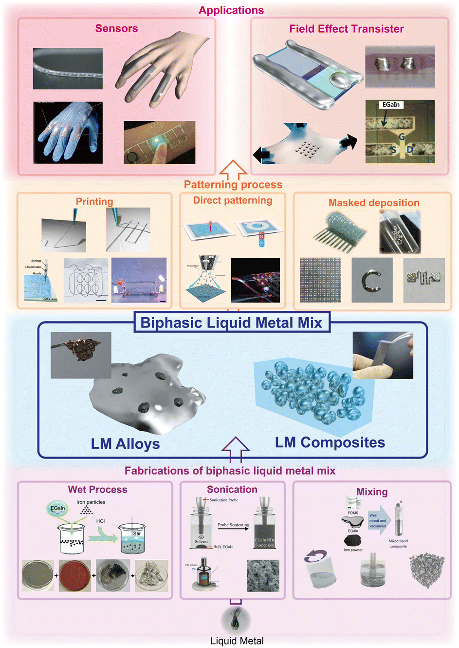 | ||
| Fig. 1 Biphasic LM mixtures toward stretchable and flexible applications. | ||
Sensors are core devices for acquiring information as they can detect external stimuli and transform them into measurable signals. Flexible and wearable sensors have been developed, and they have shown advantages, especially in biomedical applications such as health monitoring and intelligent robotics.13 Mechanical sensors that respond to external forces in the form of pressure, strain, and torque, should be flexible, stretchable, durable, and sensitive since their operation is based on changes in mechanical stimuli. Additionally, LMs make them deformable, responsive, durable, and self-healing.14
Flexible FETs are potential sensing devices owing to the variety of material utilization and self-amplifying function on electrical signals. Thus, they have demonstrated the ability to detect different types of external stimuli and continuous monitoring functionalities.23 Furthermore, FET-based sensors exhibit higher sensitivity than sensors owing to their signal amplification capability by controlling the voltage applied to the gate electrode.24
Liquid metal alloys with solid metal particles
Galinstan and EGaln are generally used as interconnections in electronic applications owing to their high electrical conductivities. Ga alloy with other metals can be fabricated by placing the appropriate quantities of metals in a container, and heating and mixing are performed to obtain a proper blend.25 Different methods can be used to fabricate LM alloys with other metals. The porous LM foam is fabricated by mixing EGaln and Fe particles, which have both metal and flexibility properties, as shown in Fig. 2a. EGaln and Fe particles were stirred in a beaker with hydrochloric acid (HCI), which was added to remove the oxide layer on surface of the mixture to enhance the absorption of Fe particles by LM. When Fe particles were appropriately absorbed in LM, a permanent magnet was placed outside the beaker to enhance the concentration of Fe particles in a specific volume of the LM bulk. This enrichment process enabled higher viscosity and stronger magnetism.26 In contrast, galinstan with Cu particles can be fabricated by the oxide-free ultrasonication-assisted particle internalization method (Fig. 2b–f) that dispersed copper nanoparticles (Cu-NPs) into galinstan and formed crosslinking structures for thermal percolation. The thermal conductivity of this alloy was 64.8 Wm−1 K−1 at 4 vol%, which was approximately 180% higher than that of untreated galinstan.27 Thus, transitional state metallic mixtures composed of Ga–In alloy with Cu particles were prepared by two-stage route (Fig. 2g). The first stage involved an electrical polarization-assisted particle internalization process performed in NaOH solution to remove the oxide layer on the LM and Cu particles using an external voltage of 5 V. The wet-processing stage involved the introduction of water and particles to the LM for the intermediate product. The second stage involved vacuum drying to exhaust water content immediately after the first stage.28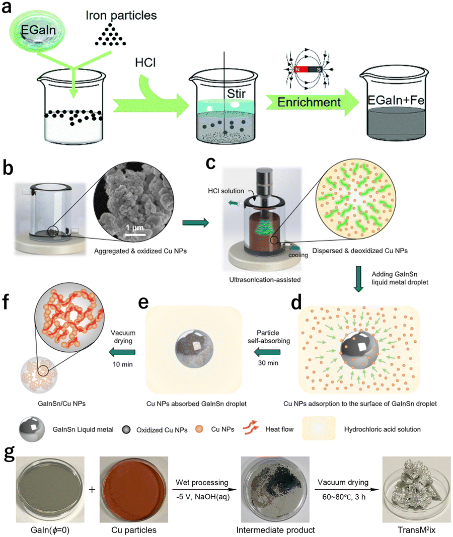 | ||
| Fig. 2 Synthesis of LM alloys with solid metal particles. (a) Fabrication process of porous LM foams. Reproduced from ref. 26 with permission from Royal Society of Chemistry (RSC), copyright 2017. (b)–(f) Fabrication process of oxide-free ultrasonication-assisted particle internalization method. Reproduced from ref. 27 with permission from Elsevier, copyright 2021. (g) Two-stage route fabrication process. Reproduced from ref. 28 with permission from American Chemical Society (ACS), copyright 2017. | ||
Moreover, Chang et al. (2018) presented a method to fabricate a sticky LM with good plasticity, called GIN. EGaln and nickel (Ni) powder were placed in a beaker and stirred continuously at the room temperature for 10 min. Subsequently, two layers of liquid were observed in the beaker: the upper layer was viscous and less shiny, while the lower layer was not different from EGaln. Afterward, it was placed in the open for 10 h. Furthermore, the upper layer became sticky and lacklustre, known GIN material. This material can be easily patterned, and they exhibit excellent adhesion to printer paper, and provide stable and flexible electrical connections.29
Liquid metal composition with soft elastomers
Liquid metal composites with soft elastomers can be fabricated by shear mixing and polymerization or surface-initiated atom transfer.30 Shear mixing method was used to create different-sized LM particles dispersed in elastomers, such as PDMS and Ecoflex. Thus, composites of EGaln and Ecoflex-0030 are fabricated by combining the mixing and probe sonication methods, as shown in Fig. 3a. The size of the LM droplets was tuneable during fabrication. Composite fabrication can be performed in the following three steps. 1. Combine the LM droplets in the uncured and liquid elastomers, 2. To obtain an LM particle of size <5 μm, probe sonication with shear mixer was used in combination, 3. Add the elastomer again to dilute the emulsion to obtained the required LM volume loading, and use shear mixer to homogenize and degas.31 Polymerization method involves the formation of a highly cross-linked particle-polymer network on the oxide layer of LM. Polymerized LM networks (poly-LMNs) are fabricated based on EGaln, as shown in Fig. 3b. Immediately after fabrication, these networks exhibited unmeasurable conductivity because the particles were isolated by their oxide shells/oxide skins. However, poly-LMNs were ruptured, and metal cores were released to flow when stretched uniaxially. At this point, poly-LMNs were activated, resulting in a rapid 108-fold increase in network conductivity.32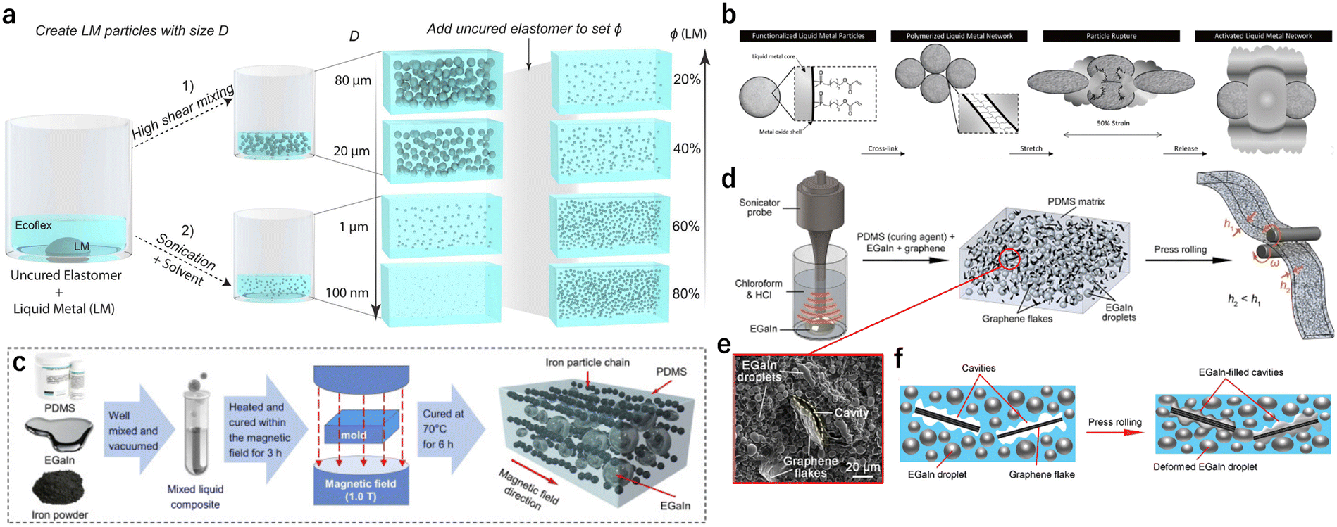 | ||
| Fig. 3 Fabrication of LM embedded in elastomers. (a) Combination of shear mixing and ultra-sonication methods. Reproduced from ref. 31 with permission from ACS, copyright 2019. (b) Polymerization method. Reproduced from ref. 32 with permission from Wiley & Sons, copyright 2019. (c) Fabrication of LM embedded elastomer with magnetic property. Reproduced from ref. 34 with permission from Elsevier, copyright 2020. (d)–(f) Combining LM in elastomer with addition of graphene flakes. Reproduced from ref. 35 with permission from Wiley & Sons, copyright 2019. | ||
The advantage of combining LM with elastomers is that they are highly deformable materials that retain the properties of LM alloys. To create a soft elastomer with magnetic properties, an LM alloy with magnetic metals was embedded in the elastomer. The LM-filled magnetorheological and deformable elastomer is fabricated by mixing and stirring EGaln with Fe particles in uncured PDMS at high speed and then vacuumed to remove air bubbles, as shown in Fig. 3c. The composite showed unique properties, such as a positive piezo-conductive effect, where the resistivity was maximized in the relaxed state and dropped dramatically in mechanical deformations. Thus, the magnetic field response reduced its resistivity in magnetic field.33,34 To achieve a highly electrically conductive and flexible elastomer, EGaln was embedded in PDMS with the addition of graphene flakes. Furthermore, LM micro-nano droplets are synthesized in a chloroform–HCI mixture with continuous N2 purging and mixed with PDMS, as depicted in Fig. 3d. Chloroform was used as a solvent because it can be mixed well with an elastomeric host or PDMS, and due to its high evaporation rate. Although N2 can significantly reduce the dissolution of ambient oxygen, HCI was added to the solvent to eliminate unwanted barriers at the interface. A cross-sectional image obtained by scanning electron microscopy (SEM) is illustrated in Fig. 3e, where uniformly dispersed LM droplets and graphene flakes are observed. Thus, a cavity around the graphene flakes was observed, which indicated weak bonding and was not fully wetted by PDMS. Therefore, mild press-rolling with an applied force of 0.1 kPa was introduced to fill the cavities of the graphene flakes with LM to form electrically conductive pathways within the polymeric matrix while maintaining integrity and flexibility.35
Furthermore, biphasic LM can be expanded to metal nanowires that exhibit high mechanical flexibility and a low increase in electrical resistance upon application of stress. A highly conductive and reversible structure is formed by combining LM with the silver nanowire (Ag NW) network; it presented an increase in electrical resistance of 270% under 100% strain. Repeated bending of LM may result in reduction of electrical conductivity and increasing disconnected areas; however, Ag NW network could compensate for the loss of electrical paths.
The formation of LM and Ag NW backbone enables direct patterning of stretchable electrode with spatially programmed strain resistance characteristics while eliminating the limitation of complex patterning of LM in strain-intensive wiring purposes. The LM and Ag NW backbone composite supports uniform and durable formation of target layers on stretchable substrates.36,37
Patterning of biphasic LM mixtures
Liquid metal alloys can be easily patterned than solid metals enabling simple patterning techniques. At ambient pressure, LMs can be patterned using room temperature processes which are compatible with various substrates. Thus, devices can be designed to be reconfigurable owing to the ability of LMs to flow on demand.38 Various patterning techniques are available for LMs, including several printing methods, such as injection, direct writing, mask deposition, and laser ablation. Here, few recent patterning techniques are discussed under the categories of printing technologies, microchannel and direct patterning, and masked deposition.Printing technologies
Fig. 4a Shows a direct printing system through a nozzle. This system consists of a nozzle connected to an ink reservoir, pneumatic pressure controller, and 5-axis stage with automatic movement. Fig. 4a (1) shows a schematic of this printing system, where EGaln and polyethylene terephthalate (PET) film are used as ink and substrate, respectively. The EGaln gets printed on substrate owing to the kinetic control adhesion and van der Waals interactions. First, a pipette puller was used to fabricate glass capillaries with an inner diameter of 5–40 μm. Then, the nozzle was mounted on a syringe-type reservoir, and the substrate was placed on the 5-axis stage. The distance between the nozzle tip and substrate was controlled at 2–16 μm based on the size of the nozzle, and a pneumatic pressure of approximately 30 psi was applied to deliver ink from the reservoir onto the substrate through the nozzle. The LM was printed directly by coordinating the operation of the pneumatic pressure and movement of the translation stages. An SEM image of the patterned LM with complex 2D and 3D geometrics is shown in Fig. 4a (2), and an atomic force microscopy (AFM) image is shown in Fig. 4a (3). The minimum line width was 1.9 μm. The LM pattern was reconfigurable into different 3D features, and the reconfiguration process is illustrated in Fig. 4a (4), where the LM through a nozzle is directly printed on the substate. Afterward, the nozzle tip was lifted off the substrate and relocated on the appropriate position on the substrate. The fracture energy of oxide skin connected to nozzle tip can serve as a rope to hold this LM filament pre-printed on the substrate. The balance between the fracture energy and adhesion energy of the LM filament on substrate can determine the lift-off or cut-off of the filament. When the LM filament is slowly lifted up from the substrate at a rate of 0.001–0.1 mm s−1, the adhesion energy of LM filament and substrate interface becomes smaller than the fracture energy of oxide skin, thus holding this filament at nozzle tip without fracture. However, when it is quickly lifted up, the adhesion energy becomes larger than the fracture energy, resulting in fracture of the LM filament in near tip region.39 With the same direct printing system, Shin et al. (2020) patterned EGaln on the substrate of Ecoflex by direct printing with different shapes, including flat and curved surfaces to determine printing capabilities. They observed that LM could be patterned with stability on uneven surfaces.40 An LM electroluminescence device (LM-ELD) based on a mixture of Ga and cu is fabricated by roller printing, as shown in Fig. 4b. The mixture of Ga and Cu produced a semi-LM ink. First, a toner mask was printed on a release paper using a laser printer. Afterward, the LM was patterned by rolling the rubber roller with ink over the mask. Furthermore, a light-emission material composed of PDMS and ZnS: Cu was prepared by spin coating on the ITO/PET electrode layer and cured on a hot plate at 70 °C for 120 min. Subsequently, a dielectric material composed of PDMS and BaTiO3 was spin-coated on the emissive layer and semi-cured to form a high-adhesion layer. The structure was attached to the LM pattern to the extent possible from one side without air bubbles, and the sandwiched device was placed on a hot plate to complete the curing process. Here, the semi-cured layer acts as an adhesion between the LM pattern and emissive layer. The fabrication process is illustrated in Fig. 4b. Moreover, the LM-ink can be written on the light-emitting part to construct LM-ELD. This printing technique simplified the preparation process of LM-ELDs and reduced the preparation time.41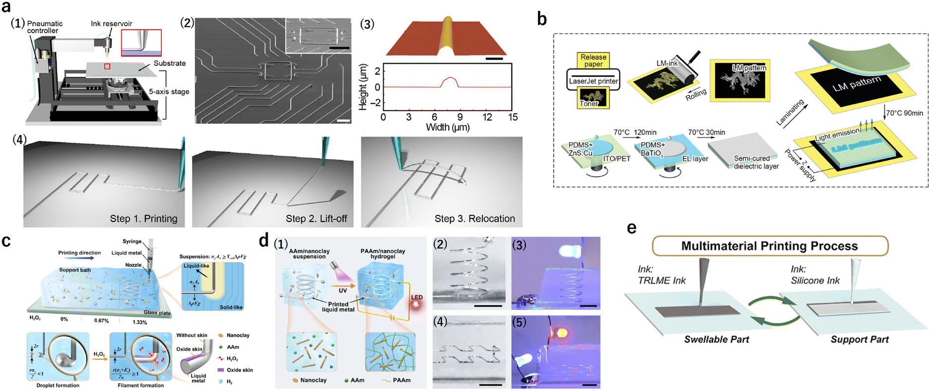 | ||
| Fig. 4 Printing techniques. (a) Direct printing. Reproduced from ref. 39 with permission from American Association for the Advancement of Science (AAAS) copyright 2019. (b) Roller printing. Reproduced from ref. 41 with permission from Wiley & Sons, copyright 2021. (c) and (d) 3D printing in suspension bath. (d-1) Schematic of AAm/nanoclay suspension and (d-2–5) printed 3D structures (helix and double-layered) of liquid metal after and while printing. Reproduced from ref. 42 with permission from Nature, copyright 2022. (e) 4D printing of LM elastomer composites (TRLME). Reproduced from ref. 43 with permission from ACS, copyright 2020. | ||
Wu et al. (2022) demonstrated 3D dangling galinstan structures using a suspension bath. The resolution of the suspension printing strategy for the direct deposition of LM on 3D dangling structures was approximately 150 μm. The suspension bath, which was composed of acrylamide (AAm) and nanoclay, served as a yield-stress fluid support bath with hydrogen peroxide (H2O2) to immediately oxidize the Ga skin and strengthen the extruded LM. The complex 3D structures are manufactured by the free deposition of galinstan filaments in a suspension bath, and they are obtained at a printing velocity of 100 mm min−1 with an extrusion flow rate of 0.040 mL min−1, as shown Fig. 4c. The printing conditions, including the velocity, flow rate, and inner diameter of the nozzle, considerably affected the printing resolution and shape of the fidelity of the LM filaments. When the printing velocity and flow rate were lower and higher, respectively, the structure was continuous but highly heterogeneous with one or more spindle-shaped LM. In contrast, discontinuous or multisegmented filaments with irregular shapes were observed when the velocity was >400 mm min−1 and flow rate was 0.0440 mL min−1. The method could print continuous uniform and polyline/wavy profiles of LM filaments with high shaper fidelity in a support bath within the operating space. Moreover, a polyacrylamide (PAAm)/nanoclay network was formed by introducing the UV light. The printed LM structures became deformable interconnects as the polymerization, and photo crosslinking of AAm contained in the support bath becomes flexible sealing of LM, as shown in Fig. 4d (1). The fabricated helix structure with a pitch of 2 mm and continuous double-layered structure with a vertical distance of 2.5 mm between the two layers are illustrated in Fig. 4d (2, 4), respectively. Furthermore, LM structures were connected to LEDs to verify the electrical conductivity, and LEDs show high conductivity of printed LM in the support bath, as shown in Fig. 4d (3, 5).42 It is appropriate to pattern LM–polymer composites by printing. Zhou et al. (2020) achieved 4D printing of swellable materials based on a thermal-responsive LM elastomer (TRLME), as LM enhanced the thermal conductivity and fracture toughness and decreased the stiffness. This printing completed the bilayer structure, where a swellable TRLME layer and support silicone elastomer layer were sequentially printed.43
Microchannel/microfluidics/direct writing
Galinstan was patterned on a polydimethylsiloxane (PDMS) substrate with designed patterns sealed with water-soluble adhesion tape. For large-sized patterns, acrylic adhesive tape was used because the surface of PDMS is rough and challenging to seal with a thin film. For small patterns, the surface of PDMS can be covered by a polyvinyl alcohol (PVA) thin film since it is smooth. Then, LM is introduced into the channel either by vacuum filling (negative pressure) or by injection with a syringe (positive pressure), as shown in Fig. 5a. Afterward, the sacrificial film was removed via exposure to water. Finally, the LM patterns were packaged by pouring PDMS and curing in an oven to complete the fabrication of the patterning. This technique is advantageous because both negative and positive pressure induced fillings could be used, and a resolution of approximately 30 μm was obtained, which was seven times better than that by masked deposition (resolution of 200 μm). The removal of the sacrificial film does not affect the smoothness of the deposited LM in the channels. Fig. 5a (1–3) shows the LM patterns of serpentine (1), maze (2), and rose (3).44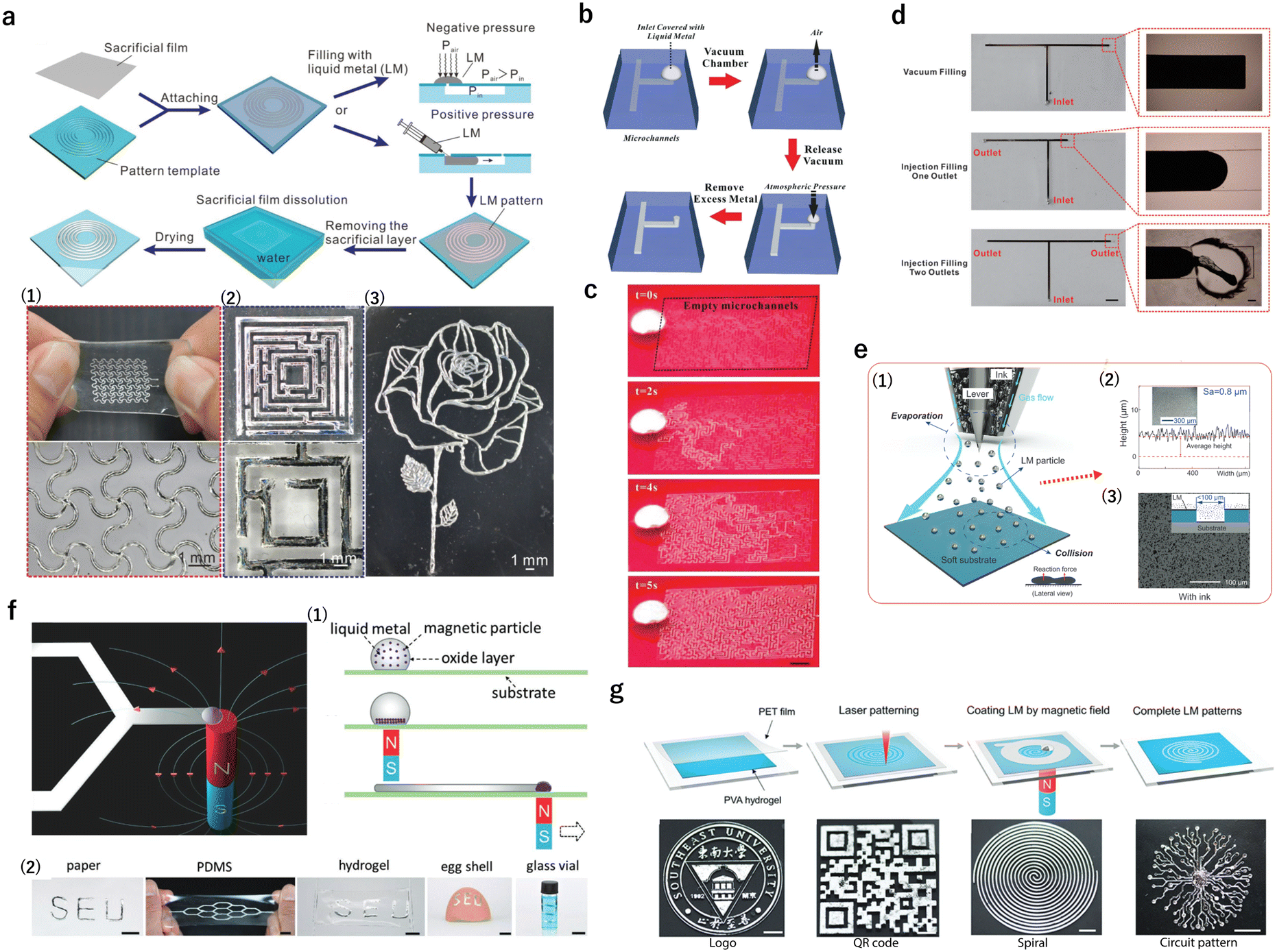 | ||
| Fig. 5 Direct patterning methods. (a) By microfluidic. Reproduced from ref. 44 with permission from RSC, copyright 2019. (b)–(d) Vacuum filling. Reproduced from ref. 45 with permission from RSC, copyright 2017. (e) Thin layer deposition. Reproduced from ref. 46 with permission from Wiley & Sons, copyright 2021. (f) and (g) By magnetic field deposition. Reproduced from ref. 47 and 48 with permission from Wiley & Sons, copyright 2019. | ||
Lin et al. (2017) developed a vacuum filling with only one inlet and no outlets. EGaln was used for vacuum filling. The microfluidic channel had a height of approximately 50 μm, and it was based on PDMS. The inlet was punched to a diameter of 1 mm. The microfluidic device was completed by bonding two PDMS stabs after oxygen plasma treatment. Then, the LM was dropped over the inlet, and the device was placed in a vacuum chamber for approximately 20 min. After releasing the vacuum, the chamber was refilled with atmospheric pressure, forcing the LM to flow into the microchannels. This method was demonstrated using the filling maze as shown in Fig. 5b and c. The maze had a small cross section of 100 μm × 50 μm and many branches with dead ends. The LM filled each part of the microchannel. However, two issues were observed while injecting the air inside the channels and at elevated pressures. Fig. 5d shows the advantages of vacuum filling with only the inlet and no outlets by filling the T-shaped microchannel, compared with one and two outlets. Vacuum filling with only an inlet can completely fill the microchannels, whereas vacuum filling using one outlet can partially fill the T-shaped microchannels.45
Wang et al. (2022) proposed a microscale deposition technique to fabricate a thin and compliant microheater on the abdomen for local ectopic expression in Drosophila. This deposition technique was completed by combining micrometre and sub-micrometre galinstan via collision-triggered rupture of the core shale structure of the particles. Smooth and thin layers with high conductivity and partial gas permeability were produced. The ink consisted of micrometre/sub-micrometre LM particles and solvent, and it was loaded into the airbrush. Afterward, the ink was flown out by high-speed gas. Additionally, LM particles collide with the substrate polymer (mixture of Ecoflex-0030, PDMS, and S3-PDMS) and merge into a continuous conductive LM film, as shown in Fig. 5e (1). The variation in patterned surface height along the line is shown in Fig. 5e (2). The surface roughness was Sa = 0.8 μm, and the film thickness was 5 μm. The graph in Fig. 5e (3) shows that the blobs and splashes of the deposition ink had small homogenous sizes. Thus, the LM particles could pass through microscale openings and reached the bottom target substrate. The micrometre/sub-micrometre particles enable deposition to reach wavy and rough surfaces at micrometre scale, making it suitable for high-resolution patterning.46
In addition, an LM can be patterned using magnetic field. A schematic of the direct patterning of the LM on a planar substrate is shown in Fig. 5f. For this patterning technique, EGaln was mixed with Ni particles. The LM was dropped and adhered to the target substrate. The adhesion of LM was due to the oxide layer on its surface, which not only prevented leakage of the metallic core but also supported adhering metal on various surfaces. After the LM was dropped on the substrate, a permanent magnet was placed under the substrate, and Ni particles were attracted and aggregated at the bottom of the LM droplet. As a sliding magnet to the side, the aggregated Ni particles are pulled and form continuous LM line with a thickness of approximately 10 μm on the substrate, as shown in Fig. 5f (1). Afterward, the excess Ni particles were cleared by a magnet. In this way, LM can be patterned on various substrates, including planar and non-planar surfaces. Fig. 5f (2) illustrates the LM wirings on different substrates, including paper, PDMS, hydrogel, eggshell, and glass vial. This technique is similar to writing by a pen.47 By the same technique as using a magnetic field to pattern LM, Xu et al. (2020) fabricated LM patterning on PVA hydrogel with complex structures. A PVA hydrogel film with a thickness of 500 μm was prepared, and a thin PET film was used to obtain a shadow mask via digital laser printing, on a hydrogel substrate, as shown in Fig. 5g. After mask preparation, EGaln with Ni particles was dropped onto the PET mask. A permanent magnet was placed under the hydrogel, and Ni particles aggregated at the bottom of the LM droplet. Magnetic attraction enhanced the contact between the LM and hydrogel substrate. By moving the magnet, the Ni particles move along the LM through a mask to construct the desired patterns. Afterward, excess LM was removed by tilting the glass substrate followed by absorption of the LM, and a soft squeegee was used to remove excess LM to obtain a smooth LM surface. Finally, the PET mask was removed, and the LM patterns remained on the hydrogel substrate. Fig. 5g illustrates the complex LM patterning on a hydrogel surface with high resolution.48
Although it is advantageous to pattern biphasic LM mixtures by microchannel, microfluidics, or direct printing, there are still challenges including resolutions, precision of small dimension and line edge roughness, and reconfigurability. Patterning LM on curvy surfaces or 3D structures by using these methods is challenging because these methods are often used on flat surfaces. Thus, these methods can be patterned easily with lower surface tension of LM.38,49
Masked depositions
Galinstan was patterned with a shadow mask generated by a laser and transferred to soft substrates of Ecoflex-0030, PDMS, and S3-PDMS. The LM pattern was formed after deposition and mask removal. Owing to the fine size of the LM particles, they can pass through small openings and can reach to the exposed substrate, as shown in Fig. 6a. This enabled high-density deposition with high resolution. As shown in Fig. 6b, the LM is patterned on wavy and rough surfaces and shows good contact with the substrate at the microscale level. It is not only deposited on an uneven surface, but also complex shapes, such as circular, maze, and serpentine are patterned on a smooth surface to demonstrate the capability of patterning complex structures, as illustrated in Fig. 6c.46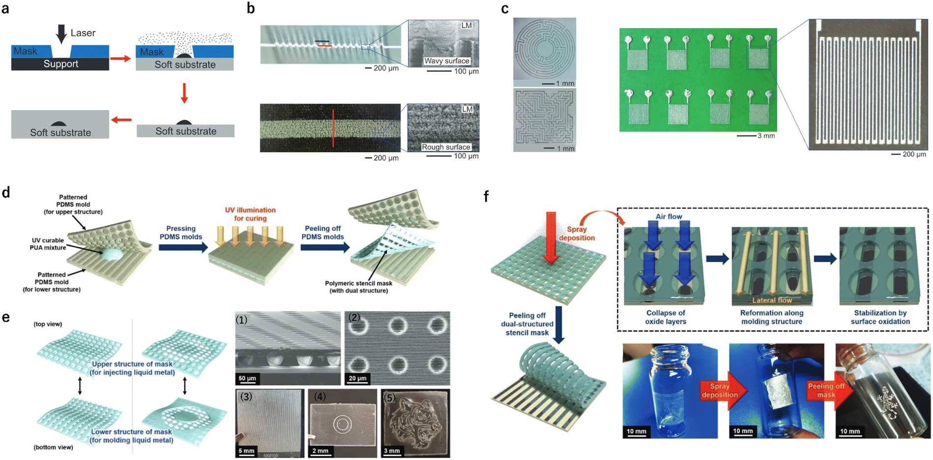 | ||
| Fig. 6 Masked depositions. (a)–(c) Lithography deposition. Reproduced from ref. 46 with permission from Wiley & Sons, copyright 2021. (d)–(f) Fabrication of polymeric stencil mask and patterning LM using this mask. (e-1 and 2) SEM images of the stencil mask and (e-3–5) Photographic images of stencil masks with different shapes and sizes. Reproduced from ref. 50 with permission from Wiley & Sons, copyright 2020. | ||
In addition to shadow mask, a stencil mask can be used to pattern LM. Park et al. (2020) developed a polymeric stencil mask with dual structures based on PDMS, (Fig. 6d). Furthermore, PDMS moulds with two different patterns were prepared corresponding to the upper and lower structures of the stencil mask. Ultra-violet (UV)-curable polyurethane acrylate (PUA) was then drop-cast and sandwiched between two PDMS moulds. The PUA mixture was exposed to the UV light through the moulds for 5 min, and the moulds were peeled off. The polymeric stencil mask was completed without a residual layer in between, and its top and bottom views are illustrated in Fig. 6e. The high-resolution SEM images of the mask and dual structures of various shapes are illustrated in Fig. 6e (1–5). Galinstan was patterned using the polymeric stencil mask via a one-step spray deposition. The quantity of the deposited LM depended on the spraying time, distance, and pressure.50 According to Elassy et al. (2019), spraying time and spraying pressure were varied between 1 and 5 s, and 100 and 500 kPa, respectively. Distance between substrate and nozzle was 5 or 10 cm.51 When spraying, galinstan particles met with the substrate and collapsed their oxide layers. Subsequently, the LM was formed along the lower structure of the mask and was stabilized by surface oxidation. This patterning process is illustrated in Fig. 6f along with patterned design on a glass substrate.50
Applications using biphasic LM mixtures
As LMs have excellent electrical conductivity, in addition to theoretically unlimited extensibility and extremely high flexibility, they have attracted attention as appropriate materials for flexible stretchable or soft applications. They are generally used in flexible or stretchable sensors, and several physical, chemical, and electrical flexible sensors have been reported. LM alloys exhibit better patterning compared to pure LMs, and they show better ability to be utilized in various sensing properties, which pure LMs do not exhibit.LM composite materials with silicone, hydrogel, and other polymers have attracted attention in terms of sensor applications owing to their tunability of electrical characteristics, freestanding properties, and moldability. Here, flexible and stretchable sensors and transistor applications using LM and its alloys and composites are discussed and summarized in Table 1.
| Applications | Materials | Patterning methods | Reference | |
|---|---|---|---|---|
| Sensors | Electronic Tattoo | EGaln/Ni | Printing | 60 |
| ECG patch | EGaln/Ag-SIS polymer | Printing | 62 | |
| Pulse monitor | EGaln/Ni | Direct patterning by magnetic field | 47 | |
| Soft sensor system | EGaln | Direct writing | 65 | |
| Wearable pressure sensor | LM/Fe/PDMS | Lithography/injection | 78 | |
| Pressure-conductive rubber sensor | LM/PDMS | Injection | 77 | |
| Capacitive sensor | EGaln/Ecoflex | Spray coating | 31 | |
| FETs | CNT based transistor | EGaln | Vacuum filling microchannels | 99 |
| Stretchable LM interconnect | EGaln | Hand roller | 112 | |
| SWCNT FET | Galinstan | Spray coating | 113 |
Sensors using LM alloy with solid metal particles
Numerous sensors using LMs have been reported. Furthermore, they have been fabricated by injection into microfluidic channels,52,53 lithography,54 selective wetting with acids and bases,55 formation of microtubes by coaxial injection of LM and polymer,56 and printing processes.57 The sensors were applied to the sensing of bending, pressure, strain, and touch, and they have been used to monitor finger bending,58 pulse rate,57 and pressure distribution on skin.53Although LMs are patterned using various techniques to detect bending, pressure, and strain, their high surface tension generally prevents wiring during fabrication process. However, alloying LM with metal particles can be a solution for reducing surface tension. Mixing Ni particles10 and quartz particles59 in LM can produce LM paste with improved patterning properties while maintaining high elasticity. This can be explained by the fact that the oxide skin (Ga2O3) on the LM surface is dispersed throughout the paste by mixing the particles, which reduces surface tension.60
An E-tattoo based on LM–Ni paste and PMA glue, which is printable on human skin, has been applied to the installation of temperature and touch sensors on the skin,60 as shown in Fig. 7a. In addition, strain sensors fabricated on silicone rubber with LM paste were used for joint bending monitoring.61 In contrast, LM ink based on LM–Ag paste as a matrix and polymer as a binder, are developed and applied for printing ECG measurement devices,62 as shown in Fig. 7b. Thus, the LM–Ag paste was used as a wiring in stretchable touch sensors because of its stability against expansion and contraction.63
 | ||
| Fig. 7 Applications of biphasic LM mixtures-based sensing devices. (a) The touch sensors directory printed on human skin using LM–Ni-paste. Reproduced from ref. 60 with permission from Wiley & Sons, copyright 2019. (b) ECG measurement device printed on silicone elastomer using LM–Ag paste. Reproduced from ref. 62 with permission from Wiley & Sons, copyright 2022. (c) Finger bending measurement device using LM and conventional non-flexible circuit. (d), (e) Connection between LM sensor and gold circuit. (C–E) are reproduced from ref. 65 with permission from ACS, copyright 2019. (f) Conductive-controllable LM–polyurethane composite for soft pressure sensor. Reproduced from ref. 76 with permission from ACS, copyright 2020. (g) Self-healing circuit based on damage-based selective sintering to LM–LCP composite. Reproduced from ref. 80 with permission from National Academy of Sciences (NAS), copyright 2019. (h) Damage detection device based on damage-based selective sintering. Reproduced from ref. 81 with permission from Wiley & Sons, copyright 2019. (i) Capacitive bending sensor using LM–PDMS composite dielectric layer for finger bending monitoring. Reproduced from ref. 31 with permission from ACS, copyright 2019. | ||
Magnetic LM paste can be prepared by mixing magnetic particles, such as Ni and Fe, with LM. Magnetic LM paste was patterned to fabricate strain and pressure sensors using magnetic force, and the sensor was applied to pulse rate monitoring.47 By composing magnetic LM with polymers, the orientation of the LM particles in composites could be achieved by magnetic field. Magnetic LM composites enabled sensors to measure strain by changing the radio-shielding properties.64
Alloying LM with other metals has contributed to the electrical connection between flexible sensors using LM and conventional non-stretch substrates with electronic elements. Kim et al. (2019) investigated the electric contact between LM sensors and different types of materials for a conventional circuit showing that a stable electrical connection is formed between Au, Ag, and LMs,65 as shown in Fig. 7c–e. The result can be explained by the high wettability of LM to Au and Ag and by the alloying of LM–Au and Ag. Sato et al. (2021) investigated the long-term change in electrical connection between Cu electric circuits and LMs and suggested that the difference in contact resistance due to the oxidation layer immediately after device fabrication is eliminated by the alloying of Cu and LMs in the long term.66 The studies provide significant insights into the development of stretchable wearable devices that require a combination of highly stretchable sensors using LMs and non-stretchable conventional integrated circuits.
Due to surface functionalization, LM particles have been used in various chemical sensors. Materials composed of LM particles with zinc, tin, and metal oxides have been used for the measurement of reducing gases67 and heavy metal ions.68 However, chemical sensors based on LM alloys are not applied to wearable devices because high temperature is required for measurement and they can only be used in solution, which may be a crucial issue for future research.
Sensors using a biphasic LM mixture with elastomers
To utilize LM in wearable devices, protection around LM wirings is required to maintain the shape of the wirings, such as encapsulation of the channels with polymer,54 injection into microfluidic channels,53 and sheath-core structure LM fibre formation.69 Therefore, LM–polymer composites (LMPCs), which retain the characteristics of LMs and polymer matrix, are attracting attention as materials for wearable devices. Furthermore, LMPCs are generally fabricated by forming LM droplets by ultrasonic treatment, shear mixing, or other techniques.70 Afterward, they are dispersed in elastomers such as silicone,35 polyurethane, fluoropolymers, or hydrogel.71–73 Additionally, LMPCs are characterized by extremely high deformation, tuneable electrical, and distinctive self-healing properties.74 Furthermore, LMPCs exhibit conductive or dielectric properties, depending on the quantity of LM filler, presence or absence of sintering, and properties of the polymer matrix. Conductive LMPCs are used in resistive mechanical and temperature sensors, whereas dielectric LMPCs are used in capacitive mechanical sensors. In conductive LM-based sensors, when the polymer matrix is insulating, the conductivity of LMPC is caused by the formation of a percolative network of dispersed LM particles.70 Therefore, conductivity can be controlled by adjusting the quantity of LM contained in the matrix.75,76 Peng et al. (2020) demonstrated the high conductivity, low density, high elasticity, and mechanical stability of LM-foam,76 as shown in Fig. 7f. In addition, the conductive property may change due to the rupturing of the oxide layer of LM particles caused by the deformation of the composites by external forces. Owing to its sensitivity to mechanical deformation, conductive LMPC has been used as a pressure76–78 and bending33 sensor. The sensitivity to deformation can be improved by fabricating a structure with a small contact area, owing to the high formability inherent to LMPC. Hu et al. (2021) fabricated hemispherical arrays of PDMS–LM–Fe composites and applied them to human motion state monitoring sensors.78 Furthermore, LMPCs not only respond to external forces but also to temperature changes. Additionally, LMPCs that can reversibly switch between insulation and conduction depending on the temperature change have been developed using the property of LM that solidifies and expands upon cooling.79Sintering by an external force or heat is required for LMPCs to develop electrical conductivity. Selective sintering of only a part of the LMPC can form required conductive paths. Furthermore, owing to the characteristics of external force-induced sintering, conductivity is maintained even in the case of damage to the conductive path as the area around the damage is sintered. Ford et al. (2019) developed a conductive elastomer with self-damage detection utilizing liquid crystal elastomer (LCE)–LM composites and principle of selective sintering owing to damage. The LMPC functions as an integrated sensor–actuator device that expands or contracts in response to damage caused by external forces by combining the thermal deformability of the LCE and self-Joule heating due to the conductivity of LM,80 as shown in Fig. 7g. Markvicka et al. (2019) fabricated a skin-mimicking device that can identify the damaged area using the selective sintering of LMPC due to damage. These self-healing interconnects and damage detection techniques can help to overcome the low durability of flexible devices,81 as shown in Fig. 7h. Additionally, it is crucial for wearable devices that require stable measurements over long periods.
Generally, conductive materials enhance resistance by increasing their length and by decreasing their cross-sectional area due to tensile strain. However, a few LMPCs behave contrary to the Pouillet's law because their conductivity depends on the formation of percolation networks of LMs. The Pouillet's law relates to bulk conductor assumptions and predicts an exponential increase in resistance with stretch due to incompressibility of liquid metal and elastomer. It can be calculated as R = ρL/A where R is resistance, ρ is resistivity, L is length, and A is cross-sectional area. As per Pouillet's law, the resistance changes according to mechanical strain of liquid metal. However, few LMPCs were proposed to exhibit non-Pouillet behaviour. Zolfaghari et al. (2020) fabricated an LMPC whose conductivity did not change with tensile elongation and performed a finite element analysis of the internal percolation conduction paths. They described that the LM droplets in LMPC can be interconnected by forming different shapes of conductive pathways. Thus, they suggested that interconnected liquid metal droplets have tortuosity, unlike pure liquid metal that should follow Pouillet's law. The results confirmed that in the as-fabricated LMPCs, the resistance does not increase with strain.82,83 Yun et al. (2019) developed an LMPC by compositing LM and Fe particles with PDMS, which, contrary to the Pouillet's law, improved the conductivity by tensile elongation,33 and this was applied to monitor finger joint bending. The LMPC was applied to monitor finger joint bending.
Additionally, they developed an LMPC that exhibited anisotropic piezo conductivity to external forces by controlling the orientation of the LM and Fe particles in LMPCs with magnetic forces. This result was applied to a flexible pressure sensor.34 Zheng et al. (2021) developed LM sheath-core fibres that exhibited stable conductivity against elongation utilizing the dipole–dipole interaction between the fluoroelastomer and oxidation layer on the LM nanoparticle surface and applied them to joint bending monitoring using a wearable triboelectric nanogenerator.84 The unique change in electrical properties in response to deformation is a phenomenon that is not observed in pure LM interconnects, such as microfluidic channels, and is expected to expand the range of LMPC applications.
Composited with LM particles are expected to improve thermal and electrical conductivities using an inherently conductive matrix, such as a hydrogel. Liquid metal–hydrogel composites have been applied to self-healing electrical circuits,71–73 wearable sensors for measuring joint bending,71–73,85 pressure and temperature sensors.71,85
For dielectric LMPCs, studies showed that LMPC exhibits a higher dielectric constant than elastomers alone.86,87 Therefore, capacitive mechanical sensors using LMPC as a dielectric have been investigated. Tutika et al. (2019) demonstrated that a composite of LM particles and PDMS exhibited a dielectric constant up to 17 times higher than that of PDMS alone.31 Additionally, they detected subtle differences in finger bending angles using a finger bending sensor fabricated from this composite, as shown in Fig. 7i. Yang et al. (2022) realized a pressure sensor with high sensitivity and a wide detection range by combining a LM composite sponge that deformed under low pressure and pure elastomer layer with relatively low deformability and demonstrated monitoring of joint motion.88 As mentioned, LMPC can be moulded into arbitrary shapes. The performance of pressure sensors can be improved when the dielectric layer has many voids,89 and LMPC, which can be moulded into arbitrary shapes, has attracted attention as a dielectric for pressure sensors. Pressure sensors with dielectric layer structures, such as a flycatcher-like pillar shape90 and sponge shape,86 have been developed using LMPC. The sensors were used to monitor the movement of the human fingers. Although LMPC has been applied to various sensors and devices, its performance as a pure conductor is inferior to that of pure LMs and LM alloys due to sintering requirement for conductivity and percolation dependency for the conductive path. The key advantages of LMPCs, such as easily tuneable electrical properties, self-sustainability, various functionalities derived from the matrix polymers, and percolation conductivity, must be exploited in applications.
Moreover, the LM-based passive electronic tattoo patch is developed for electrophysiological monitoring. The electronic tattoo comprises an ultrathin printed ECG circuit, a battery, and an Ag–In–Ga coil for wireless power transfer system. The printed electrodes provide low-skin electrode (EGaln) impedance and excellent signal to noise ratio. EGaln-based multimodal glove, which is capable of measuring finger movement and provides vibration and thermal feedback, is fabricated including stretchable strain sensors, heater modules, and electrical wires which are made of LM encapsulated by soft elastomers. The multimodal glove is used under VR environments to demonstrate its effectiveness for highly immersive VR. Thus, LM-based soft tactile sensors exhibit low gauge factor in measuring strain and pressure, while the accurate linear response of the LM channel can be used to precisely express the mechanical deformation.91–93
FETs using LMs
Field effect transistors (FETs) have been developed for biomedical applications, such as signal amplification in wearable sensor arrays mounted on the human body and robots.94–96 Liquid metals, and LM-based alloys, and composites are crucial building blocks for realizing stretchable devices because stretchability is required for FETs and are increasingly being introduced into FETs.Flexible FETs have been developed using organic semiconductors and flexible substrates.97,98 However, the devices encountered the challenge of contact failure due to strain. Thus, materials that can withstand strain in the contact area and substrate of stretchable FETs must be considered. Liquid metals are promising contact materials for stretchable FETs. The contact area of an FET consists of three electrodes: source, drain, and gate. Andrews et al. (2018) developed FETs with stretchable and stable LMs as source and drain electrodes.99 EGaIn electrodes are patterned on PDMS substrates with pre-printed CNT channels by direct writing and vacuum filling, as shown in Fig. 8a. The channel width was maintained at 500 μm. The fabricated device exhibited an on–off ratio of 104 and on-current of 75 μA when VDS = −5 V was applied. Ordonez et al. (2017) used LMs as source and drain electrodes to reduce the contact resistance with the graphene channel.16 The galinstan wiring used in this work showed <5.5% change in resistivity after repeated deformation with a curvature radius of 4.5 mm.100 The devices are fabricated in 30 min by dispensing drops of galinstan onto a PET substrate coated with graphene and then dispensing drops of honey, which serve as the gate insulating layer, as shown in Fig. 8b.
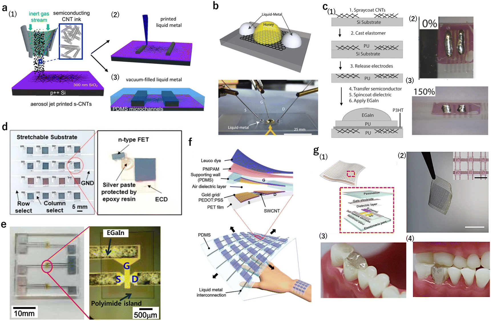 | ||
| Fig. 8 FETs based on LM. (a) Schematics of the fabrication of CNT-FET using printing, direct writing, and vacuum filling. Reproduced from ref. 99 with permission from ACS, copyright 2018. (b) Illustration of a graphene FET with LM source and drain electrodes. Reproduced from ref. 16 with permission from Nature, copyright 2017. (c) FET based on LM gate with fabrication process and strains. Reproduced from ref. 101 with permission from Wiley & Sons, copyright 2014. (d) Optical image of the 4 × 4 stretchable ECD matrix. Reproduced from ref. 111 with permission from Elsevier, copyright 2019. (e) Image of the transistor matrix and LM interconnects transferred to a PDMS substrate. Reproduced from ref. 112 with permission from ACS, copyright 2016. (f) Schematic of temperature sensing FET based on a suspended gate and thermochromic display, and skin attached. Reproduced from ref. 113 with permission from Wiley & Sons, copyright 2018. (g-1 and 2) Schematic and photo of stretchable PD matrix (20 × 20), and (g-3 and 4) images of the stretchable PD array laminated on molar teeth. Reproduced from ref. 114 with permission from Nature, copyright 2022. | ||
In addition, Chortos et al. (2014), who used LM as a gate, developed an FET that exhibited transistor properties even under large strains.101 Furthermore, polyurethane (PU) was used as a substrate, gate insulating layer, CNT as source/drain electrodes, and poly(3-hexylthiophene-2,5-diyl) (P3HT) as an organic semiconductor. The LM used in this device is patterned using a syringe and needle, as shown in Fig. 8c. The device was characterized by its ability to accommodate strain in two directions. On–current was produced 0.4 and 0.5 times when applying 70% of strain vertically, and 100% of strain horizontally, respectively, compared to the case where no strain was applied. When LMs were used in the contact area, an issue of current modulation was observed due to the strain caused by electrode deformation. The deformation of the electrode should be considered, along with the degradation of the channel material due to expansion and contraction.102 Especially, when FETs are used as signal amplifiers, modulation of the on–current is a major challenge.
Transistor matrix based on LM interconnection
Research into biomedical applications using FETs has been conducted to develop transistor matrices that are compatible with applying to the human body.103–106 Thus, such applications should be stretchable or flexible. Therefore, the transistor matrix should be fabricated on stretchable substrate along with stretchable materials by replacing rigid materials. The highly conducting metals such as Au and Ag are often used as wiring materials. Combining them into elastomeric materials including poly (vinylidene fluoride-co-hexafluoropropylene) and styrene–butadiene–styrene improves stretchability. Recently, they have been replaced with LMs which are highly conductive and deformable. LM provides both metallic and fluidic properties that ensure novel applications.107–109 Percolation networks of metal nanowires are suitable for serving as stretchable conducting materials. The EGaln has high conductivity, low toxicity, high deformability, and excellent biocompatibility and has been actively used in the stretchable electrode, such as the gate electrode. EGaln is usually combined with elastomers to improve the stretchability and stability. Moreover, LM can be deposited by either microchannel filling or contact printing. The vacuum microchannel filling deposition is used for realizing high performance FETs with low contact resistance.99,110 Inorganic FETs can be combined with LMs to construct the transistor matrices. Kim et al. (2019) developed a stretchable display by combining electrochromic devices and FETs, and they use LM wiring,111 as shown in Fig. 8d. 4 × 4-pixel transistor matrices were constructed on a stretchable Ecoflex, and the LM interconnections were patterned by spray coating. Transistor matrices showed mechanical stability to 30% biaxial strain and bending radius of 20 mm.Organic field-effect transistors (OFETs) were combined with LMs to construct transistor matrices. Park et al. (2016) developed transistor matrices interconnected by EGaln that was patterned by photolithography on a polyimide substrate for OFETs112 (Fig. 8e). The polyimide substrate made it challenging FET parts to deform, even when the entire structure was stretched significantly. For strains up to 50%, Hong et al. (2019) developed a temperature sensor matrix consisting of OFETs and LM interconnects.113 The highly sensitive and stretchable temperature sensor array was based on an active matrix comprising single walled carbon nanotube (SWCNT) FETs. The FET is composed of poly(N-isopropylacrylamide) (PNIPAM) coated gold grid/PEDOT:PSS as gate electrode, and thermochromic leuco dye that changes its colour depending on the temperature, SWCNT channel and air-dielectric layer, as shown in Fig. 8f. The FET arrays were formed by patterning source, gate, and drain gold grid/PEDOT:PSS film on PET film. The contacts were a combination of PEDOT:PSS and Au wire, making the OFET stretchable. Subsequently, a 4 × 6 transistor matrix was constructed. The fabricated temperature sensor matrix showed a stable output for 50% of strain in two axial directions, and when worn on the wrist, spatial mapping of temperature was possible regardless of movement. This is because the strain was concentrated on the substrate rather than on the element. Thus, the use of LMs for FET interconnections has led to the development of transistor matrices for stretchable substrates. The use of Si-based FETs on stretchable substrates and making the substrate of the FET stiffer than the element part suppresses deformation of the element part. A FET-based sensor requires an element part that does not deform, as well as a practical LM interconnection.
FETs based on biphasic LM mixtures
For FET-based wearable applications, electrodes, and wiring from LMs with solid conductor electrodes must be replaced.100 Furthermore, FETs cannot be made practical using LMs, which are unstable in shape. Simply replacing the LM with a solid metal such as Au or Al is not sufficient to fabricate an elastic FET. Therefore, LM alloys and LM composites have attracted considerable attention as new electrode materials.Kim et al. (2022) developed a sensor matrix for tooth crack detection using stretchable self-healing interconnects made of LM and Ag composite (Ag–EGaln alloy)114 (Fig. 8g). The Ag–EGaln alloy was used for wiring to construct a 20 × 20 transistor matrix. Phosphor particles and a photodetector (PD) were introduced into the matrix for in vivo detection of tooth microcracks. The Ag–LM alloy exhibited an electrical conductivity of approximately 2 S μm−1. Stretching and self-healing of the Ag–LM alloy consisted of three processes. When the wiring was broken by expansion and contraction, the oxide film on the LM surface was broken causing the LM to flow out of the cross-section. The influx of LM connected adjacent Ag cross-sections and restored the electrical conductivity. Self-healing occurred within a few milliseconds. LM alloys and composites are useful for fabricating devices that are more practical because the interconnection of LMs in sensor applications is practical. Stretchable interconnections based on LM alloys and composites, which cannot be realized with solid electrodes, are expected to be used to build transistor matrices for biomedical applications in the future.
Conclusions
This review presents biphasic LM mixture-based applications along with the methodologies of fabrication and patterning. Biphasic LM mixtures are generally made with other metals, such as Ni, Cu, and Fe, and composites with elastomers, such as PDMS and Ecoflex. Printing is most appropriate for patterning both LM with solid metal particles and elastomers. Furthermore, stretchable, and flexible applications, such as sensors and FETs using LM and its mixtures with other metals and elastomers, are discussed. Liquid metals or LM alloys with solid metal particles used in stretchable sensors ensure high processability and elasticity, whereas LM–polymer composites attracting attention owing to their tuneable electrical properties, and free-standing nature. In contrast, LMs are generally used as contacts and wirings of stretchable FETs for practical applications, such as FET-based sensor. Biphasic LM mixtures with polymers have potential for use in biomedical applications of FETs.The biphasic structured LM mixtures have shown significant potential for improvements in stretchable and flexible applications, especially in different kinds of sensors. Furthermore, the restrained conductivity of LMs because of the oxide layer or soft elastomers formed outside the LM should be addressed.
Thus, toxicity of LM should be considered for further improvements of its applications because the LM tends to show more toxicity in the nanoscale than that in the bulk scale. Furthermore, toxicity and biocompatibility of LMs in environment where metal ions are easier to produce should be considered.115 The soft and wearable electronics based on liquid metal and liquid metal composites are dependent on the manufacturing techniques for mass production.116 In the case of LM composites, their synthesis has been performed in a laboratory on a small scale; however, the techniques which ensure equal mixing ratios throughout synthesizing should be implemented in large-scale production. Moreover, LMPCs are often unstable due to uneven mixing and percolation dependent conductive pathways. Thus, the stability of liquid metal should be considered to ensure fine patterning of liquid metal by printing instruments.
Further implementation of liquid metals as electrical materials is expected to gradually increase because efficient wiring methods are still under development. However, liquid metals for heat transfer materials will be rapidly developed as they are already practically used as thermal conductive materials in some electronic devices. The development of biphasic liquid metal composites as wiring materials and heat transfer materials would gain attention in the future. Research on the functionalization of liquid metals may become important for the future expansion of applications based on liquid metal. It is believed that liquid metal-based devices will be commercialized in the near future, especially in healthcare applications. Furthermore, biphasic liquid metal can enable new applications along with opportunities for use in interdisciplinary fields. Owing to its unique property of exhibiting both metallic and fluidic properties, new paths for use in various fields including building materials and space technology can be opened.
Conflicts of interest
The authors declare no conflicts of interest.Acknowledgements
This work was supported by JSPS KAKENHI (Grant: 20H00213), JST CREST (Grant: JP19209665), and JST AIP Acceleration Research (Number: JPMJCR22U2), Japan.References
- M. Li, Y. Wu, L. Zhang, H. Wo, S. Huang, W. Li, X. Zeng, Q. Ye, T. Xu, J. Luo, S. Dong, Y. Li, H. Jina and X. Wang, Nanoscale, 2019, 11, 5441–5449 RSC.
- Q. Shi, B. Dong, T. He, Z. Sun, J. Zhu, Z. Zhang and C. Lee, InfoMat, 2020, 2, 1131–1162 CrossRef.
- S. Nie, M. Cai, H. Yang, L. Shen, S. Wang, Y. Zhu and J. Song, npj Flexible Electron., 2022, 6, 36 CrossRef CAS.
- H. Ullah, M. A. Wahab, G. Will, M. R. Karim, T. Pan, M. Gao, D. Lai, Y. Lin and M. H. Miraz, Biosensors, 2022, 12, 630 CrossRef CAS PubMed.
- F. Catania, H. de Souza Oliveira, P. Lugoda, G. Cantarella and N. Münzenrieder, J. Phys. D: Appl. Phys., 2022, 55, 323002 CrossRef.
- C. Wang, K. Xia, H. Wang, X. Liang, Z. Yin and Y. Zhang, Adv. Mater., 2019, 31, 1801072 CrossRef PubMed.
- Y. Pang, Z. Yang, Y. Yang and T.-L. Ren, Small, 2020, 16, 1901124 CrossRef CAS PubMed.
- J. Lee, B. L. Zambrano, J. Woo, K. Yoon and T. Lee, Adv. Mater., 2020, 32, 1902532 CrossRef CAS PubMed.
- Y. Lin, J. Genzer and M. D. Dickey, Adv. Sci., 2020, 7, 2000192 CrossRef CAS PubMed.
- U. Daalkhaijav, O. D. Yirmibesoglu, S. Walker and Y. Mengüç, Adv. Mater. Technol., 2018, 3, 1700351 CrossRef.
- X. Sun, X. Wang, B. Yuan and J. Liu, Mater. Today Phys., 2020, 14, 100245 CrossRef.
- M. D. Dickey, Adv. Mater., 2017, 29, 1606425 CrossRef PubMed.
- M. Baharfar and K. Kalantar-Zadeh, ACS Sens., 2022, 7, 386–408 CrossRef CAS PubMed.
- Y. Ren, X. Sun and J. Liu, Micromachines, 2020, 11, 200 CrossRef PubMed.
- Y.-L. Chen, Y. Nguyen, S.-E. Wu, Y.-C. Chin, C. Chuang, Y.-P. Hsieh and M. Hofmann, Nanoscale, 2020, 12, 4751 RSC.
- R. C. Ordonez, C. K. Hayashi, C. M. Torres, J. L. Melcher, N. Kamin, G. Severa and D. Garmire, Sci. Rep., 2017, 7, 10171 CrossRef PubMed.
- A. Hajalilou, A. F. Silva, P. A. Lopes, E. Parvini, C. Majidi and M. Tavakoli, Adv. Mater. Interfaces, 2022, 9, 2101913 CrossRef CAS.
- X. Wang, W. Yao, R. Guo, X. Yang, J. Tang, J. Zhang, W. Gao, V. Timchenko and J. Liu, Adv. Healthcare Mater., 2018, 7, 1800318 CrossRef PubMed.
- X. Sun, B. Yuan, L. Sheng, W. Rao and J. Liu, Appl. Mater. Today, 2020, 20, 100722 CrossRef.
- X. Deng, G. Chen, Y. Liao, X. Lu, S. Hu, T. Gan, S. Handschuh-Wang and X. Zhang, Polymers, 2022, 14, 2259 CrossRef CAS PubMed.
- H. Bark and P. S. Lee, Chem. Sci., 2021, 12, 2760–2777 RSC.
- S. Chen, H. Z. Wang, R. Q. Zhao, W. Rao and J. Liu, Matter, 2020, 2, 1446–1480 CrossRef.
- M.-Z. Li, S.-T. Han and Y. Zhou, Adv. Intell. Syst., 2020, 2, 2000113 CrossRef.
- Y. H. Lee, M. Jang, M. Y. Lee, O. Y. Kweon and J. H. Oh, Chem, 2017, 3, 724–763 CAS.
- Q. Wang, Y. Yu and J. Liu, Adv. Eng. Mater., 2018, 20, 1700781 CrossRef.
- H. Wang, B. Yuan, S. Liang, R. Guo, W. Rao, X. Wang, H. Chang, Y. Ding, J. Liu and L. Wang, Mater. Horiz., 2018, 5, 222–229 RSC.
- S. Ki, J. Shim, S. Oh, E. Koh, D. Seo, S. Ryu, J. Kim and Y. Nam, Int. J. Heat Mass Transfer, 2021, 170, 121012 CrossRef CAS.
- J. Tang, X. Zhao, J. Li, R. Guo, Y. Zhou and J. Liu, ACS Appl. Mater. Interfaces, 2017, 9, 35977–35987 CrossRef CAS PubMed.
- H. Chang, R. Guo, Z. Sun, H. Wang, Y. Hou, Q. Wang, W. Rao and J. Liu, Adv. Mater. Interfaces, 2018, 5, 1800571 CrossRef.
- S. Y. Tang and R. Qiao, Acc. Mater. Re, 2021, 2, 966–978 CrossRef CAS.
- R. Tutika, S. Kmiec, A. B. M. Tahidul Haque, S. W. Martin and M. D. Bartlett, ACS Appl. Mater. Interfaces, 2019, 11, 17873–17883 CrossRef CAS PubMed.
- C. J. Thrasher, Z. J. Farrell, N. J. Morris, C. L. Willey and C. E. Tabor, Adv. Mater., 2019, 31, 1903864 CrossRef CAS PubMed.
- G. Yun, S. Y. Tang, S. Sun, D. Yuan, Q. Zhao, L. Deng, S. Yan, H. Du, M. D. Dickey and W. Li, Nat. Commun., 2019, 10, 1300 CrossRef PubMed.
- G. Yun, S. Y. Tang, Q. Zhao, Y. Zhang, H. Lu, D. Yuan, S. Sun, L. Deng, M. D. Dickey and W. Li, Matter, 2020, 3, 824–841 CrossRef.
- M. G. Saborio, S. Cai, J. Tang, M. B. Ghasemian, M. Mayyas, J. Han, M. J. Christoe, S. Peng, P. Koshy, D. Esrafilzadeh, R. Jalili, C. H. Wang and K. Kalantar-Zadeh, Small, 2020, 16, 1903753 CrossRef CAS PubMed.
- Y. Sohn and K. Chu, Mater. Lett., 2020, 265, 127223 CrossRef CAS.
- C. Cho, W. Shin, M. Kim, J. Bang, P. Won, S. Hong and S. H. Ko, Small, 2022, 18, 2202841 CrossRef CAS PubMed.
- I. D. Joshipura, H. R. Ayers, C. Majidi and M. D. Dickey, J. Mater. Chem. C, 2015, 3, 3834–3841 RSC.
- Y. G. Park, H. S. An, J. Y. Kim and J. U. Park, Sci. Adv., 2019, 5, eaaw2844 CrossRef CAS PubMed.
- G. Shin, B. Jeon and Y. L. Park, J. Micromech. Microeng., 2020, 30, 034001 CrossRef CAS.
- Z. Zhou, Y. Yao, C. Zhang, Z. Deng, Q. Li, Q. Wang and J. Liu, Adv. Mater. Technol., 2022, 7, 2101010 CrossRef CAS.
- Q. Wu, F. Zhu, Z. Wu, Y. Xie, J. Qian, J. Yin and H. Yang, npj Flexible Electron., 2022, 6, 50 CrossRef CAS.
- L.-Y. Zhou, J.-H. Ye, J.-Z. Fu, Q. Gao and Y. He, ACS Appl. Mater. Interfaces, 2020, 12, 12068–12074 CrossRef CAS PubMed.
- L. Teng, L. Zhu, S. Handschuh-Wang and X. Zhou, J. Mater. Chem. C, 2019, 7, 15243–15251 RSC.
- Y. Lin, O. Gordon, M. R. Khan, N. Vasquez, J. Genzer and M. D. Dickey, Lab Chip, 2017, 17, 3043–3050 RSC.
- B. Wang, J. Gao, J. Jiang, Z. Hu, K. Hjort, Z. Guo and Z. Wu, Adv. Mater. Technol., 2022, 7, 2100903 CrossRef CAS.
- B. Ma, C. Xu, J. Chi, J. Chen, C. Zhao and H. Liu, Adv. Funct. Mater., 2019, 29, 1901370 CrossRef.
- C. Xu, B. Ma, S. Yuan, C. Zhao and H. Liu, Adv. Electron. Mater., 2020, 6, 1900721 CrossRef CAS.
- J. Ma, F. Krisnadi, M. H. Vong, M. Kong, O. M. Awartani and M. D. Dickey, Adv. Mater., 2022, 2205196 CrossRef PubMed.
- T. H. Park, J. H. Kim and S. Seo, Adv. Funct. Mater., 2020, 30, 2003694 CrossRef CAS.
- K. S. Elassy, T. K. Akau, W. A. Shiroma, S. Seo and A. T. Ohta, Appl. Sci., 2019, 9, 1565 CrossRef CAS.
- Y. Wang, Y. Lu, D. Mei and L. Zhu, IEEE Sens. J., 2021, 21, 1694–1703 CAS.
- Y. Gao, H. Ota, E. W. Schaler, K. Chen, A. Zhao, W. Gao, H. M. Fahad, Y. Leng, A. Zheng, F. Xiong, C. Zhang, L.-C. Tai, P. Zhao, R. S. Fearing and A. Javey, Adv. Mater., 2017, 29, 1701985 CrossRef PubMed.
- Y. R. Jeong, J. Kim, Z. Xie, Y. Xue, S. M. Won, G. Lee, S. W. Jin, S. Y. Hong, X. Feng, Y. Huang, J. A. Rogers and J. S. Ha, NPG Asia Mater., 2017, 9, e443 CrossRef CAS.
- Y. Wu, Y. Zhou, W. Asghar, Y. Liu, F. Li, D. Sun, C. Hu, Z. Wu, J. Shang, Z. Yu, R.-W. Li and H. Yang, Adv. Intell. Syst., 2021, 3, 2000235 CrossRef.
- X. Yu, W. Fan, Y. Liu, K. Dong, S. Wang, W. Chen, Y. Zhang, L. Lu, H. Liu and Y. Zhang, Adv. Mater. Technol., 2022, 7, 2101618 CrossRef CAS.
- G. Li, F. Sun, H. Chen, Y. Jin, A. Zhang and J. Du, ACS Appl. Mater. Interfaces, 2021, 13, 56961–56971 CrossRef CAS PubMed.
- J. Chen, J. Zhang, Z. Luo, J. Zhang, L. Li, Y. Su, X. Gao, Y. Li, W. Tang, C. Cao, Q. Liu, L. Wang and H. Li, ACS Appl. Mater. Interfaces, 2020, 12, 22200–22211 CrossRef CAS PubMed.
- H. Chang, P. Zhang, R. Guo, Y. Cui, Y. Hou, Z. Sun and W. Rao, ACS Appl. Mater. Interfaces, 2020, 12, 14125–14135 CrossRef CAS PubMed.
- R. Guo, X. Sun, S. Yao, M. Duan, H. Wang, J. Liu and Z. Deng, Adv. Mater. Technol., 2019, 4, 1900183 CrossRef CAS.
- C. Votzke, U. Daalkhaijav, Y. Mengüç and M. L. Johnston, IEEE Biomed. Circuits Syst. Conf., 2018, 1–4 Search PubMed.
- W. Zu, Y. Ohm, M. R. Carneiro, M. Vinciguerra, M. Tavakoli and C. Majidi, Adv. Mater. Technol., 2022, 2200534 CrossRef CAS.
- J. Wang, G. Cai, S. Li, D. Gao, J. Xiong and P. S. Lee, Adv. Mater., 2018, 30, 1706157 CrossRef PubMed.
- R. Zhu, Z. Li, G. Deng, Y. Yu, J. Shui, R. Yu, C. Pan and X. Liu, Nano Energy, 2022, 92, 106700 CrossRef CAS.
- S. Kim, J. Oh, D. Jeong and J. Bae, ACS Appl. Mater. Interfaces, 2019, 11, 20557–20565 CrossRef CAS PubMed.
- T. Sato, K. Yamagishi, M. Hashimoto and E. Iwase, ACS Appl. Mater. Interfaces, 2021, 13, 18247–18254 CrossRef CAS PubMed.
- S. A. Idrus-Saidi, J. Tang, J. Yang, J. Han, T. Daeneke, A. P. O'Mullane and K. Kalantar-Zadeh, ACS Sens., 2020, 5, 1177–1189 CrossRef CAS PubMed.
- W. Zhang, J. Z. Ou, S.-Y. Tang, V. Sivan, D. D. Yao, K. Latham, K. Khoshmanesh, A. Mitchell, A. P. O'Mullane and K. Kalantar-zadeh, Adv. Funct. Mater., 2014, 24, 3799–3807 CrossRef CAS.
- C. B. Cooper, K. Arutselvan, Y. Liu, D. Armstrong, Y. Lin, M. R. Khan, J. Genzer and M. D. Dickey, Adv. Funct. Mater., 2017, 27, 1605630 CrossRef.
- N. Kazem, T. Hellebrekers and C. Majidi, Adv. Mater., 2017, 29, 1605985 CrossRef PubMed.
- C. Wang, J. Li, Z. Fang, Z. Hu, X. Wei, Y. Cao, J. Han and Y. Li, Macromol. Rapid Commun., 2022, 43, 2100543 CrossRef CAS PubMed.
- M. Liao, H. Liao, J. Ye, P. Wan and L. Zhang, ACS Appl. Mater. Interfaces, 2019, 11, 47358–47364 CrossRef CAS PubMed.
- Z. Zhou, C. Qian and W. Yuan, Compos. Sci. Technol., 2021, 203, 108608 CrossRef CAS.
- G. G. Guymon and M. H. Malakooti, J. Polym. Sci., 2022, 60, 1300–1327 CrossRef CAS.
- J. Xu, H. Pang, X. Gong, L. Pei and S. Xuan, iScience, 2021, 24, 102549 CrossRef PubMed.
- Y. Peng, H. Liu, T. Li and J. Zhang, ACS Appl. Mater. Interfaces, 2020, 12, 6489–6495 CrossRef CAS PubMed.
- J. H. Oh, J. Y. Woo, S. Jo and C.-S. Han, Sens. Actuators, A, 2019, 299, 111610 CrossRef CAS.
- W. Hu, Y. Li, S.-Y. Tang, L. Li, Q. J. Niu and S. Yan, Adv. Mater. Interfaces, 2021, 8, 2100038 CrossRef CAS.
- H. Wang, Y. Yao, Z. He, W. Rao, L. Hu, S. Chen, J. Lin, J. Gao, P. Zhang, X. Sun, X. Wang, Y. Cui, Q. Wang, S. Dong, G. Chen and J. Liu, Adv. Mater., 2019, 31, 1901337 CrossRef PubMed.
- M. J. Ford, C. P. Ambulo, T. A. Kent, E. J. Markvicka, C. Pan, J. Malen, T. H. Ware and C. Majidi, Proc. Natl. Acad. Sci. U. S. A., 2019, 116, 21438–21444 CrossRef CAS PubMed.
- E. J. Markvicka, R. Tutika, M. D. Bartlett and C. Majidi, Adv. Funct. Mater., 2019, 29, 1900160 CrossRef.
- L. Sanchez-Botero, D. S. Shah and R. Kramer-Bottiglio, Adv. Mater., 2022, 2109427 CrossRef CAS PubMed.
- N. Zolfaghari, P. Khandagale, M. J. Ford, K. Dayal and C. Majidi, Soft Matter, 2020, 16, 8818–8825 RSC.
- L. Zheng, M. Zhu, B. Wu, Z. Li, S. Sun and P. Wu, Sci. Adv., 2021, 7, 4041–4069 CrossRef PubMed.
- Z. Zhang, L. Tang, C. Chen, H. Yu, H. Bai, L. Wang, M. Qin, Y. Feng and W. Feng, J. Mater. Chem. A, 2021, 9, 875–883 RSC.
- J. Yang, D. Tang, J. Ao, T. Ghosh, T. V. Neumann, D. Zhang, Y. Piskarev, T. Yu, V. K. Truong, K. Xie, Y.-C. Lai, Y. Li and M. D. Dickey, Adv. Funct. Mater., 2020, 30, 2002611 CrossRef CAS.
- M. D. Bartlett, A. Fassler, N. Kazem, E. J. Markvicka, P. Mandal and C. Majidi, Adv. Mater., 2016, 28, 3726–3731 CrossRef CAS PubMed.
- J. Yang, K. Y. Kwon, S. Kanetkar, R. Xing, P. Nithyanandam, Y. Li, W. Jung, W. Gong, M. Tuman, Q. Shen, M. Wang, T. Ghosh, K. Chatterjee, X. Wang, D. Zhang, T.-I. Kim, V. K. Truong and M. D. Dickey, Adv. Mater. Technol., 2022, 7, 2101074 CrossRef CAS.
- J. Qin, L.-J. Yin, Y.-N. Hao, S.-L. Zhong, D.-L. Zhang, K. Bi, Y.-X. Zhang, Y. Zhao and Z.-M. Dang, Adv. Mater., 2021, 33, 2008267 CrossRef CAS PubMed.
- D. Zhang, Y. Zhong, Y. Wu, X. Zhang, M. D. Dickey and J. Yang, Compos. Sci. Technol., 2021, 216, 109066 CrossRef CAS.
- J. Alberto, C. Leal, C. Fernandes, P. A. Lopes, H. Paisana, A. T. de Almeida and M. Tavakoli, Sci. Rep., 2020, 10, 5539 CrossRef PubMed.
- J. Oh, S. Kim, S. Lee, S. Jeong, S. H. Ko and J. Bae, Adv. Funct. Mater., 2021, 31, 2007772 CrossRef CAS.
- P. Won, S. Jeong, C. Majidi and S. H. Ko, iScience, 2021, 24, 102698 CrossRef CAS PubMed.
- R. A. Nawrocki, N. Matsuhisa, T. Yokota and T. Someya, Adv Electron. Mater., 2016, 2, 1500452 CrossRef.
- X. Ren, K. Pei, B. Peng, Z. Zhang, Z. Wang, X. Wang and P. K. L. Chan, Adv. Mater., 2016, 28, 4832–4838 CrossRef CAS PubMed.
- S. Wang, J. Xu, W. Wang, G.-J. N. Wang, R. Rastak, F. Molina-Lopez, J. W. Chung, S. Niu, V. R. Feig, J. Lopez, T. Lei, S.-K. Kwon, Y. Kim, A. M. Foudeh, A. Ehrlich, A. Gasperini, Y. Yun, B. Murmann, J. B.-H. Tok and Z. Bao, Nature, 2018, 555, 83–88 CrossRef CAS PubMed.
- T. Someya, T. Sekitani, S. Iba, Y. Kato, H. Kawaguchi and T. Sakurai, Proc. Natl. Acad. Sci. U. S. A., 2004, 101, 9966–9970 CrossRef CAS PubMed.
- J. Huang, H. Zhu, Y. Chen, C. Preston, K. Rohrbach, J. Cumings and L. Hu, ACS Nano, 2013, 7, 2106–2113 CrossRef CAS PubMed.
- J. B. Andrews, K. Mondal, T. V. Neumann, J. A. Cardenas, J. Wang, D. P. Parekh, Y. Lin, P. Ballentine, M. D. Dickey and A. D. Franklin, ACS Nano, 2018, 12, 5482–5488 CrossRef CAS PubMed.
- R. C. Ordonez, C. K. Hayashi, C. M. Torres, N. Hafner, J. R. Adleman, N. M. Acosta, J. Melcher, N. M. Kamin and D. Garmire, IEEE Trans. Electron Devices, 2016, 63, 4018–4023 CAS.
- A. Chortos, J. Lim, J. W. F. To, M. Vosgueritchian, T. J. Dusseault, T.-H. Kim, S. Hwang and Z. Bao, Adv. Mater., 2014, 26, 4253–4259 CrossRef CAS PubMed.
- D.-Y. Khang, J. A. Rogers and H. H. Lee, Adv. Funct. Mater., 2009, 19, 1526–1536 CrossRef CAS.
- Y.-L. Loo, T. Someya, K. W. Baldwin, Z. Bao, P. Ho, A. Dodabalapur, H. E. Katz and J. A. Rogers, Proc. Natl. Acad. Sci. U. S. A., 2002, 99, 10252–10256 CrossRef CAS PubMed.
- T. Sekitani and T. Someya, Adv. Mater., 2010, 22, 2228–2246 CrossRef CAS PubMed.
- G. Kettlgruber, M. Kaltenbrunner, C. M. Siket, R. Moser, I. M. Graz, R. Schwödiauera and S. Bauer, J. Mater. Chem. A, 2013, 1, 5505–5508 RSC.
- M. Kaltenbrunner, T. Sekitani, J. Reeder, T. Yokota, K. Kuribara, T. Tokuhara, M. Drack, R. Schwödiauer, I. Graz, S. Bauer-Gogonea, S. Bauer and T. Someya, Nature, 2013, 499, 458–463 CrossRef CAS PubMed.
- B. Wang and A. Facchetti, Adv. Mater., 2019, 31, 1901408 CrossRef PubMed.
- S. Choi, S. I. Han, D. Jung, H. J. Hwang, C. Lim, S. Bae, O. K. Park, C. M. Tschabrunn, M. Lee, S. Y. Bae, J. W. Yu, J. H. Ryu, S.-W. Lee, K. Park, P. M. Kang, W. B. Lee, R. Nezafat, T. Hyeon and D.-H. Kim, Nat. Nanotechnol., 2018, 13, 1048–1056 CrossRef CAS PubMed.
- S. Huang, Y. Liu, Y. Zhao, Z. Ren and C. F. Guo, Adv. Funct. Mater., 2019, 29, 1805924 CrossRef.
- F. Wu, Y. Liu, J. Zhang, S. Duan, D. Ji and H. Yang, Small Methods, 2021, 5, 2100676 CrossRef CAS PubMed.
- D. S. Kim, H. Park, S. Y. Hong, J. Yun, G. Lee, J. H. Lee, L. Sun, G. Zi and J. S. Ha, Appl. Surf. Sci., 2019, 471, 300–308 CrossRef CAS.
- C. W. Park, Y. G. Moon, H. Seong, S. W. Jung, J.-Y. Oh, B. S. Na, N.-M. Park, S. S. Lee, S. G. Im and J. B. Koo, ACS Appl. Mater. Interfaces, 2016, 8, 15459–15465 CrossRef CAS PubMed.
- S. Y. Hong, M. S. Kim, H. Park, S. W. Jin, Y. R. Jeong, J. W. Kim, Y. H. Lee, L. Sun, G. Zi and J. S. Ha, Adv. Funct. Mater., 2019, 29, 1807679 CrossRef.
- H. J. Kim, S. Ji, J. Y. Han, H. B. Cho, Y.-G. Park, D. Choi, H. Cho, J.-U. Park and W. B. Im, NPG Asia Mater., 2022, 14, 26 CrossRef CAS.
- S. Chen, R. Zhao, X. Sun, H. Wang, L. Li and J. Liu, Adv. Healthcare Mater., 2022, 2201924 Search PubMed.
- K. B. Ozutemiz, C. Majidi and O. B. Ozdoganlar, Adv. Mater. Technol., 2022, 7, 2200295 CrossRef CAS.
| This journal is © The Royal Society of Chemistry 2023 |