
 Open Access Article
 This Open Access Article is licensed under a Creative Commons Attribution-Non Commercial 3.0 Unported Licence
A highly stable room temperature titania nanostructure-based thin film transistor (TFT) alcohol sensor
Aditya Kumar
Singh
and
Basanta
Bhowmik
 *
*
Thin Film Device Laboratory, Department of Electronics and Communication Engineering, National Institute of Technology, Jamshedpur-831014, India. E-mail: bb.cemk.ece@gmail.com
First published on 5th December 2022
Abstract
The present study is concerned with the room temperature field-induced alcohol sensitivity of nanostructured TiO2 thin films in field-effect transistor (TFT) configurations. The structural, morphological and optical characterizations of the TiO2 thin film (grown via a low-cost solution process) revealed that the thickness of the film was ∼220 nm with numerous pores on the surface. The average particle size was found to be 22 nm from XRD characterization. The surface roughness of the film was 215 nm. Photoluminescence studies showed that the TiO2 band was 3.12 eV. The presence of oxygen vacancies and defect states was confirmed through PL spectroscopy and XPS studies. Electrical characteristics revealed a device mobility of ∼13 cm2 V−1 s−1, ION/IOFF ratio of ∼2.16 × 10⁴, subthreshold swing of ∼31.4 mV dec−1 and threshold voltage of 0.65 V. The tuning of carrier concentrations at the sensing channel was achieved through gate biasing in the presence of vapor concentrations. At room temperature, exposure to ethanol, methanol and 2-propanol revealed a drastic drain current variation with shifts in the threshold voltage (Vth) for fixed Vgs and Vds. The maximum alcohol response of the sensor in terms of drain current variation upon exposure to 100 ppm methanol, ethanol and 2-propanol were 71%, 60% and 51% at room temperature. Such drain current modulation and shifts in threshold voltage were correlated with carrier accumulation at the sensing channel, effects of near-surface bonds and polarization of gas molecules. The long-term stability and excellent alcohol sensing capability at room temperature will possibly pave way for the utilization of the sensor in low-temperature applications such as food storage and space application.
1. Introduction
Gas sensors have been of great significance in recent decades, following their huge applications in various sectors such as health care systems, automobiles, domestic security, consumer electronic systems and environmental monitoring systems.1–3 There are many toxic gases emitted every day, which are hazardous to the environment and harmful to human health.4 To avoid the toxic effects of these gases, there are tremendous demands for the development of room temperature-operated, low-cost, highly sensitive and selective gas sensors.3,5,6Volatile organic compounds (VOCs) are commonly used in industries and laboratories and are easily evaporable, which leads to air pollution.6 Their effects are more dominant in indoor spaces than outdoors. Alcohols are among the volatile and flammable organic compounds that are widely used as raw materials in medicine, organic synthesis, defense industry and food industries.1 Inhalation of alcohol vapors causes respiratory diseases, dryness, skin allergies, fatigue, central nervous system disorder and liver damage, which are serious hazards to human health.1 Also, the detection of alcohol has many uses, for example, (i) to stop traffic fatalities caused by rush driving, (ii) a fast alarm against ethanol leakage in space aircraft and (iii) monitoring alcohol concentrations in beverages.7 VOC contents are also present in the exhaled breath of patients suffering from diabetes, lung cancer, liver cancer, etc., due to abnormal metabolism. Their detection acts as a biomarker for many diseases.8
In recent decades, semiconducting metal oxide (SMO) nanostructures have been widely studied for gas sensing. Their high compatibility for integration with microelectronic circuitry and high surface area with quantum confinement effects of nanostructured materials have made it possible to develop low-cost and portable devices for different applications.10 The other influential factors of nanostructured SMOs such as abundant surface-active sites, fast electron transport kinetics, increased surface-to-volume ratio and lowest unoccupied molecule orbital (LUMO) energy provide beneficial advantages for their use as gas sensing materials.11,12 Thus, tailoring nanostructured metal oxides is important for achieving improved performance of gas sensing devices.10 Various nanostructures of SMOs have been synthesized, such as zero-dimensional (0D) (e.g. nanoparticles), one-dimensional (1D) (e.g. nanowires and nanorods), two-dimensional (2D) (e.g. nanosheets) and three-dimensional (3D) (e.g. nanoflowers), for different applications.11,13 Nanoparticles (OD) have attracted great attention from researchers in the gas sensing fields. They are easy to synthesize and offer a high surface area for maximum gas adsorption.11 Therefore, to commercialize the semiconducting materials for gas sensing, it is necessary to optimize their morphology and microstructure.12 Ajabshir et al. have reported the Pr2Ce2O7 ceramic nanostructures synthesized via a chemical route, homogeneous sponge-like nanocrystalline praseodymium oxide (Pr6O11) synthesized via a facile precipitation route, nanostructured Dy2Sn2O7–SnO2 nanocomposites synthesized via a chemical route and zirconium dioxide (ZrO2) nanoparticles prepared sonochemically. On the other hand, Derazkola et al. reported the neodymium oxide (Nd2O3) nanostructures synthesized by a solvent-less route for photocatalyst applications.14–18
The most preferred metal oxides for gas sensing were SnO2, TiO2, WO3, ZnO, etc., due to their batch fabrication, small dimensions, power consumption, higher stability and sensitivity towards many VOCs.6,19,20 Titanium dioxide (TiO2) has been actively studied in recent days for gas sensing due to its high chemical, mechanical and thermal stability,2,20 its n-type semiconducting nature with a bandgap of 3–3.2 eV, and it exists in three phases, namely, rutile, anatase and brookite. Rutile is the most stable phase, whereas the anatase phase finds wide application in gas sensing.11 The synthesis of various nanostructures of TiO2 is possible through many simple techniques such as the solution process, electrochemical anodization, precipitation, hydrothermal and chemical vapor deposition.11 However, the solution process method for nanostructured synthesis is easy, cost-effective and has precise control over the porosity distribution at oxide surfaces.20,22,23 The oxygen vacancies and interstitial deficiencies present in these synthesized materials facilitate more sensitivity towards both reducing as well as oxidizing gases.11,20,24 Several reports have shown the varieties of SMO materials synthesized via the chemical solution process for specific applications. For example, Asil et al. reported the ZnCo2O4/Co3O4 nanocomposite synthesis using Stevia extract (natural reagent) as a fuel in an auto-combustion sol–gel method.25 Yang et al. reported the composite multi-walled carbon nanotubes (MWCNTs)-assembled NiWO4 microflowers synthesized by a facile coprecipitation method, which exhibit excellent sensitivity towards NH3.26 Zonarsaghar et al. studied the synthesis of cerium vanadate (CeVO4) nanoparticles through the chemical solution process.27 Ajabshir et al. synthesized the nanostructures of Ln2Ce2O7 (Ln = Er, Ho) ceramic through a sonochemical approach for toxic pollutants degradation under sunlight. Also, they reported the synthesis of an eco-friendly ceramic nanostructure of zinc cobalt oxide for the removal of organic contamination in the presence of sunlight.28,29
Metal oxide nanostructure-based resistive, metal–insulator–metal (MIM) and metal–insulator–semiconductor (MIS) sensor devices have been widely studied for the detection of alcohols (methanol, ethanol and 2-propanol).7,30 However, conventional resistive or capacitive sensors are principally governed by the change in thin film resistance/dielectric constant in the presence and absence of gases.7 Such channel resistance/conductance of the film is controlled by the density of carrier concentrations and their mobility.31 The tuning of the carrier concentrations in resistive and capacitive devices has been achieved by employing the annihilation of the sensing surface to a certain level. The annihilation of the sensing material is required to supply necessary charge carriers for a reasonable conductance difference and to increase the analyte diffusion at the grain boundary by enhancing the activation energy.20 The requirement of such temperatures implies greater power consumption, which necessitates battery-operated smart intelligent systems.7 In such sensors, the operating temperature requirements are in the order of 200–500 °C for optimum sensing performance.7,30 However, the real-time monitoring of the gases employing these sensors requires power in the order of a few milliwatts to several hundred milliwatts.7,20,30,31 Because of the higher power consumption, it is difficult to integrate these sensors into monolithic integrated sensor platforms.7
Some previous studies on semiconducting metal oxide (SMO)-based resistive alcohol sensors have been investigated.1,2,4–6,10,19,32–37 However, titanium dioxide-based three-terminal TFT alcohol sensors are rarely reported and are in their nascent stage. In this paper, Au/TiO2 thin film/Ti-based thin film transistor gas sensors have been fabricated for the detection of alcohols at room temperature. Room temperature sensing performance by tuning the carrier concentrations in the sensing channel under different gate biases is the prime focus of the present paper. Gate biasing is used to direct access to the sensing channel by the gaseous molecules, which is found to have greater potential than the devices having a top-gated metal layer. Bias-controlled gas sensitivity of the nanostructured TiO2 in field-effect configurations is highlighted and the corresponding gas sensing results have been correlated with the equivalent circuit model.
2. Experimental
All the chemicals were analytical grade and were used without further purification. TiO2 thin film preparation was carried out by a low-cost solution process. In a typical process, 0.5 M TiCl4 (titanium tetrachloride) (Sigma Aldrich, 99.9% pure) as the source of titanium was mixed with deionized water (H2O) (resistivity 18 MΩ cm) (5% by volume) and allowed to stir (magnetic stirrer, 1 MLH, Remi Electrotechnik Ltd., India) at the rate of 300 rpm for 45 minutes at room temperature. Under stirring conditions, 100 ml of 0.1 M ethylene glycol was added dropwise to increase the rate of reaction and cause the formation of TiO2 to be faster. The mixture was then transferred to a flask maintained at the surrounding temperature of 0 °C.The solution was aged for 72 hours. The p-Si wafer (thickness 380 μm, resistivity 8 Ω cm, <100>) used for film coating was initially cleaned in de-ionized water. After that, it was boiled in acetone for five minutes, then, rinsed with ethanol (Merck, 99.9%), followed by cleaning with concentrated HF solution and deionized water. The substrate was kept for drying in ambient air. A SiO2 layer with a thickness of 110 nm was thermally induced on the cleaned p-Si substrate at ∼1100 °C in O2 and a humid environment. The SiO2/Si substrate was dip-coated into the prepared solution for 30 s. After drying, the samples were annealed in an oven (Remco) at the increased temperature of 350 °C for 3 hours. A 50 nm thick Ti layer (as the back gate) was deposited at the back side of the Si substrate using an electron beam (EBEAM) evaporation system (12A4-D, Hind Hivac system, India). Similarly, Au was deposited on top of the TiO2 layer to form a source and drain contact as shown in Fig. 1(a). Three samples were tested: one sample was tested immediately after fabrication (T1) and the other two were tested after aging for one month (T2) and two months (T2), respectively, to verify the stability and repeatability of the device.
 | ||
| Fig. 1 (a) Schematic of the device structure, (b) surface morphology of the deposited TiO2 thin film, (c) cross-sectional FESEM of the device structure, (d) TiO2 surface study through AFM, and (e) PL spectra of the as-prepared TiO2 film. | ||
The crystallinity of the deposited TiO2 thin film was studied using an X-ray diffractometer (model, Rigaku) with Cu Kα (λ = 0.1540 nm) radiation over a scanning range of 10–90° with a step of 0.02°. The chemical composition and the distribution of the synthesized material were analyzed using energy dispersive spectroscopy (EDAX, model: EAG AN461). The surface morphology of the thin film was investigated using the field emission scanning electron microscope (Zeiss, EHT = 5 kV). During the measurement, the sample was made conductive via a thin layer (Au) to have compatibility with the FESEM machine. The surface roughness analysis of the deposited film was done by atomic force microscopy (Model: Solver Pro, NT-MDT) in non-contact mode. The AFM image was analyzed via Scanning Probe Image Processor software (SPIP 6.0.14). The bandgap and OVs of the sample were studied through a photoluminescence (PL) study using a Horiba Jobin Yvon, Flurolog-3 spectrofluorometer (model FL3-22) at room temperature. The authentication of OVs-induced defects was further confirmed by X-ray photoelectron spectroscopy (XPS) (PHI-5400, Perkin-Elmer Com.).
The electrical and sensing characterizations of the fabricated sensor device were carried out in a cylindrical dynamic flow chamber similar to that reported in ref. 31. Two air cylinders were used, one for carrier gas and another for bubbling the VOCs. The airflow rate of the cylinder was controlled by a mass flow meter (MFM, BMF-4000, India). A temperature controller was used to maintain the temperature inside the cylindrical dynamic flow system. The Keithley 6487 picoammeter was used to measure the variation in resistance/current and the data were collected manually. The sensor response magnitude was given by RM (%) = [(Ig − Io)/Io] × 100%. Here, I0 is the drain current in air and Ig drain in the test gas.34 The response time of the device was the time required to achieve 90% of the maximum response. The recovery time was the time required to fall to 90% of the maximum saturated value.
3. Results and discussion
3.1. Structural characterizations
Fig. 1(b) and (c) depict the surface and cross-sectional FESEM image of the TiO2 thin films. As elucidated from Fig. 1(b), the surface of the thin film has a particle-like structure with a size of 10–25 nm. The thin film surface was porous and the porosity was recorded to be 51–56%. Cross-sectional FESEM suggested that the thickness of the deposited film was ∼220 nm. The deposited film was crack-free but uneven throughout the entire surface. This was possibly due to the annealing of the sample at 350 ° C. The growth of TiO2 nanoparticles occurs following the formation of small nuclei in the liquid. The small nuclei then grow as atoms. Initially, hydrolysis of titanium chloride (TiCl4) occurs in deionized water (H2O) to form unstable titanium hydroxide Ti(OH)4.20 The titanium hydroxide after polycondensation decomposes to form suspended titanium dioxide (TiO2) nuclei. The addition of ethylene glycol increases the condensation process and thus the formation of TiO2 becomes faster. The nuclei aggregate at the substrate to grow as nanoparticles.| TiCl4 + H2O → Ti(OH)4 + HCl | (1) |
| 2Ti(OH)4 → TiO2 + H2O | (2) |
 | ||
| Fig. 2 (a) EDS analysis of the as-prepared TiO2 thin film. (b) and (c) XPS spectra of TiO2 (b) showing the deconvolution spectrum of Ti 2p3/2 and Ti 2p1/2, and (c) the O1S spectrum. (d) Id as a function Vgs (−0.4–2 V) for the Vds of 50 mV, 200 mV, 500 mV and 1 V (the inset shows the same graph in linear scale) and (e) Id as a function of Vds for different Vgs. | ||
Further, XRD analysis (not shown), confirmed the anatase crystalline formation of TiO2 with dominant {101} and {004} reactive crystalline facets. The sharp peak belongs to the anatase TiO2 crystalline phase and agrees well with the standard JCPDS file no. 21-1272.38 The peaks (101) and (004) were at 25.32° and 36.02°, respectively. The crystal size was calculated using the well-known Scherrer's formula D = 0.9λ/β![[thin space (1/6-em)]](https://www.rsc.org/images/entities/char_2009.gif) cos2θ,39–40 where λ is the wavelength of X-rays, θ is the angle of incidence and β is the full width at half maximum. The average crystallite size was calculated to be in the range of 20–22 nm. The absence of any other peaks in the XRD pattern indicated that the deposited TiO2 thin film was undoped and pure.
cos2θ,39–40 where λ is the wavelength of X-rays, θ is the angle of incidence and β is the full width at half maximum. The average crystallite size was calculated to be in the range of 20–22 nm. The absence of any other peaks in the XRD pattern indicated that the deposited TiO2 thin film was undoped and pure.
A room temperature photoluminescence (PL) study was conducted in the wavelength ranging from 350–560 nm for the excitation wavelength of 325 nm (shown in Fig. 1(e)). Lorentzian fitting of the PL spectra demonstrated five emission peaks in the spectral range of 350–560 nm. the emission peak at 397 nm corresponds to band-to-band recombination (red line), which ensured the bandgap of TiO2 as 3.12 eV. The peak at the lower energy side, 424 nm (blue line), attributed to excitons suggested the presence of surface oxygen vacancies and at the lower energy side, two other peaks at 460 nm and 485.7 nm indicate the existence of defect states.21 Peaks at relatively higher wavelengths 529.79 nm were attributed to the recombination of electrons and hole trap states above the valence band.21
X-ray photoelectron spectra of the grown TiO2 thin film are shown in Fig. 2(b and c). Ti (2p) photoelectron spectra depict the formation of different sub-oxide states of the TiO2, such as TiO, Ti2O3, etc.41 The sub-oxides were probably formed due to oxygen vacancy (OV) variations in the synthesized material because of the limited content of water in the electrolytes.20 The peaks at 530 nm and 532.3 nm were assigned to the lattice oxygen (Ti–O), of TiO2 and surface oxygen (non-lattice oxygen).41,42 The surface oxygen resulted from the adsorbed oxygen ions (air) or adsorbed hydroxyl ions (water) at the thin film surface.
3.2. Electrical characterization
Before investigating the field-induced gas sensitivity of the device, room temperature electrical characterizations were carried out for various Vgs and Vds as shown in Fig. 2(c) and (d). A negative potential causes electron depletion at the sensing channel, whereas a positive potential leads to electron enhancement, which suggests that the device behaves similarly to the n-channel enhancement type FET.32 From the current–voltage characteristics (Fig. 2(d)), the measured threshold voltage (Vth) upon extrapolation of the linear region was found to be 0.65 V in ambient air. The calculated ION/IOFF ratio and subthreshold swing (SS) were 2.16 × 10⁴ and 31.4 mV/dec, respectively for the Vds of 1 V. Electron mobility, determined using the formula μ = (δId)/(δVgs)(L/(WCox(Vgs − Vt))), was 13 cm2 V−1 s−1.43 Contact resistance (Rc) was calculated considering the Y intersection (extrapolating up to Vgs − Vt = 0 V) of the plot Rdsvs. 1/(Vgs − Vt) (not shown) and was found to be ∼600 kΩ, whereas the channel resistance was ∼1.49 MΩ. In the n-type TiO2 channel for Vgs < 0 V, no charge accumulation occurred, as elucidated by the order of the OFF current (∼720 nA). However, in the voltage range 0 < Vgs < Vt (0.65 V), a small amount of drain current (Ids) was observed as evidenced by the subthreshold swing rate ∼31.4 mv dec−1. The value of the subthreshold swing suggests negligible leakage current and hence low power consumption in ideal conditions. At a higher gate-to-source voltage (Vgs > 0.65 V), a positive gate bias induces an accumulation of electron layer at the SiO2/TiO2 interfaces and hence at the sensing channel.35 Such phenomena ensure the switching of the drain current (Ids) from the OFF state (depletion of electrons) to the ON state (accumulation of electrons) shown in the inset of Fig. 2(d). The application of varying Vds ensured a further increase in drain current (Ids) as reflected in Fig. 2(e). Fig. 2(d) demonstrates a linear increment in current (Ids) up to the drain-source voltage (Vds) of 0.2 V and beyond that saturation tendency. The drain current (Ids) was found to be a function of both Vds and Vgs in the voltage ranging from 0–0.2 V, whereas, in the saturated region (>0.2 V), the modulation of drain current ((Ids)) was only pronounced with the variation in gate voltage (Vgs).4. Sensor study
Alcohol vapor was tested at room temperature for the drain-source voltage of 1 V and Vgs = 0 V, 1.15 V, 1.65 V and 2.15 V, respectively. Fig. 3(a) shows the drain current (Id) fluctuation at different alcohol concentrations (1–100 ppm) for the fixed Vgs = 1 V and Vds = 1 V. The drain current (Id) was found to increase when exposed to alcohols and decrease after the exposure was cut off. The results were found to be reproducible for several cycles of switching the vapor pulse ON and OFF (not shown). However, the response magnitude [(ΔI/Io) × 100] order was methanol (71%) > ethanol (60%) > 2-propanol (51%) at 100 ppm concentrations (Fig. 3(a)). The threshold voltages (Vth) were found to be shifted at 0.5 V, 0.42 V and 0.4 V for the exposure of 100 ppm of 2-propanol, ethanol and methanol, respectively, with reference to that of air (0.65 V). Fig. 3(b) shows the comparative drain current fluctuation among 100 ppm of methanol, ethanol and 2-propanol for the variation of Vgs= 0 V, Vgs − Vt = 0.5 V, Vgs − Vt = 1 V and Vgs − Vt = 1.5 V. As can be seen from the graph (Fig. 3(b)), the drain current increases with the increase in gate voltage for all VOCs. Such an increase in drain current can be attributed to the positive gate-induced vertical electric field, which modifies the depletion region (and hence carrier concentration profile) at the TiO2 channel. Further, the vertical electric field accelerated the release of surface-trapped carriers by charge exchange between the TiO2 sensing channel and alcohol molecules, resulting in a shift in the Fermi energy level.9 A comparison of the alcohol sensing performances of different TFT sensors is tabulated in Table 1. Wongrat et al. reported the ZnO nanostructure-based field effect transistor (FET) sensor for ethanol sensing at room temperature and compared it with the ZnO thin film FET sensor. On exposure to ethanol vapors (100 ppm), the response of the ZnO nanostructure-based FET sensor was found to be 6, whereas the ZnO thin film FET sensor response was 3. The sensitivity improvement of the device at room temperature can be attributed to the increase in the surface-to-volume ratio of nanostructures.32 Jun et al. showed improvement in the ethanol sensing performance employing Yb doped in In2O3. The 4 mol% of the Yb-doped In2O3 nanofiber FET sensor fabricated via the electrospinning process exhibited an optimum response towards ethanol.1 Ponhan et al. reported the ZnO nanostructure-based TFT ethanol sensor. The ZnO thin film was deposited over a p-Si substrate by a thermal evaporation process. The device showed good sensitivity towards ethanol at room temperature with negative gate bias modulation.19 Seetha et al. studied the room temperature sensing of ethanol vapors via an indium oxide-based FET sensor. The thin film of porous indium oxide was treated with a dip coating technique. The device was tested with ethanol, acetone and ammonia gas and was found to be most selective towards ethanol vapor. The reason for the high selectivity was attributed to the ethanol functional group and moisture. Zhao et al. studied the perovskite composite oxide of a LaFeO3 nano-crystalline thin-film synthesized through a sol–gel process for the detection of ethanol gas. It was found that the device recovery performance was improved by 38% via the doping of LaFeO3 with strontium. The La0.7Sr0.3FeO3 sensor showed good sensitivity, excellent selectivity, and good stability toward ethanol. It exhibited better anti-disturbance properties toward other gases such as gasoline, carbonyl, isobutane and sulphuretted hydrogen.5 Dutta et al. reported a thin film of zinc tin oxide (ZTO) deposited through a solution process for the detection of isopropyl alcohol (IPA) at room temperature. Their TFT sensor device performance was optimized via the post-annealing temperature. The device annealed in the temperature range of 400–500 °C exhibited better sensing performance in terms of stability, long lifetime, fast response time and high sensitivity as compared to the device annealed at 600 °C. This was possibly due to the formation of a higher diameter grain size and the diminishing of the surface defects upon post-annealing at 600 °C.33 Lee et al. reported a pentacene-deposited copper phthalocyanine (CuPc) organic thin film transistor for ethanol vapor detection. It was found that a 5 nm thick layer of copper phthalocyanine (CuPc) deposited over a 50 nm thick pentacene layer exhibited excellent sensitivity towards ethanol vapor at room temperature. The device was more selective towards ethanol than other gases such as O2, NO2 and N2.34 Lienerth et al. reported the P3HT-based OFETs for the sensing of polar VOCs by monitoring both the charge carrier mobility and drain current at fixed gate voltage. In their study, the hysteresis of the transfer curve was used as an additional parameter for the detection of target gases. They suggested that one can improve the VOC selectivity if the hysteresis can be combined with the on-current or mobility of the device.4 Chen et al. demonstrated the graphene FETs arrays on microchannels for ethanol gas detection. Narrow walls of SU-8 (a negative photoresist) were deposited on the substrate having top metal electrodes. It was then pressed with the predeposited graphene Si/SiO2 substrate making contact with the metal electrodes acting as the source and drain. The optimum response of the device was found to be 17.4% upon exposure to ethanol and was very well recovered when the gas supply was cut off.35 Jang et al. studied the siloxane polymer-coated ZnO thin film for ethanol gas sensing. The sensitivity of the device towards ethanol was three times greater with respect to pristine ZnO at room temperature. The improved sensitivity was due to intermolecular interactions of gas-selective polymers with gas molecules.6 Gawri et al. reported the nanocomposite material of polyaniline/titanium dioxide (PANI/TiO2) as well as pristine titanium dioxide (TiO2) for ethanol gas sensing at room temperature. The optimum response of the PANI/TiO2-based sensor towards 20 ppm ethanol was found to be 47. The response time/recovery time was found to be 115 s and 340 s, respectively. The PANI/TiO2 showed a better sensing response than pristine TiO2 nanoparticles.2 Sahay et al. demonstrated that the Al-doped ZnO thin film was deposited via a chemical spray pyrolysis technique over a glass substrate for methanol detection. It was found that the 0.5 at% Al-doped ZnO film showed the optimum response of ∼44% towards 500 ppm of methanol vapors at 275 °C. The response time/recovery time was found to be 123 s and 125 s, respectively. The improved response of the Al-doped ZnO thin film over undoped ZnO was attributed to the combined effects of small crystallite size as well the low lattice disorder of the film.36 Torsi et al. reported the dipentoxy-substituted polyterthiophene (Poly-DPOT)-based organic thin film transistor for the alcohol sensor. The device responses to ethanol and 1-hexanol molecules were reversible and fast. Optimum sensitivities were recorded to be 0.7 ng ppm−1.37 As evident from the table and comparative discussion, most of the studies reported ethanol sensors. The simultaneous study of ethanol, methanol and 2-propanol is rarely reported at room temperature. The present sensor showed very good long-term stability with a considerably higher response magnitude and was more selective towards methanol among the alcohols from the same alcohol group. | ||
| Fig. 3 (a) Room temperature transient response to methanol, ethanol and 2-propanol at Vds = 1 V, Vgs = 1.5 V; (b) room temperature transient response to methanol, ethanol and 2-propanol for Vgs − Vt of 0 V, 0.5 V, 1 V and 1.5 V. | ||
| Sl. No | Material | Vapor | Dynamic range | RM (%) | Res time (s) | Rec time (s) | Ref. |
|---|---|---|---|---|---|---|---|
| RM (%) = response magnitude, res time (s) = response time, rec time (s) = recovery time, NA = not available. | |||||||
| 1 | Yb-doped In2O3 | Ethanol | 1–50 ppm | 40 | 180 | 260 | 1 |
| 2 | PANI/TiO2 | Ethanol | 5–20 ppm | NA | 115 | 340 | 2 |
| 3 | P3HT-based OFETs | Ethanol | 0–3000 ppm | 2.6 | 480 | NA | 4 |
| 4 | LaFeO3 | Ethanol | 10–1000 ppm | 12.5 | 9 | 72 | 5 |
| 5 | ZnO/OV-225 | Ethanol | 1400 ppm | 59 | 420 | 1740 | 6 |
| 6 | In2O3 | Ethanol | 5–100 ppm | 21.1 | 50–60 | 50–60 | 10 |
| 7 | ZnO | Ethanol | 100 ppm | 3 | NA | NA | 19 |
| 8 | ZnO nanostructure | Ethanol | 50–100 ppm | 26.9 | 32.5 | 29 | 32 |
| 9 | ZnSnO | IPA | NA | 69.4 | 74.6 | 205 | 33 |
| 10 | CuPc and pentacene | Ethanol | 0–100 ppm | 70 | 236.8 | 197.4 | 34 |
| 11 | Graphene FET array | Ethanol | NA | 17.4 | NA | NA | 35 |
| 12 | Al-doped-ZnO | Methanol | 100–500 ppm | 44 | 123 | 125 | 36 |
| 13 | Poly-DPOT | 1-Hexanol | 700–1500 ppm | 0.32 | 60 | 75 | 37 |
| 14 | TiO2 | Methanol | 1–100 ppm | 71 | 50.7 | 40.0 | Present work |
| Ethanol | 1–100 ppm | 60 | 51.2 | 41.8 | |||
| 2-Propanol | 1–100 ppm | 51 | 60.0 | 43.3 | |||
Stability studies were conducted for three samples, viz., T1–T3 in air, methanol, ethanol and 2-propanol at room temperature for seven days as shown in Fig. 4. The baseline resistance in air was found to be constant with a variation of ±1.7%, whereas for methanol, ethanol and 2-propanol it was ±2.17%, ±1.9% and ±2.3%, respectively, for all the samples. However, the stability fluctuation among the three samples was ±0.9%. The repeatability of the device (not shown) was tested for three samples (T1–T3) under similar measurement conditions. All three samples showed fully reversible characteristics after the VOC exposure was OFF. However, small deviations in sensor parameters, viz., sensor response, response time and recovery time, were found to be ±0.96%, ±2.58% and ±1.87%, respectively. Such small deviations were possibly due to the carrier concentration differences during the growth of the TiO2 thin film using the solution process.
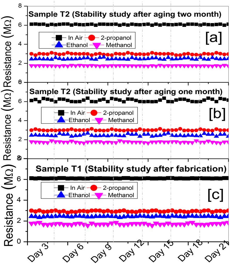 | ||
| Fig. 4 Stability study in air, 100 ppm of methanol, ethanol and 2-propanol for the sample (a) T1 (no aging), (b) T2 (one month of aging after fabrication), and (c) T3 (two months of aging after fabrication). | ||
The effect of relative humidity (RH) on the device sensing performance was investigated at room temperature under 65% RH and 90% RH. The device was exposed to 100 ppm of the alcohols in combination with 65% RH and 90% RH for the Vds of 1 V and Vgs of 1.5 V. The device responses towards 100 ppm of methanol, ethanol and 2-propanol in combination with 65% RH were found to be 73%, 62.4% and 54%, respectively. Whereas, towards 100 ppm of methanol, ethanol and 2-propanol mixed with 90% RH, the responses were 73.2%, 62.7% and 55.5%, respectively. It is worth mentioning at lower relative humidity (65% RH), the variation in sensor response was possibly due to the adsorption of water molecules on the TiO2 surfaces, and the subsequent dissociation of the same at the active site possibly helps to accumulate dipoles (OH−) and mobile protons (H+). The formation of such dipole (hydroxyl ions) and mobile protons increases the electron concentrations in the TiO2 layer. This process decreases the depletion width (λd), which thereby reduces the sensor baseline resistance.44 The deviation in response magnitude under relative humidity with respect to dry air was found to be ±8.82%. Further, we also studied the alcohol sensitivity of the present device at higher temperatures to observe the maximum achievable sensor response. The maximum sensor responses of 86%, 79% and 74% towards methanol, ethanol and 2-propanol were obtained at 250 °C.
Selectivity is the prominent parameter to determine the sensing capabilities of the device. To investigate the selectivity, the sensor device was exposed to 100 ppm of methanol, ethanol, 2-propanol, acetone, benzene, toluene and xylene at room temperature. As revealed in Fig. 5, the device showed the maximum response towards methanol among the tested gases. The responses of the device towards methanol, ethanol, 2-propanol, acetone, benzene, toluene and xylene were found to be 71%, 60%, 51%, 23%, 20%, 16% and 13%, respectively. The higher selectivity towards methanol was probably attributed to the lower molecular weight and lower carbon chain length, which facilitate the easy binding with the TiO2 thin film.45 The polarity of the alcohols decreases as the carbon chain length increases. Also, with increasing molecular size, it might not be easy to reach the active sites of the nanostructured thin film but methanol can easily bind to their surface due to the smaller molecular size and greater polarity than ethanol as well as 2-propanol. These two effects indicate a greater sensitivity towards methanol.45
 | ||
| Fig. 5 Selectivity study on the TiO2 thin film-based TFT gas sensor at room temperature. | ||
5. The role of surface states in the sensing mechanism
The positive potential above the threshold voltage forms strong conduction channels through the accumulation of majority charge carriers near the oxide and TiO2 interfaces.32 Such a gate potential is possibly the reason for charge carrier separation at the semiconducting layer. The TFT structure and its equivalent capacitance model, energy band diagram and electron flow mechanism are pictorially shown in Fig. 6(a)–(f). The chemisorption of air with subsequent carrier exchange is shown in Fig. 6(a), and the same is shown in Fig. 6(b) for methanol exposure. Fig. 6(c) shows that energy bands are flat in ideal conditions, i.e. for Vgs = 0 V. Fig. 6(d) reveals (when Vgs>Vth) electron accumulation at the SiO2–TiO2 interface, which causes bands to bend downwards. It is worth noting that in Fig. 6(d), band bending is more effective in methanol exposure (solid line) than that in air (dotted line). Such a phenomenon is attributed to the following: (i) as VGS> Vth, the accumulation of delocalized electrons near the SiO2–TiO2 interface helps to form channels. (ii) The number of carriers from such channels decrease (keeping VGS> Vth) when the device is exposed to air. In air, physisorbed O2 is converted to O−, O2− and O2− by accepting channel electrons, resulting in downward band bending and an increase in channel resistivity. (iii) However, upon methanol exposure and subsequent oxidation, trapped electrons are released back into the sensing channel. The release of trapped carriers increases the total number of free carriers at the sensing channel and hence increases the conductivity of TiO2. In such conditions, the positive potential at the drain terminal (VDS > 0) causes electron injection from the source towards the drain, leading to the current conduction. Therefore, the drain current can be modulated by either changing the gate potential or increasing the test gas concentrations. One can increase Vgs up to a certain limit (in the present case 2 V); beyond that, the device enters the linear region. Further, a higher gate potential will provide the maximum drain current but at the cost of a similar heating problem to that encountered in resistive devices. On the other hand, drain current enhancement with the increase in gas concentration also has a certain limit as the gas adsorption and subsequent oxidation are surface-limited reaction mechanisms In the present study, 100 ppm is the optimum alcohol concentration for TiO2 surfaces; beyond that, the increase in adsorption scattering and the lower gas sticking coefficient (θ) cause surface saturation, leading to the constant drain current. In a nutshell, channel charge density is governed by accumulated sheet charge density, which is non-uniform throughout the channel and solely depends on the applied gate potential and amount of gas exposure. As evident in Fig. 6(a) and (b), the sensing mechanism of the present TFT device is governed by the amount of alcohol adsorption–desorption and subsequent charge transfer between the TiO2 sensing layer and alcohol molecules. The already chemisorbed surface O− reacts with alcohol molecules and produces hydrocarbon byproducts and releases surface-trapped electrons according to eqn (3). The number of released trapped electrons (shown in eqn (4)) and hence current conductivity depend on the reaction rate co-efficient (k). The release of trapped carriers will continue until an equilibrium Fermi energy is reached within the adsorption–desorption system. The sensor response formula, correlating with the number of released trapped carriers (n), available surface sites (O−) and reaction rate co-efficient kgas, is shown in eqn (5),13 where T = test alcohol molecules, m = constant, n = number of surface trapped electrons, T′ = oxidation byproducts (CO2, CO, H2O), na = number electrons in air and n = number electrons in alcohols.| T(gas) + 5Omads → T′ + ne− | (3) |
| dn/dt = kgas[Oads]m[T]m | (4) |
| RM = {Γtkgas[O−ads]m[T]m}/ng | (5) |
 | ||
| Fig. 6 A schematic of the device structure with charge transfer processes (a) in air, and (b) in gases; (c) energy band diagram in ideal flat conditions i.e. for Vgs = 0 V; (d) the corresponding energy band alignment in air and gases; (e) the capacitance model at the SiO2–TiO2 interface and (f) the carrier transport mechanism. | ||
6. Conclusion
Room temperature TiO2 thin film in the TFT configuration for alcohol sensing is presented in this paper. The chemically synthesized TiO2 thin film showed numerous pores with uneven surfaces having oxygen vacancies originating from the paucity of water in the eletrolytes. Electrical characteristics suggest the n-channel enhancement-type FET characteristics of the fabricated device as confirmed through the threshold voltage shifts towards the lower Vgs regime. The threshold voltage (Vth) was found to be 0.65 V in air and upon exposure to 100 ppm of methanol, ethanol and 2-propanol, it was shifted to 0.4 V, 0.42 V and 0.5 V, respectively. The other properties such as Ion/Ioff (103) and sub-threshold swing (3.14 mV/decade) in air indicated negligible leakage current in the device. It is worth mentioning that the drain current (Id) change was optimum for the simultaneous excitation of the gate sweep voltage and exposure to VOCs. Such drain current fluctuation is correlated with the carrier trapping-detrapping phenomena and carrier density at the sensing channel. However, the device was found to be more sensitive to methanol among the tested gases and their response magnitudes were in the order of methanol (71%) > ethanol (60%) > 2-propanol (51%) at 100 ppm concentration. In addition, the minimum response variation under a humid environment, and better long-term stability with room temperature alcohol sensing capability of the present device pave the way for the application of the sensor in harsh environments.Author contributions
Both authors equally contributed.Conflicts of interest
There are no conflicts to declare.Acknowledgements
A part of the work is supported by Ministry of Micro, Small & Medium Enterprises (MSME), Government of India, IDEA Heckathan 2022, Project ref No. IDEAJH003262.References
- L. Jun, Q. Chen, W. Fu, Y. Yang, W. Zhu and J. Zhang, ACS Appl. Mater. Interfaces, 2020, 12, 38425–38434 CrossRef PubMed.
- I. Gawri, R. Ridhi, K. P. Singh and S. K. Tripathi, Mater. Res. Express, 2018, 5, 025303–025326 CrossRef.
- H. S. Jeong, M. J. Park, S. H. Kwon, H. J. Joo and H. I. Kwon, Sens. Actuators, B, 2019, 288, 625–633 CrossRef CAS.
- P. Lienerth, S. Fall, P. Lévêque, U. Soysal and T. Heiser, Sens. Actuators, B, 2016, 225, 90–95 CrossRef CAS.
- S. Zhao, K. O. S. Johnny, B. Xu, M. Zhao, Z. Peng and H. Cai, Sens. Actuators, B, 2000, 64, 83–87 CrossRef CAS.
- M. Jang, J. Lee, S. Y. Park, J. Lee, K. M. Lee, W. Song, S. Myung, S. S. Lee, H. K. Jung, Y. C. Kang, S. K. Kwak and K. S. An, Appl. Surf. Sci., 2021, 542, 148704 CrossRef CAS.
- J. K. Abraham, B. Philip, A. Witchurch, V. K. Varadan and C. C. Reddy, Smart Mater. Struct., 2004, 13, 1045–1049 CrossRef CAS.
- B. Liu, A. Libanori, Y. Zhou, X. Xiao, G. Xie, X. Zhao, Y. Su, S. Wang, Z. Yuan, Z. Duan, J. Liang, Y. Jiang, H. Tai and J. Chen, ACS Appl. Mater. Interfaces, 2022, 14, 7301–7310 CrossRef CAS PubMed.
- Md. A. H. Khan, R. Debnath, A. Motayed and M. V. Rao, Sensors, 2021, 21, 624–630 CrossRef CAS PubMed.
- M. Seetha and D. Mangalaraj, Appl. Phys. A: Mater. Sci. Process., 2012, 106, 137–143 CrossRef CAS.
- X. Tian, X. Cui, T. Lai, J. Ren, Z. Yang, M. Xiao, B. Wang, X. Xiao and Y. Wang, Nano Mater. Sci., 2021, 3, 390–403 CrossRef CAS.
- K. Shingange, H. C. Swart and G. H. Mhlongo, Sens. Actuators, B, 2020, 308, 127670–127681 CrossRef CAS.
- B. Bhowmik and P. Bhattacharyya, RSC Adv., 2015, 5, 82159–82168 RSC.
- S. Z. Ajabshir, E. Shafaati and A. Bahrami, Ceram. Int., 2022, 48, 24695–24705 CrossRef.
- S. Z. Ajabshir, M. S. Morassaei and M. S. Niasari, J. Colloid Interface Sci., 2017, 497, 298–308 CrossRef PubMed.
- S. Z. Ajabshir and M. S. Niasari, J. Mol. Liq., 2016, 216, 545–551 CrossRef.
- S. Z. Ajabshir and M. S. Niasari, New J. Chem., 2015, 39, 3948–3955 RSC.
- S. M. Derazkola, S. Z. Ajabshir and M. S. Niasari, J. Mater. Sci.: Mater. Electron., 2015, 26, 5658–5667 CrossRef.
- W. Ponhan, S. Phadungdhitidhada and S. Choopun, Mater. Today: Proc., 2017, 4, 6342–6348 Search PubMed.
- B. Bhowmik, J. Electron. Mater., 2019, 48, 7292–7301 CrossRef CAS.
- A. Saha, A. Moya, A. Kahnt, D. Iglesias, S. Marchesan, R. Wannemacher, M. Prato, J. J. Vilatela and D. M. Guldi, Nanoscale, 2017, 9, 7911–7921 RSC.
- Y. Su, G. Chen, C. Chen, Q. Gong, G. Xie, M. Yao, H. Tai, Y. Jiang and J. Chen, Adv. Mater., 2021, 2101262–2101283 CrossRef CAS PubMed.
- Y. Su, W. Li, L. Yuan, C. Chen, H. Pan, G. Xie, G. Conta, S. Ferrier, X. Zhao, G. Chen, H. Tai, Y. Jiang and J. Chen, Nano Energy, 2021, 89, 106321–106329 CrossRef CAS.
- C. Chen, M. Jiang, X. Luo, H. Tai, Y. Jiang, M. Yang, G. Xie and Y. Su, Sens. Actuators, B, 2022, 370, 132441–132448 CrossRef CAS.
- S. A. H. Asil, S. Z. Ajabshir, H. A. Alshamsi, A. A. Nayili, Q. A. Yousif and M. S. Niasari, Int. J. Hydrogen Energy, 2022, 47, 16852–16861 CrossRef.
- M. Yang, C. Au, G. Deng, S. Mathur, Q. Huang, X. Luo, G. Xie, H. Tai, Y. Jiang, C. Chen, Z. Cui, X. Liu, C. He, Y. Su and J. Chen, ACS Appl. Mater. Interfaces, 2021, 13, 52850–52860 CrossRef CAS PubMed.
- A. Zonarsaghar, M. M. Kamazani and S. Z. Ajabshir, Int. J. Hydrogen Energy, 2022, 47, 5403–5417 CrossRef CAS.
- S. Z. Ajabshir, M. Emsaki and G. Hosseinzadeh, J. Colloid Interface Sci., 2022, 619, 1–13 CrossRef PubMed.
- S. Z. Ajabshir, S. A. H. Asil and M. S. Niasari, Sep. Purif. Technol., 2021, 267, 118667–118679 CrossRef.
- N. K. Chowdhury and B. Bhowmik, Nanoscale Adv., 2021, 3, 73–93 RSC.
- A. K. Singh and B. Bhowmik, Nanotechnology, 2022, 33, 435501–435511 CrossRef PubMed.
- E. Wongrat, W. Ponhan and S. Choopun, Ceram. Int., 2017, 43, S520–S524 CrossRef CAS.
- S. Dutta and A. Dodabalapur, Sens. Actuators, B, 2009, 143, 50–55 CrossRef.
- C. T. Lee and P. Chou, IEEE Sens. Lett., 2018, 2, 1–3 Search PubMed.
- B. Chen, H. Liu, X. Li, C. Lu, Y. Ding and B. Lu, Appl. Surf. Sci., 2012, 258, 1971–1975 CrossRef CAS.
- P. P. Sahay and R. K. Nath, Sens. Actuators, B, 2008, 134, 654–659 CrossRef CAS.
- L. Torsi, M. C. Tanese, N. Cioffia, M. C. Gallazzi, L. Sabbatini and P. G. Zambonina, Sens. Actuators, B, 2004, 98, 204–207 CrossRef CAS.
- H. E. Swanson, H. F. McMurdie, M. C. Morris and E. H. Evans, Standard X-ray Diffraction Powder Patterns, 1966, vol. 25, pp. 82–83 Search PubMed.
- S. Z. Ajabshira, M. S. Morassaeib, O. Amiric, M. S. Niasarib and L. K. Foong, Ceram. Int., 2020, 46, 17186–17196 CrossRef.
- S. Moshtaghi, S. Z. Ajabshir and M. S. Niasari, J. Mater. Sci.: Mater. Electron., 2016, 27, 425–435 CrossRef CAS.
- B. Bhowmik and P. Bhattacharyya, IEEE Trans. Electron Devices, 2017, 64, 2357–2363 CAS.
- S. A. Nasser, Appl. Surf. Sci., 2000, 157, 14–22 CrossRef CAS.
- W. Park, J. S. Kim, G. C. Yi, M. H. Bae and H. J. Lee, Appl. Phys. Lett., 2004, 85, 5052–5054 CrossRef CAS.
- B. Bhowmik and P. Bhattacharyya, IEEE Trans. Nanotechnol., 2017, 16, 180–188 CAS.
- A. Bora, K. Mohan, D. Pegu, C. B. Gohain and S. K. Dolui, Sens. Actuators, B, 2017, 253, 977–986 CrossRef CAS.
- M. T. Vijjapu, S. G. Surya, S. Yuvaraja, X. Zhang, H. N. Alshareef and K. N. Salama, ACS Sens., 2020, 5, 984–993 CrossRef CAS PubMed.
- A. Hazra, P. P. Chattopadhyay and P. Bhattacharyya, IEEE Electron Device Lett., 2015, 36, 505–507 CAS.
- T. Ishihara, S. Sato and Y. Takita, Sens. Actuators, B, 1996, 30, 43–45 CrossRef CAS.
| This journal is © The Royal Society of Chemistry 2023 |