DOI:
10.1039/D3SC01919E
(Edge Article)
Chem. Sci., 2023,
14, 9770-9779
Transition from Dion–Jacobson hybrid layered double perovskites to 1D perovskites for ultraviolet to visible photodetection†
Received
13th April 2023
, Accepted 19th August 2023
First published on 22nd August 2023
Abstract
New perovskite phases having diverse optoelectronic properties are the need of the hour. We present five variations of R2AgM(III)X8, where R = NH3C4H8NH3 (4N4) or NH3C6H12NH3 (6N6); M(III) = Bi3+ or Sb3+; and X = Br− or I−, by tuning the composition of (4N4)2AgBiBr8, a structurally rich hybrid layered double perovskite (HLDP). (4N4)2AgBiBr8, (4N4)2AgSbBr8, and (6N6)2AgBiBr8 crystallize as Dion–Jacobson (DJ) HLDPs, whereas 1D (6N6)SbBr5, (4N4)–BiI and (4N4)–SbI have trans-connected chains by corner-shared octahedra. Ag+ stays out of the 1D lattice either when SbBr63− distortion is high or if Ag+ needs to octahedrally coordinate with I−. Band structure calculations show a direct bandgap for all the bromide phases except (6N6)2AgBiBr8. (4N4)2AgBiBr8 with lower octahedral tilt shows a maximum UV responsivity of 18.8 ± 0.2 A W−1 and external quantum efficiency (EQE) of 6360 ± 58%, at 2.5 V. When self-powered (0 V), (4N4)–SbI has the best responsivity of 11.7 ± 0.2 mA W−1 under 485 nm visible light, with fast photoresponse ≤100 ms.
Introduction
In the search for next-generation photoabsorbers for optoelectronics and photovoltaics, halide perovskites have garnered maximum interest, owing to the unwavering discovery of new phases with varying dimensionalities.1,2 Slowly but steadily, the shift in focus has been towards lead-free systems having improved moisture and thermodynamic stabilities, but with an out-of-the-common lead-perovskite-like defect tolerance.3 In this context, double perovskites with a general formula A2M(I)M(III)X6 [Pb2+ replaced by the combination of monovalent, M(I), and trivalent, M(III), cations, A = methyl ammonium (MA+), formamidinium (FA+) and/or Cs+, and X = Cl−, Br− or I−] are more benign having better stability. More than 100 double perovskites having an assorted combination of A, M(I), M(III) and X were predicted to be thermodynamically stable in terms of their structural tolerance and octahedral factor.4,5 Among them, Cs2AgBiBr6 has established itself as a benchmark lead-free double perovskite due to its similar 3D structure to Pb-containing systems, along with high carrier mobility and lifetime, low effective carrier mass, and thermodynamic stability.6,7 Nevertheless, because of the contributions of Ag+ and Bi3+ orbitals at the band edge position, Cs2AgBiBr6 has an indirect bandgap which limits its optoelectronic applications.4
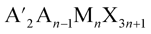
An indirect to direct bandgap transition can be made possible by the dimensional reduction of 3D double perovskites to generate HLDPs.8 The 2D modification is achieved by introducing bulky monoammonium or diammonium cations between inorganic layers, especially for a single-layered inorganic framework (n = 1), where a direct bandgap results from the contribution of single metal orbitals to the valence band maxima (VBM; Bi p-orbital) and conduction band minima (CBM; Ag d-orbital) of double perovskites.9 To date, about 40 HLDPs have been synthesized with various compositions of M(I) and M(III), and among them, (BA)4AgBiBr8 and (BA)2CsAgBiBr7 (BA = butyl ammonium cation) are the first reported HLDP structures with n = 1 and 2, having direct and indirect bandgaps, respectively.9 Most of them exist in the Ruddlesden–Popper (RP) phase and a few adopt the DJ structure. RP and DJ phases have the generalized formulae 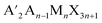 and A′′An−1MnX3n+1, respectively, where A′ is monovalent and A′′ is a bivalent bulky organic spacer cation, A is a smaller monovalent cation, M is a divalent metal or a combination of monovalent and trivalent metals, n is the number of inorganic layers and X is the halide. Accompanied by strong hydrogen bonding between the inorganic layers and diammonium spacer,10 although DJ-HLDPs have the advantages of a more stable structure and better charge transport over RP-HLDPs, containing an insulating van der Waals gap, very few reports of DJ-HLDPs are available. Among the few examples, (BDA)2AgBiBr8 (BDA = 1,4 diammonium butane) and (C8H22N2)2AgMBr8 (M = In3+, Sb3+ and Bi3+) having direct bandgaps were synthesized by the incorporation of a single layer of C4H14N2 and C8H22N2, between the monolayers of inorganic frameworks (n = 1), respectively.8,11 Nonetheless, a wide variety of DJ-HLDPs with an advantageous direct bandgap can be achieved by varying metal centers, halide composition and spacer chain lengths, an approach which is not so prevalent in the literature.12,13 While RP-HLDPs are known as photoabsorbers in only very few reports,13–16 DJ-HLDPs remain unexplored as photodetectors.
We have prepared a series of DJ-HLDPs [R2M(I)M(III)Br8; where R = NH3C4H8NH3 (4N4 = BDA) or NH3C6H12NH3 (6N6); M(I) = Ag+; M(III) = Bi3+ or Sb3+] by the acid precipitation method under ambient conditions, and the structures were elucidated by single crystal X-ray diffraction (SCXRD). The bromide HLDP crystals adapt the DJ-layered structure except when Ag+ is expelled from the 1D lattice of (6N6)SbBr5, which is formed by the simultaneous replacement of the 4N4 spacer and Bi3+ cation with the 6N6 and Sb3+ species. Moreover, when Br− is replaced by I−, the iodide containing 1D lattices of (4N4)–BiI and (4N4)–SbI are obtained, which are also bereft of Ag+. In the 1D structures, M(III)X63− (X = Br−, I−) octahedra are connected through corner shared halide ions without any chance of a larger Ag+ (rAg+ = 1.15 Å) being accommodated in the octahedra alongside Bi3+ (rBi3+ = 1.03 Å) and Sb3+ (rSb3+ = 0.76 Å). All the HLDPs show excellent thermal stability and optical density in the UV region. The band structure calculations, corroborated by the experimental results, demonstrate the actual bandgap (direct or indirect) of the HLDP and 1D perovskites, with the promise of their optoelectronic applications.
The structural dimensionality and octahedral distortions of the DJ-HLDPs and 1D perovskites have a direct correspondence with photodetection parameters. The out-of-plane photodetectors with (4N4)2AgBiBr8, having an ordered 2D lattice, show a maximum responsivity of 18.8 ± 0.2 A W−1 at 2.5 V under UV (370 nm) illumination, which overshadows all the known HLDP and most of the double perovskite photodetectors. On the other hand, the 1D phases of (4N4)–BiI and (4N4)–SbI possess a much greater absorption width as compared to the bromide HLDPs which results in better photodetection ability under self-powered conditions (0 V) both in the UV and visible ranges.
Results and discussion
Crystal structures of the DJ-HLDPs and 1D perovskites
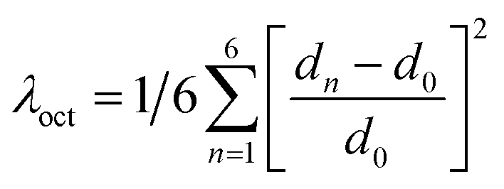
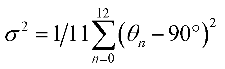
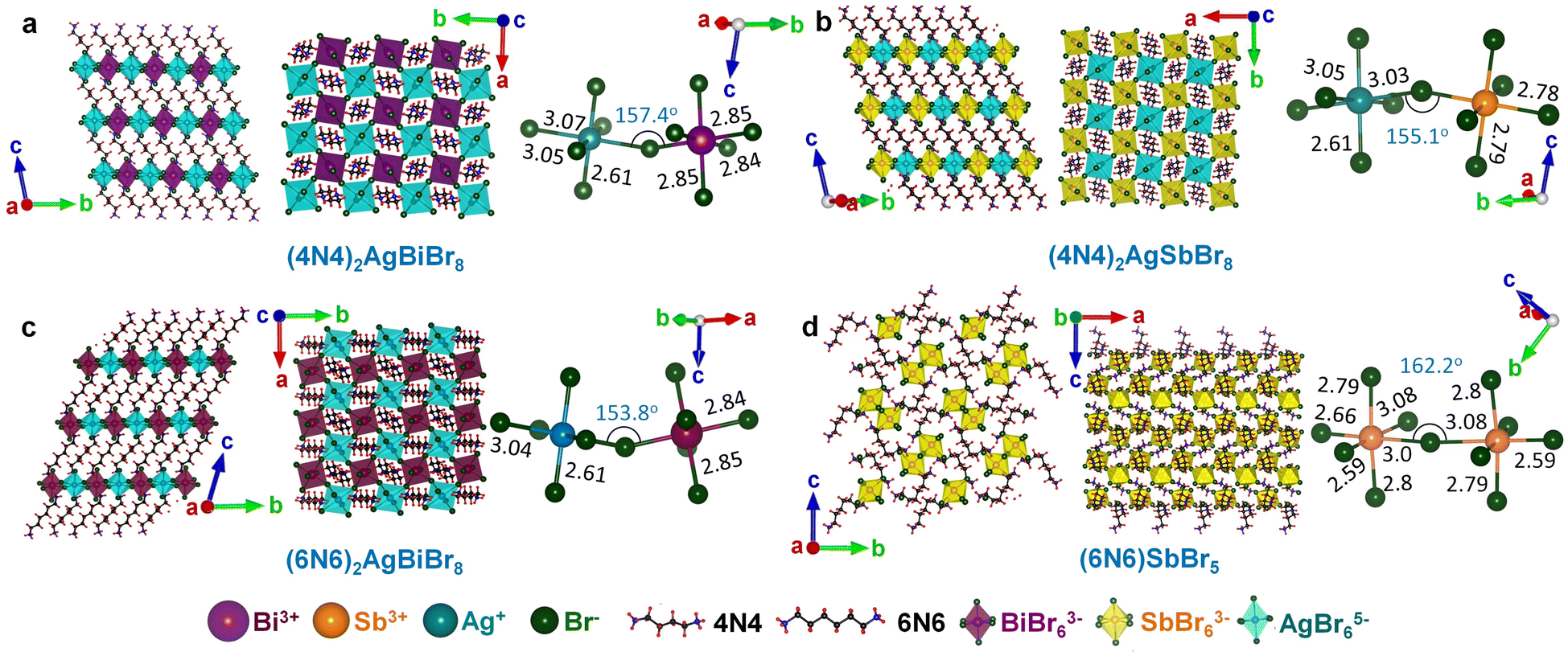
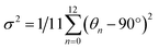
The structure of a double perovskite evolves into a DJ-HLDP by introducing a diammonium cation in between the inorganic layers, and the transformation from a DJ-HLDP into a 1D perovskite is governed by multiple factors such as introducing a bulkier spacer and octahedral tilting to prevent the entry of a larger cation (Fig. S1†). Fig. 1 presents the crystal structures of the 2D and 1D perovskites, elucidated from the SCXRD data using Mo Kα radiation. Fig. 1a and b show the structures of (4N4)2AgBiBr8 (reproduced)8 and (4N4)2AgSbBr8 along with the corresponding bond lengths and bond angles. Both these DJ-HLDPs consist of the P![[1 with combining macron]](https://www.rsc.org/images/entities/char_0031_0304.gif) space group of the triclinic system (Table 1). The inorganic layers of the yellow-colored DJ-HLDP crystals consist of the alternating corner-shared octahedra of AgBr65− and BiBr63−/SbBr63− for (4N4)2AgBiBr8 and (4N4)2AgSbBr8, respectively. The inorganic layers are separated by a single layer of the 4N4 spacer, confirming the formation of the 〈100〉 oriented DJ perovskites (Table 1). Relatively uniform M–Br bond distances are observed in BiBr63− (2.84–2.85 Å) and SbBr63− (2.78–2.79 Å) octahedra (Fig. 1a and b). A significant deviation of the Ag–Br distances especially contraction of the axial Ag–Br bond is observed in AgBr65− in both (4N4)2AgBiBr8 (Ag–Br = 2.61–3.07 Å) and (4N4)2AgSbBr8 (Ag–Br = 2.61–3.05 Å), that results in octahedral tilting and distortion. The greater ∠Bi–Br–Ag of 157.4° in (4N4)2AgBiBr8 provides a lower degree of octahedral tilting, and lower strain, as compared to ∠Sb–Br–Ag of 155.1° in (4N4)2AgSbBr8. The degree of octahedral distortion can be elucidated from the elongation factors (λoct and σ2) according to eqn (1) and (2):10
space group of the triclinic system (Table 1). The inorganic layers of the yellow-colored DJ-HLDP crystals consist of the alternating corner-shared octahedra of AgBr65− and BiBr63−/SbBr63− for (4N4)2AgBiBr8 and (4N4)2AgSbBr8, respectively. The inorganic layers are separated by a single layer of the 4N4 spacer, confirming the formation of the 〈100〉 oriented DJ perovskites (Table 1). Relatively uniform M–Br bond distances are observed in BiBr63− (2.84–2.85 Å) and SbBr63− (2.78–2.79 Å) octahedra (Fig. 1a and b). A significant deviation of the Ag–Br distances especially contraction of the axial Ag–Br bond is observed in AgBr65− in both (4N4)2AgBiBr8 (Ag–Br = 2.61–3.07 Å) and (4N4)2AgSbBr8 (Ag–Br = 2.61–3.05 Å), that results in octahedral tilting and distortion. The greater ∠Bi–Br–Ag of 157.4° in (4N4)2AgBiBr8 provides a lower degree of octahedral tilting, and lower strain, as compared to ∠Sb–Br–Ag of 155.1° in (4N4)2AgSbBr8. The degree of octahedral distortion can be elucidated from the elongation factors (λoct and σ2) according to eqn (1) and (2):10| | 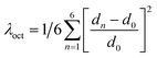 | (1) |
| |  | (2) |
where dn stands for the six M–Br bond lengths, d0 is the average M–Br bond length and θn is each ∠Br–M–Br bond angle (M = Ag+, Bi3+ and Sb3+). Due to the greater elongation factors (λoct and σ2), AgBr65− undergoes more distortion than SbBr63− or BiBr63− (Table S1†). Again, SbBr63− is more distorted than BiBr63−, implying increased octahedral distortion in (4N4)2AgSbBr8.
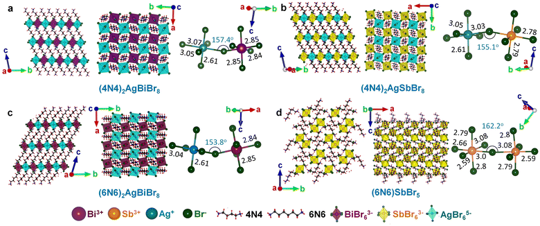 |
| | Fig. 1 Crystal structures along the a- and c-axes, with the bond lengths and angles for (a) (4N4)2AgBiBr8 (reproduced), (b) (4N4)2AgSbBr8, (c) (6N6)2AgBiBr8, and (d) (6N6)SbBr5. All bond lengths are in Å. | |
Table 1 Crystal data and structure refined data for (4N4)2AgBiBr8 (reproduced), (4N4)2AgSbBr8, (6N6)2AgBiBr8 and (6N6)SbBr5
| DJ-HLDP |
1D perovskite |
| Empirical formula |
(4N4)2AgBiBr8 |
(4N4)2AgSbBr8 |
(6N6)2AgBiBr8 |
(6N6)SbBr5 |
| Crystal system |
Triclinic |
Triclinic |
Triclinic |
Orthorhombic |
| Space group |
P |
P |
P |
P212121 |
| Unit cell dimensions |
|
a (Å) |
8.1078(2) |
8.0594(3) |
7.9577(3) |
8.1018(3) |
|
α (°) |
101.157(2) |
101.514(2) |
72.473(5) |
90 |
|
b (Å) |
8.2497(2) |
8.1066(2) |
8.2842(4) |
8.1066(2) |
|
β (°) |
92.086(2) |
91.816(3) |
82.030(4) |
90 |
|
c (Å) |
9.6870(2) |
9.6165(3) |
11.9964(7) |
14.4748(3) |
|
γ (°) |
90.386(2) |
90.723(2) |
90.3960(10) |
90 |
| Volume (Å3) |
635.20(3) |
615.22(3) |
746.42(7) |
1570.79(7) |
|
Z
|
1 |
1 |
2 |
4 |
| Density (calc.) (g cm−3) |
2.97 |
2.83 |
2.65 |
2.70 |
|
F(000) |
514 |
482 |
546.0 |
1176 |
|
θ Range for data collection (°) |
2.144–27.074° |
2.510–27.019° |
2.580–27.005° |
2.072–27.019 |
| Index ranges |
−10 ≤ h ≤ 10 |
−10 ≤ h ≤ 10 |
−10 ≤ h ≤ 10 |
−10 ≤ h ≤ 10 |
| −10 ≤ k ≤ 10 |
−10 ≤ k ≤ 10 |
−10 ≤ k ≤ 10 |
−16 ≤ k ≤ 16 |
| −12 ≤ l ≤ 12 |
−12 ≤ l ≤ 12 |
−15 ≤ l ≤ 15 |
−18 ≤ l ≤ 18 |
| Reflections collected |
22![[thin space (1/6-em)]](https://www.rsc.org/images/entities/char_2009.gif) 089 089 |
16431 |
24375 |
16537 |
| Independent reflections |
2723 [Rint = 0.1670] |
2604 [Rint = 0.1846] |
3142 [Rint = 0.1349] |
3233 [Rint = 0.0976] |
| Completeness (%) |
97 |
96.4 |
96.2 |
94 |
| Refinement method |
Full-matrix least-squares on F2 |
| Final R indices |
R
obs = 0.0698 |
R
obs = 0.0628 |
R
obs = 0.0877 |
R
obs = 0.0582 |
| [I > 2σ(I)] |
wR
obs = 0.1984 |
wR
obs = 0.1529 |
wR
obs = 0.2209 |
wR
obs = 0.1217 |
| Largest diff. peak and hole (e Å−3) |
7.24 and −5.75 |
2.71 and −2.63 |
8.9 and −2.8 |
1.3 and −1.7 |
| GOF |
1.042 |
1.058 |
1.161 |
1.037 |
With a 6-C spacer, the DJ-HLDP structure of (6N6)2AgBiBr8 has a similar P space group, with alternating corner-shared AgBr65− and BiBr63− in the inorganic layers, separated by a single 6N6 molecule (Fig. 1c and Table 1). Upon increasing the spacer chain length from 4N4 to 6N6, the ∠Bi–Br–Ag decreases to 153.8° and the octahedral tilting increases. However, for the Sb counterpart, Ag+ cannot be incorporated into the (6N6)SbBr5 lattice due to the already existing substantial distortion in SbBr63− with large elongation factors and increased axial and equatorial bond length variations (Fig. 1d and Tables 1 and S1†). If Ag+ could have been inserted alongside Sb3+, the AgBr65− moiety would have undergone further distortion, and the lattice would have been unfavorably contorted. In the absence of Ag+, the corner-shared SbBr63− octahedra form a 1D structure having a lower degree of octahedral tilting with ∠Sb–Br–Sb of 162.2° and lower lattice strain. Unlike the 2D HLDPs, (6N6)SbBr5 crystallizes in the orthorhombic system with space group P212121. With a single corner shared SbBr63− entity and having a different space group, (6N6)SbBr5 is less strained than the HLDP structures containing two different octahedra, AgBr65− and BiBr63− or SbBr63−. The powder XRD (PXRD) patterns of all the above perovskites match the simulated results obtained from the SCXRD data (Fig. S2†). In the PXRD patterns, some less intense reflections are additionally observed at 2θ > 20°, since the powders obtained by grinding the single crystals expose a few extra planes to the incident X-ray beam.
Physicochemical characterization
The elemental mapping with high-angle annular dark field scanning TEM (HAADF-STEM) clearly shows the elemental stoichiometry, the presence of Ag+ in the DJ-HLDP structures and its absence in the 1D perovskite system of (6N6)SbBr5 and iodides of HLDPs (Fig. S3 and Table S2†). The iodides do not contain Ag+ due to the formation of 1D structures as a result of the tendency of Bi3+ and Sb3+ to form low-dimensional non-perovskite phases and the reluctance of Ag+ to form octahedral coordination with I−.17,18 As a result, the iodide analogues of (4N4)2AgBiBr8 and (4N4)2AgSbBr8 are termed (4N4)–BiI and (4N4)–SbI, respectively. The iodides form 1D crystal structures with formula A′′BI5 (A′′ = diammonium cation, B = Bi3+ or Sb3+), consisting of the corner shared BI63− octahedra in a particular direction forming trans-connected 1D chains,19,20 similar to (6N6)SbBr5 (Fig. 1d). In fact, inductively coupled plasma-mass spectrometry (ICP-MS) analysis of the supernatant in the reaction media synergistically shows the non-inclusion of silver in the solid products of the 1D perovskite. When Ag+ is not included in the (6N6)SbBr5 lattice, the supernatant contains a higher stoichiometric amount of 2.1 at% silver than 0.2 at% when Ag + could be inserted in the (4N4)AgBiBr8 lattice. The X-ray photoelectron spectral (XPS) survey scan of the bromide systems likewise shows the absence of a Ag 3d signal in (6N6)SbBr5 (Fig. S4†). To verify the thermal stability of these perovskites under ambient conditions, thermogravimetric analysis (TGA) was carried out (Fig. S5†). (4N4)2AgBiBr8 decomposes above 300 °C and is more stable than (4N4)2AgSbBr8, which decomposes at 230 °C. On the other hand, (6N6)2AgBiBr8 is more stable than (6N6)SbBr5, most likely due to the lower BiBr63− octahedral distortion in DJ-HLDP than the distortion of SbBr63− in the 1D perovskite.
The more halide vacancies and octahedral distortion, the larger the fraction of lower oxidation states of the cations. The XPS data from the Bi 4f level of (4N4)2AgBiBr8 indicate 6% lower oxidation states of Bi(3−x)+ alongside Bi3+, because of the halide vacancies (Fig. S6 and Table S3†). Since AgBr65− undergoes more octahedral distortion, the Ag 3d level exhibits 7.6% lower oxidation states of Ag(1−x)+. Also, the deconvoluted peaks of the N 1s level show a small fraction of the non-protonated amine and a more than 9 times higher fraction of its pronated counterpart at a higher binding energy of 401.9 eV (Fig. S6d and Table S3†). (4N4)2AgSbBr8 exhibits similar XPS results but because of a larger octahedral distortion and higher halide vacancy (Table S1†), the fraction of lower oxidation states is more, 7.4% for both Sb(3−x)+ and Ag(1−x)+ (Fig. S7 and Table S3†). On the other hand, an analysis of the Bi 4f and Ag 3d levels of (6N6)2AgBiBr8 shows the presence of 13.4 and 14.1% lower oxidation states from the undercoordinated Bi and Ag, respectively, as a result of high octahedral tilting and ion migration (Fig. S8 and Table S4†).21 However, the fraction of Sb(3−x)+ is only 4.8% in (6N6)SbBr5 because of a lower octahedral tilting in the presence of a single metal (Sb).22
Optical properties.
The absorption spectra of the DJ-HLDPs show sharp absorption edges below 500 nm and the absorption edges are red-shifted from Sb3+ to Bi3+perovskites (Fig. 2a). The direct and indirect bandgap values were extracted using the Kubelka–Munk eqn (3):8| | | F(R) = α = (1 − R)2/2R | (3) |
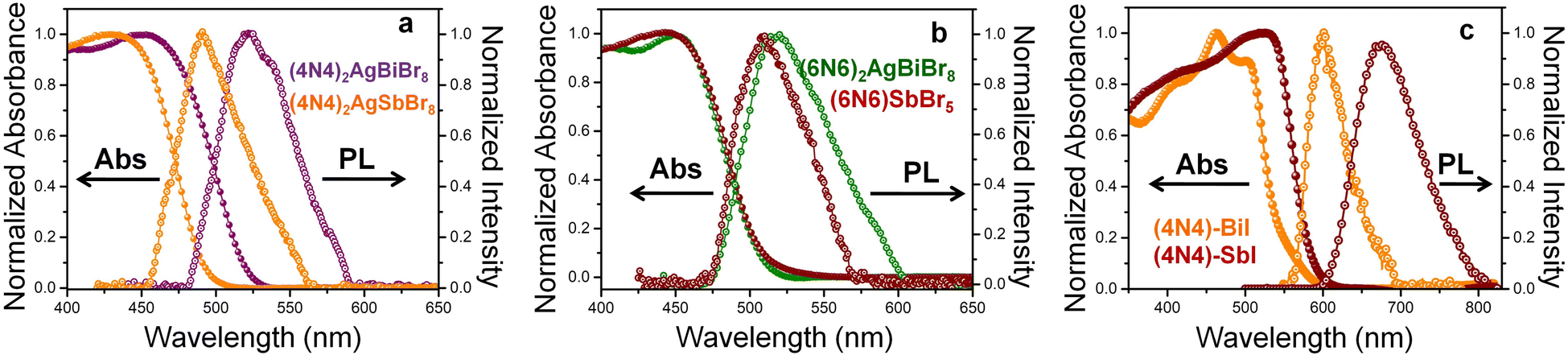
where R is the reflectance and α is the absorption coefficient. The red shift of this rich UV absorption is due to the lower bandgap for (4N4)2AgBiBr8 than for (4N4)2AgSbBr8 (Fig. S9 and Table S5†). Despite the dissimilar structures of (6N6)2AgBiBr8 2D-HLDP and (6N6)SbBr5 1D-perovskite, the absorption edges do not change much, that results in similar bandgaps (Fig. 2b). The PL emission spectra of (4N4)2AgBiBr8, (4N4)2AgSbBr8, (6N6)2AgBiBr8 and (6N6)SbBr5 exhibit band-edge emission with lower Stokes shift and FWHM (Table S5†). The PL wavelength shifts follow the absorption trends. The emission band of (6N6)2AgBiBr8 has a broader shoulder than (6N6)SbBr5, due to the presence of mid-gap states in the former. The iodide perovskites demonstrate absorption over a wide visible range, where the absorption edge of (4N4)–SbI is red-shifted more than that of (4N4)–BiI (Fig. 2c), unlike the bromide DJ-HLDPs. The iodide perovskite crystals have a bright distinct appearance, in comparison to the yellow-colored crystals of the bromide systems. The experimental bandgap of (4N4)–SbI is lower than that of (4N4)–BiI (Fig. S9†). The PL band of (4N4)–SbI is more red-shifted than (4N4)–BiI and shows a broader emission band.
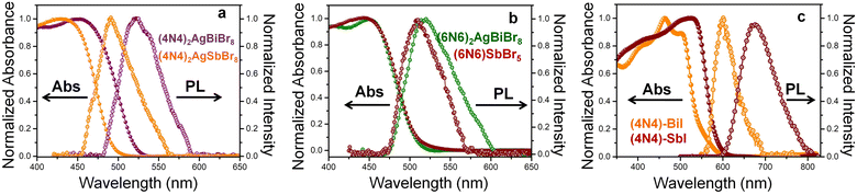 |
| | Fig. 2 Absorption and PL spectra of (a) (4N4)2AgBiBr8 and (4N4)2AgSbBr8, (b) (6N6)2AgBiBr8 and (6N6)SbBr5, and (c) (4N4)–BiI, and (4N4)–SbI. | |
The absorption spectra of the perovskite films show similar trends to the single crystals, although the PL spectra of the films are relatively weaker with a low signal-to-noise ratio (Fig. S10†). The cross-sectional microscopic view of the films reveals the presence of pinholes and grain boundaries as non-radiative recombination centers, which lowers the emission intensity (Fig. S11†). Among the bromide HLDP films, (4N4)2AgBiBr8 shows a relatively intense emission band because of its better film quality. The absorption coefficient values were estimated from the absorption and thickness of the perovskite films, which varies between 0.7 and 0.9 μm (Fig. S11†). Since, the iodide perovskites have better optical density, their absorption coefficient values are higher than their bromide counterparts (Table S6†). Among the bromide HLDPs, (4N4)AgBiBr8 exhibits the highest absorption coefficient of 8.3 × 103 cm−1 at 400 nm (near UV region), whereas (4N4)–SbI shows the overall highest absorption coefficient of 1.5 × 104 cm−1 at 470 nm (visible region).
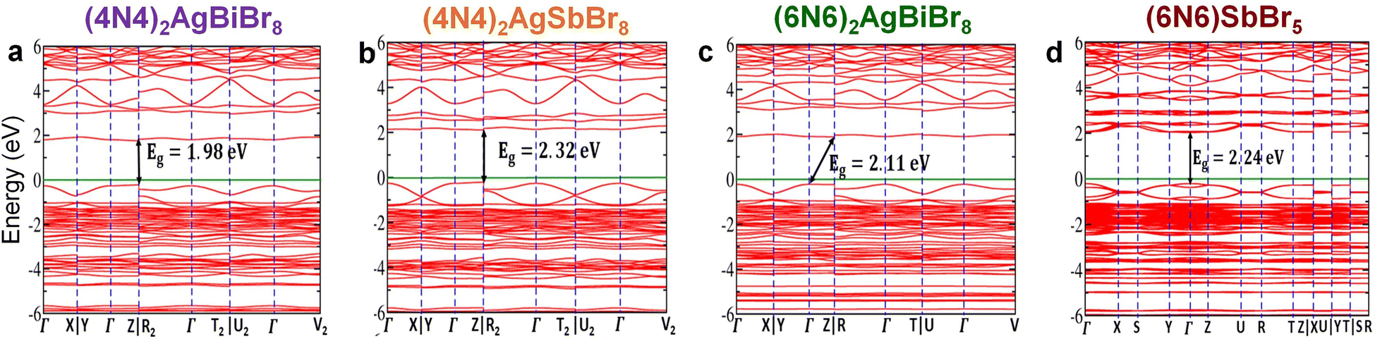
Band structure calculations.
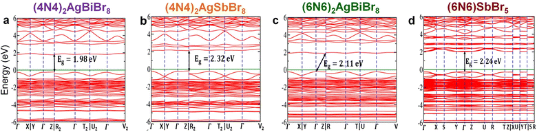
First-principles calculations have been performed to explore the band structure of the HLDPs. The band structures without the inclusion of spin–orbit coupling (SOC) show an indirect bandgap for all the structures except 1D (6N6)SbBr5 (Fig. S12†). For (4N4)2AgBiBr8, the valence band maximum (VBM) and conduction band minimum (CBM) are located at the Z and X points, respectively. Similar positions of the VBM and CBM are also observed for (4N4)2AgSbBr8, but for (6N6)2AgBiBr8, the VBM and CBM are at Γ and X points, respectively. On the other hand, (6N6)SbBr5 has the VBM and CBM both located at the Γ point and therefore shows a direct bandgap of 2.41 eV. However, after considering SOC, the band structures of (4N4)2AgBiBr8 and (4N4)2AgSbBr8 show direct bandgaps of 1.98 and 2.32 eV, respectively, where both the VBM and CBM are located at point Z (Fig. 3a and b). After applying SOC in (6N6)2AgBiBr8 the bandgap nature remains indirect but VBM and CBM positions are changed in comparison to the band without SOC. The indirect bandgap is reduced to 2.11 eV with the VBM and CBM located at Γ and R points, respectively (Fig. 3c). In the presence of SOC, (6N6)SbBr5 also exhibits a direct bandgap of 2.24 eV, where both the VBM & CBM are located at the Γ point (Fig. 3d). All the SOC calculations were performed with the PBE functional, which underestimates the bandgap due to the self-interaction error of a many-electron system. The hybrid exchange–correlation functional i.e., HSE06 or GW gives the exact bandgap like the experimental one, but these are computationally very expensive and beyond the scope of this work. However, the conclusion derived from the Perdew–Burke–Ernzerhof (PBE) level of calculations is qualitatively correct to estimate the band nature with and without SOC.9,11 Interestingly, we found that for all three HLDPs, a unique intermediate band emerges above the Fermi level, which results in bandgap reduction after applying SOC. Notably, SOC has a significant impact on the bandgap of compounds containing heavy metals (Fig. 3 and S12†) because of the larger mass and significant p-character of the metal in the conduction band.8
 |
| | Fig. 3 Electronic band structures for (a) (4N4)2AgBiBr8, (b) (4N4)2AgSbBr8, (c) (6N6)2AgBiBr8 and (d) (6N6)SbBr5. The calculations were performed with SOC and the green lines represent the Fermi energy level. | |
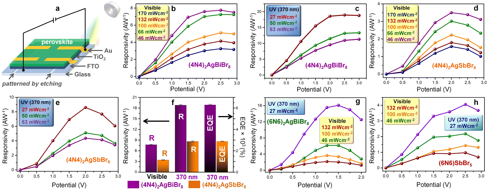
Photodetection under the applied potential bias.
The out-of-plane photodetectors consist of the DJ-HLDP films spin-coated on top of compact TiO2, the electron transport layer (ETL), deposited on the fluorine-doped tin oxide (FTO) coated glass substrate (Fig. 4a). These films demonstrate similar XRD reflections to the crystals, where the smaller number of XRD peaks resembles an ordered 2D topology (Fig. S13†). With a device structure of FTO/TiO2/perovskite/Au,23 the devices can operate both in the UV (370 nm) and visible (1 sun) regions, because of an appreciable optical density over the wide spectral range (Fig. 2a and 4). The Fermi energy levels indicate the p-type nature of the perovskites and a suitable alignment of the energy levels of the HLDP photoactive layers favors efficient carrier transport to the electrodes (Fig. S14†). The current density versus voltage (J–V) plots of (4N4)2AgBiBr8 and (4N4)2AgSbBr8 devices indicate a higher photocurrent under UV (370 nm) radiation (Fig. S15†). The current densities increase with the intensity of visible light (46–170 mW cm−2) and UV radiation (27–63 mW cm−2) (Fig. S16†). The responsivity increases with the applied bias due to the increasing difference of current density under light and dark (JL–JD) conditions as well as with the lowering of light intensity in both the spectral ranges (Fig. 4b–e). After an initial increase in responsivity up to the threshold potential, the sharp increase in JD above the threshold decreases the responsivity. In addition, at higher applied potentials, the plausible ion migration effect under illumination cannot increase the photocurrent any further which in turn affects the device performance. The photodetection ability of (4N4)2AgBiBr8 devices appears to be the best under all conditions due to a lower direct bandgap, minimized octahedral distortions, and a higher absorption width. In the presence of 27 mW cm−2 UV light, the maximum responsivities are 18.8 ± 0.2 A W−1 and 8.6 ± 0.2 A W−1 for (4N4)2AgBiBr8 and (4N4)2AgSbBr8 devices under 2.5 and 2 V applied bias, respectively (Table S7†). The EQE follows a similar trend, and the maximum EQE is found to be 6360 ± 58% at 2.5 V for (4N4)2AgBiBr8 and 2880 ± 58% at 2 V for (4N4)2AgSbBr8, under illumination of 370 nm, 27 mW cm−2 (Fig. 4f, S17a, b and Table S7†). (4N4)2AgBiBr8 also displays the highest detectivity of 1.1 (±0.02) × 109 Jones at 1.5 V in comparison to 8 (±0.02) × 108 Jones at 1.5 V for the (4N4)2AgSbBr8 devices (Fig. S17c†). Due to the sharp increase in JD with the applied potential bias, detectivity starts to decrease gradually beyond 1.5 V. The chronoamperometry plots of the (4N4)2AgBiBr8 photodetector at different potentials, from 0.05 to 1.5 V, illustrate a potential dependent gradual increase in both JD and JL under visible light, resulting in an increase of JL–JD and thereby generating higher responsivity at larger potentials (Fig. S17d and e†).
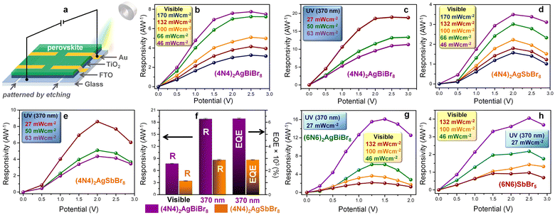 |
| | Fig. 4 Potential-biased photodetector performance. (a) Schematic of the photodetector device. Responsivity–potential plots under 1 sun visible light and 370 nm UV light for (b and c) (4N4)2AgBiBr8, and (d and e) (4N4)2AgSbBr8. (f) Bar plots of the highest responsivity and EQE under visible and UV radiation for (4N4)2AgBiBr8 and (4N4)2AgSbBr8. Responsivity–potential plots under 1 sun visible light and 370 nm UV light for (g) (6N6)2AgBiBr8 and (h) (6N6)SbBr5. | |
The (6N6)2AgBiBr8 photodetectors similarly display a higher photocurrent under UV radiation (370 nm) than under visible light illumination and an increase in JL with increasing applied potential (Fig. S15c†). On the other hand, the (6N6)SbBr5 1D perovskite records a lower photocurrent than (6N6)2AgBiBr8 (Fig. S15d†). The J–V plots of (6N6)2AgBiBr8 and (6N6)SbBr5 photodetectors exhibit a slight increase in JL with increasing visible light intensity from 66 to 132 mW cm−2 followed by a decrease in JL at 170 mW cm−2 (Fig. S18a and b†). The chronoamperometry plots of (6N6)2AgBiBr8 devices also show an increment of the (JL–JD) difference at higher applied potentials (Fig. S18c and d†). At 370 nm illumination and 27 mW cm−2 light intensity, the maximum responsivities are 16.1 ± 0.2 and 4.1 ± 0.1 A W−1 for (6N6)2AgBiBr8 and (6N6)SbBr5 devices at 1.5 and 2.5 V, respectively (Fig. 4g, h and Table S7†). Due to the sharp increase of JD beyond the threshold potential, the responsivity decreases, a trend also followed by the detectivity and EQE (Fig. 4g, h, S18e, and f†). While the highest detectivity is obtained at 1 V, (6N6)2AgBiBr8 has better photodetection parameters than (6N6)SbBr5. Under potential bias, (4N4)2AgBiBr8 demonstrates the best photodetection and (6N6)2AgBiBr8 shows a maximum detectivity of 1.9 (±0.1) × 109 Jones at 2 V due to its lower JD (Fig. S19 and Table S8†). (4N4)–BiI and (4N4)–SbI show better photocurrent in the visible region under 485 nm illumination due to their absorption in the visible spectral region (Fig. S10†), but under UV radiation, their photodetection parameters are overshadowed by those of their bromide counterparts. In the case of 485 nm illumination, the responsivity, detectivity and EQE of (4N4)–BiI are 1.6 (±0.1) A W−1, 1.3 (±0.1) × 109 Jones and 405 (±5) %, while those of (4N4)–SbI are 6.1 (±0.1) A W−1, 1.3 (±0.1) × 109 Jones and 1560 (±15) %, respectively (Fig. S20†). The visible range photoabsorption by the iodide films allows them to maintain the photodetection parameters throughout the visible spectrum with an absorption edge at 550–580 nm (Fig. S21†). The performance of 4N4–Sb–I remains always better than that of 4N4–BiI, and the highest parameters are obtained at 485 nm. In contrast, the UV absorption of the HLDP films restricts the optical measurements only to 370 nm (Fig. S10a†).
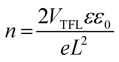
The highest photodetection parameters obtained in this work are much greater than those of reported HLDP photodetectors (Table S9†)14–16 and layered DJ perovskites (Table S10†)24–30 and comparable with those of devices based on double perovskites (Cs2AgBiBr6; Table S11†).31–35 The best performance of (4N4)2AgBiBr8 photodetectors can be explained by their low trap state density (n) and high carrier mobility (μh) in comparison to the (6N6)SbBr5 devices. The n and μh are obtained from the VTFL data of the J–V plot under dark conditions (Fig. S22a†) and the slope of the J–V2 plot (Fig. S22b†), respectively.36 The n and μh of (4N4)2AgBiBr8 devices are measured to be 1.64 × 10¹⁶ and 1.52 (±0.021) × 10−2 cm2 V−1 s−1 which are respectively much lower and higher than those of (6N6)SbBr5, having n = 1.91 × 10¹⁶ and μh = 7.71 (±0.025) × 10−3 cm2 V−1 s−1.
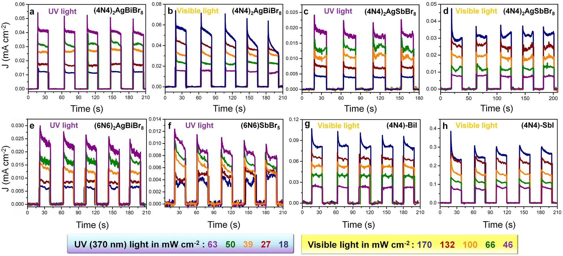
Self-powered photodetection.
In the absence of any applied potential bias (self-powered conditions), JL increases by increasing the light intensities both with visible (46–170 mW cm−2) and 370 nm UV light (18–63 mW cm−2) (Fig. 5). Although the JL of (4N4)2AgBiBr8 obtained in the visible range is higher than that obtained with UV light, the photocurrent stability is maintained only under UV light, even at higher light intensities (Fig. 5a). At 170 mW cm−2 visible light intensity, (4N4)2AgBiBr8 is likely to degrade (Fig. 5b). (4N4)2AgBiBr8 also exhibits greater JL values than (4N4)2AgSbBr8 under both visible and UV light (Fig. 5c and d), similar to that under the potential biased conditions (Fig. 4). In the self-powered mode, all the devices display the same JD values (near zero) and demonstrate fast photoresponse, which is evident from the low rise time (RT) and fall time (FT) extracted from the chronoamperometry plots under zero bias (Fig. 5a, c and Table S12†). The higher JL of (4N4)2AgBiBr8 can be explained by the lower charge transfer resistance (RCT), obtained from the Nyquist plots at 0 V under UV light (Fig. S23a†). For both the devices, RCT decreases gradually by increasing the UV light intensity, because of an increase in the corresponding photocurrent (Fig. S23a and b†). With a stepwise increase in potential, a corresponding increase in the (JL–JD) difference as well as the responsivity is obvious (Fig. S24†). Among the DJ-HLDP structures, (4N4)2AgBiBr8 achieves maximum responsivities of 0.67 and 0.36 mA W−1 under 370 nm and visible light illumination, respectively. The responsivity and detectivity of the self-powered devices remain unchanged with varying light intensities (Fig. S25† and Table S13†). With the 6-C spacer, the UV light-assisted self-powered photocurrent and responsivity are higher for (6N6)2AgBiBr8 photodetectors than for (6N6)SbBr5 (Fig. 5e, f and S26a and b†). These observations are manifested by a lower RCT for (6N6)2AgBiBr8 photodetectors (Fig. S23c and d†). The responsivity and detectivity of these self-powered devices do not show any major variation when increasing the light intensity (Fig. S26†). Considering the juxtaposed relations of R ∝ D ∝ Jph ∝ 1/IL, where Jph is the photocurrent density and IL is the light intensity, R and D remain nearly constant with increasing IL.
 |
| | Fig. 5 Self-powered photodetector performance. Chronoamperometry plots at different light intensities, for (4N4)2AgBiBr8 under (a) 370 nm UV and (b) 1 sun visible light, (4N4)2AgSbBr8 under (c) 370 nm UV and (d) 1 sun visible light, (e) (6N6)2AgBiBr8 and (f) (6N6)SbBr5, under UV light, and (g) (4N4)–BiI and (h) (4N4)–SbI in the presence of visible light. | |
Even though (4N4)2AgBiBr8 has the best photodetection parameters among the bromide perovskites (Fig. S27 and Tables S14 and S15†), the iodide perovskites perform the best in the self-powered mode, shifting the photodetection range from UV to the visible range. The photodetectors of (4N4)–SbI exhibit higher photocurrent under self-powered conditions than the (4N4)–BiI devices (Fig. 5g and h). In the case of the iodide perovskites, the photoresponse of (4N4)–SbI is higher under visible light with different intensities (46 to 170 mW cm−2), because of the larger absorption width in the visible region (Fig. 2c). (4N4)–SbI records a wavelength-dependent photoresponse, depending on its absorption range with a maximum responsivity of 11.7 mA W−1 under 485 nm illumination (Fig. S28a, b and Table S16†). In spite of (4N4)–SbI having a modest JL at 485 nm, the responsivity is higher since IL is much lower at 485 nm (4.7 mW cm−2) than at 370 nm (10.3 mW cm−2). In the visible range, (4N4)–SbI shows better performance than the champion (4N4)2AgBiBr8 (Fig. S28c; Table S16†). Both (4N4)–BiI and (4N4)–SbI show remarkable stability in terms of their photocurrent for 18 min under continuous high-intensity illumination of 170 mW cm−2 (Fig. S29†), unlike MAPbI3 or CsPbI3.37,38
Conclusions
In summary, starting from (4N4)2AgBiBr8, a series of stable lead-free DJ-HLDP phases were prepared by varying the metal sites (Bi3+ or Sb3+) and diammonium spacer cations (4N4 and 6N6). All the 〈001〉 oriented thermally stable HLDP crystals exist in 2D structures having alternating corner-shared AgBr65− and BiBr63− or SbBr63− octahedra in the inorganic layer, separated by a single layer of the organic diammonium spacer. While (4N4)2AgBiBr8, (4N4)2AgSbBr8 and (6N6)2AgBiBr8 crystallize as DJ-HLDPs, (6N6)SbBr5 exists as a 1D perovskite without any Ag+ in the crystal lattice. The iodide containing (4N4)–BiI and (4N4)–SbI also form 1D perovskites, with zig-zag chains consisting of corner-shared octahedra. The yellow-colored bromide crystals show sharp absorption edges below 500 nm with lower bandgaps for (4N4)2AgBiBr8 than for (4N4)2AgSbBr8 and the bandgap increases slightly by increasing the spacer chain length from 4N4 to 6N6. Band structure calculations show that the DJ-HLDPs exhibit direct bandgaps after considering the SOC effect, unlike the Cs2AgBiBr6 double perovskite. Among the bromide systems, the (4N4)2AgBiBr8 photodetectors demonstrate the highest UV photodetection parameters in both potential-biased and self-powered modes due to its larger absorption edges and a smaller insulating spacer (4N4) in between the inorganic layers, resulting in the lowest RCT and n and the highest μh. Since the spectral responses of the bromide HLDPs are confined within the UV region, the photoresponse is tuned towards the visible region by changing the halide composition from bromide to iodide. In the case of the iodide systems, (4N4)–BiI and (4N4)–SbI, the spectral onset appears at 580 nm and the highest photodetection at 485 nm. In self-powered mode, (4N4)–SbI has a maximum responsivity of 11.7 ± 0.2 mA W−1 under 485 nm illumination, greater than that of (4N4)2AgBiBr8 champion devices at 370 nm (0.67 ± 0.01 mA W−1), with a fast photoresponse below 100 ms.
Experimental section
Chemicals and materials
Hydrobromic acid (HBr, 48 wt% in H2O, Sigma Aldrich), bismuth bromide (BiBr3, Sigma Aldrich), silver bromide (AgBr, Sigma Aldrich), antimony trioxide (Sb2O3, SRL), 1,4 diaminobutane (NH2C4H8NH2, Sigma Aldrich), 1,6 diaminohexane (NH2C6H12NH2, Sigma Aldrich), hydroiodic acid (HI, 57 wt% in H2O, Sigma Aldrich), silver iodide (AgI, Sigma Aldrich), and hexane (Merck) were used without further purification.
Synthesis of (NH3C4H8NH3)2AgBiBr8 [(4N4)2AgBiBr8]
0.5 mM each of BiBr3 and AgBr powders were dissolved in 2 ml concentrated HBr solution under vigorous stirring at 60 °C for 15 min followed by the addition of 1 mM 1,4 diaminobutane (4N4) to the acidic solution.8 The mixture was stirred at 100 °C for 30 min to form a colorless transparent solution. After slow cooling, yellow (4N4)2AgBiBr8 crystals were obtained. The product was filtered using a Whatman filter along with multiple washings with hexane.
Synthesis of (NH3C4H8NH3)2AgSbBr8 ((4N4)2AgSbBr8)
(4N4)2AgSbBr8 crystals were synthesized by a similar acid precipitation method except that 0.25 mM Sb2O3 and 0.5 mM AgBr were dissolved in HBr solution.
Synthesis of (NH3C6H12NH3)2AgBiBr8 [(6N6)2AgBiBr8]
(6N6)2AgBiBr8 crystals were synthesized by dissolving 0.5 mM each of BiBr3 and AgBr powders in 2 ml HBr solution followed by the addition of 1 mM of 6N6. The resulting solution was stirred at 100 °C for 30 min followed by slow cooling to form yellow crystals.
Synthesis of (NH3C6H12NH3)2SbBr10 [(6N6)SbBr5]
(6N6)SbBr5 crystals were synthesized by a similar acid precipitation method except that 0.25 mM Sb2O3 and 0.5 mM AgBr were dissolved in HBr solution. Even after adding 0.5 mM AgBr along with 0.25 mM Sb2O3, Ag+ was not incorporated into the crystal structure.
Synthesis of (4N4)–BiI and (4N4)–SbI
The iodide perovskites were prepared by dissolving the same mM concentrations of Bi, Sb and Ag (not incorporated in the lattice) precursors in HI solution followed by the addition of 1 mM of 4N4 and stirring at 100 °C for 30 min to form an orange-colored clear solution. After slow cooling of the resulting solutions, orange (4N4)–BiI and deep red (4N4)–SbI crystals appeared.
Characterization
The SCXRD data were collected on a Rigaku (dual, Cu/Mo at zero Eos) diffractometer using graphite monochromated Mo Kα radiation (λ = 0.71073 Å) at a temperature of 100 K with the help of a cryojet. The SCXRD of (4N4)2AgBiBr8 was reproduced at 293 K. Using Olex2, the structures were solved with the ShelXT structure solution program using intrinsic phasing and refined with the ShelXL refinement package using least squares minimization. All non-hydrogen atoms were refined anisotropically. Three-dimensional visualization of the crystal structures was obtained using Vesta software from the cif files generated from the SCXRD results. PXRD measurements were carried out with a Rigaku X-ray diffractometer (Cu Kα irradiation, λ = 1.541 Å). The TGA analysis was performed with a PerkinElmer TGA 4000 under N2 at 10 °C min−1 from 30 to 60 °C. The ICP-MS measurements were carried out on a Thermo Scientific X-series with Plasma Lab software. The field emission scanning electron microscope (FESEM) images were taken on a Carl Zeiss SUPRA 55VP FESEM. The EDX spectra and mapping were recorded on an Oxford Instruments X-Max system with the INCA software coupled to FESEM. UV-vis absorption spectra of the solid powder samples were recorded with a Jasco V-670 spectrophotometer by preparing sample pellets and a BaSO4 bar as a reference. PL emission spectra were measured with a Horiba JobinYvon Fluorolog using a Xe lamp as the excitation source. XPS measurements were performed by mounting the sample pellets on carbon in a commercial photoelectron spectrometer PHI 5000 Versa Probe III at CRF IIT (ISM) using an Ar ion beam as the excitation source. The acquired peaks were fitted using Fityk software, with the Voigt peaks having 80% Gaussian and 20% Lorentzian components to evaluate the valence states. All of the data were corrected with respect to the C 1s spectra. For calculating the energy levels of the bromide HLDPs, cyclic voltammograms were recorded in dry acetonitrile and tetrabutylammonium hexafluorophosphate at a scan rate of 50 mV s−1 under nitrogen at room temperature. A platinum disk was used as the working electrode, platinum wire as the counter electrode and silver wire (dipped in aqueous FeCl3 prior to use) as the pseudo-reference electrode. The potential was externally calibrated after each experiment, against the ferrocene/ferrocenium couple. Ultraviolet photoelectron spectroscopy (UPS) measurements were carried out with a PHI VersaProbe 4 Scanning XPS microprobe, to calculate the Fermi energy level and energy band positions of the bromide and iodide perovskites. The samples were prepared in the form of pellets mounted on double-sided Cu conducting tape. All the experiments were performed in a vacuum and at in-ground bias in the presence of a 1 alpha excitation source (photon energy = 21.2 eV).
Computational details
All the first principles DFT computations were performed using the Vienna ab initio simulation package (VASP).39,40 The ion–electron interactions were described using the projected-augmented wave.41 The PBE functional of the generalized gradient approximation (GGA) was employed to consider the exchange–correlation energy.42 The kinetic energy cut off was set at 600 eV. We have calculated the band structure of the materials without and with SOC. All calculation steps include an energy convergence of 10−8 eV. For obtaining the optimized ground-state structure, Hellman–Feynman forces43 were converged with a limit of 0.005 eV Å−1.
Fabrication of photodetectors
For fabricating the out-of-plane photodetector devices, at first, FTO-coated glass substrates were etched with Zn powder and concentrated HCl to create a desired pattern. During the etching process, Zn powder was placed on the unmasked portion of the FTO substrate followed by the dropwise addition of concentrated HCl (38%). The FTO coating was etched out of the glass substrate to expose the pattern, confirmed by measuring the resistance with a multimeter. After patterning, the FTO substrates were washed sequentially with soap and pure water, ethanol and isopropanol by ultrasonication, 10 min for each solvent. Subsequently, a thin ETL of compact TiO2 (c-TiO2) was deposited on the patterned FTO by spin-coating an ethanolic solution of titanium isopropoxide at 4000 rpm for 30 s, followed by high-temperature annealing at 550 °C for 1 h. 200 mg ml−1 perovskite precursor solution in DMF was spin-coated on top of the ETL at 2000 rpm for 30 s followed by heat treatment for 15 min at 80 °C inside a glovebox. The deposited substrates were then transferred inside the thermal evaporator unit for the deposition of a thin Au contact electrode (∼200 nm) at the top of the perovskite layer by using a shadow mask at a deposition rate of 2 Å s−1 and base pressure of 5 × 10⁻⁶ Torr. The deposited Au film thickness was estimated in situ using a quartz crystal thickness monitor, such that the device area was kept at 0.04 cm2. Photodetector measurements were performed using a steady-state AM 1.5 G Solar Simulator Class AAA Model PEC-L01 (Batsol) equipped with a Biologic Instruments VSP-300 workstation. Since the light intensity is equivalent to the area under the counts versus wavelength curves, the visible light intensity varies from 46–170 mW cm−2 and that of UV light from 18–63 mW cm−2, although power of the light is the same in both cases. The photodetector performance was evaluated using the R, D, and EQE parameters expressed as:| | 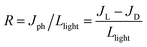 | (4) |
| | | Detectivity (D) = R/(2qJD)1/2 | (6) |
where JL and JD are current density under light and dark conditions, Llight is the incident light intensity, and c, h, λ and q are the speed of light, Planck's constant, wavelength and electron charge, respectively. The illumination from the solar simulator was converted to particular wavelengths by using bandpass filters with different wavelengths (370, 485, 545, 580 and 630 nm). The intensities of the visible and UV light were measured by integrating the solar simulator with a standard Si solar cell (ORIEL). The electrochemical impedance spectroscopy measurements and estimation of contact resistance (RCO) and RCT were performed on the BioLogic VSP-300 electrochemical workstation. Trap state density (n) and hole mobility (μ) of the perovskite films were calculated by fabricating hole-only devices, where a HTL layer of PEDOT-PSS was spin-coated on the cleaned and patterned FTO substrates followed by the perovskite layer on top of PEDOT-PSS. A thin layer of Au was deposited at the top of the perovskite to complete the hole-only device with the FTO/PEDOT-PSS/perovskite/Au configuration. The density of trap states of the hole-only devices was estimated using eqn (7) and μ was calculated using Mott–Gurney's eqn (8):| |  | (7) |
| |  | (8) |
where VTFL is the trap fill limit voltage, ε is the relative dielectric constant of the perovskite, ε0 is the vacuum permittivity, e is the electron charge, L is the thickness of the perovskite layer, J is current density and V is the applied voltage. VTFL indicates the region where the ohmic region ends and space charge limited region starts. The μ values were calculated from the slope of the J versus V2 curve of hole-only devices.
Data availability
The datasets supporting this study are available from the authors upon reasonable request and other relevant information is given in the provided ESI.†
Author contributions
A. M. synthesized and characterized the single crystals, fabricated the devices and performed optoelectronic measurements and analyses. S. G. analyzed the single crystal data and helped in synthesis and characterization. S. D. and S. K. P. performed the computational studies. A. M. and S. B. conceived the study. A. M., S. D., S. K. P. and S. B. co-wrote the paper.
Conflicts of interest
The authors declare no competing financial interests.
Acknowledgements
A. M. and S. G. acknowledge the University Grants Commission (UGC), New Delhi, and the Prime Minister's Research Fellowship, respectively. S. D. thanks the Council of Scientific and Industrial Research (CSIR), New Delhi, India, and JNCASR for her fellowship. S. K. P. acknowledges DST, SERB and the J. C. Bose National Fellowship, Government of India for funding. S. B. acknowledges the financial support from SERB under Sanction No. CRG/2020/000084 and STR/2021/000001.
References
- E. M. Tennyson, T. A. Doherty and S. D. Stranks, Nat. Rev. Mater., 2019, 4, 573–587 CrossRef CAS.
- Z. Guo, A. K. Jena, G. M. Kim and T. Miyasaka, Energy Environ. Sci., 2022, 15, 3171–3222 RSC.
- X. Li, X. Gao, X. Zhang, X. Shen, M. Lu, J. Wu, Z. Shi, V. L. Colvin, J. Hu, X. Bai, W. W. Yu and Y. Zhang, Adv. Sci., 2021, 8, 2003334 CrossRef CAS PubMed.
- H. Lei, D. Hardy and F. Gao, Adv. Funct. Mater., 2021, 31, 2105898 CrossRef CAS.
- F. Igbari, Z. K. Wang and L. S. Liao, Adv. Energy Mater., 2019, 9, 1803150 CrossRef.
- R. L. Hoye, L. Eyre, F. Wei, F. Brivio, A. Sadhanala, S. Sun, W. Li, K. H. Zhang, J. L. MacManus-Driscoll, P. D. Bristowe, R. H. Friend, A. K. Cheetham and F. Deschler, Adv. Mater. Interfaces, 2018, 5, 1800464 CrossRef.
- Y. Bekenstein, J. C. Dahl, J. Huang, W. T. Osowiecki, J. K. Swabeck, E. M. Chan, P. Yang and A. P. Alivisatos, Nano Lett., 2018, 18, 3502–3508 CrossRef CAS PubMed.
- L. Mao, S. M. Teicher, C. C. Stoumpos, R. M. Kennard, R. A. DeCrescent, G. Wu, J. A. Schuller, M. L. Chabinyc, A. K. Cheetham and R. Seshadri, J. Am. Chem. Soc., 2019, 141, 19099–19109 CrossRef CAS PubMed.
- B. A. Connor, L. Leppert, M. D. Smith, J. B. Neaton and H. I. Karunadasa, J. Am. Chem. Soc., 2018, 140, 5235–5240 CrossRef CAS PubMed.
- A. Mandal, S. Roy, A. Mondal, S. Gupta, B. Pal and S. Bhattacharyya, J. Phys. Chem. Lett., 2022, 13, 9103–9113 CrossRef CAS PubMed.
- H. Ruan, Z. Guo, J. Lin, K. Liu, L. Guo, X. Chen, J. Zhao, Q. Liu and W. Yuan, Inorg. Chem., 2021, 60, 14629–14635 CrossRef CAS PubMed.
- P. Vishnoi, J. L. Zuo, X. Li, D. C. Binwal, K. E. Wyckoff, L. Mao, L. Kautzsch, G. Wu, S. D. Wilson, M. G. Kanatzidis, R. Seshadri and A. K. Cheetham, J. Am. Chem. Soc., 2022, 144, 6661–6666 CrossRef CAS PubMed.
- L.-Y. Bi, T.-L. Hu, M.-Q. Li, B.-K. Ling, M. S. Lassoued, Y.-Q. Hu, Z. Wu, G. Zhou and Y.-Z. Zheng, J. Mater. Chem. A, 2020, 8, 7288–7296 RSC.
- W. Zhang, M. Hong and J. Luo, Angew. Chem., Int. Ed., 2020, 132, 9391–9394 CrossRef.
- Y. Li, T. Yang, Z. Xu, X. Liu, X. Huang, S. Han, Y. Liu, M. Li, J. Luo and Z. Sun, Angew. Chem., Int. Ed., 2020, 132, 3457–3461 CrossRef.
- D. Li, X. Liu, W. Wu, Y. Peng, S. Zhao, L. Li, M. Hong and J. Luo, Angew. Chem., Int. Ed., 2021, 133, 8496–8499 CrossRef.
- Q. Wei, T. Chang, R. Zeng, S. Cao, J. Zhao, X. Han, L. Wang and B. Zou, J. Phys. Chem. Lett., 2021, 12, 7091–7099 CrossRef CAS PubMed.
- M. K. Jana, S. M. Janke, D. J. Dirkes, S. Dovletgeldi, C. Liu, X. Qin, K. Gundogdu, W. You, V. Blum and D. B. Mitzi, J. Am. Chem. Soc., 2019, 141, 7955–7964 CrossRef CAS PubMed.
- Y.-H. Liu, H. Peng and W.-Q. Liao, Chem. Commun., 2021, 57, 647–650 RSC.
- J.-X. Gao, X.-N. Hua, X.-G. Chen, G.-Q. Mei and W.-Q. Liao, Inorg. Chem., 2019, 58, 4337–4343 CrossRef CAS PubMed.
- M. L. HolekeviChandrappa, Z. Zhu, D. P. Fenning and S. P. Ong, Chem. Mater., 2021, 33, 4672–4678 CrossRef CAS.
- J. Klarbring, O. Hellman, I. A. Abrikosov and S. I. Simak, Phys. Rev. Lett., 2020, 125, 045701 CrossRef CAS PubMed.
- A. Mandal, A. Ghosh, D. Ghosh and S. Bhattacharyya, ACS Appl. Mater. Interfaces, 2021, 13, 43104–43114 CrossRef CAS PubMed.
- Z. Lai, R. Dong, Q. Zhu, Y. Meng, F. Wang, F. Li, X. Bu, X. Kang, H. Zhang, Q. Quan, W. Wang, F. Wang, S. Yip and J. Ho, ACS Appl. Mater. Interfaces, 2020, 12, 39567–39577 CrossRef CAS PubMed.
- D. Fu, J. Yuan, S. Wu, Y. Yao, X. Zhang and X. Zhang, Inorg. Chem. Front., 2020, 7, 1394–1399 RSC.
- D. Fu, Z. Hou, Y. He, H. Wu, S. Wu, Y. Zhang, G. Niu and X.-M. Zhang, ACS Appl. Mater. Interfaces, 2022, 14, 11690–11698 CrossRef CAS PubMed.
- D. Fu, S. Wu, J. Xin, X. Zhang, G. Han and X. Zhang, Chem. Commun., 2020, 56, 14381–14384 RSC.
- Z. Wang, X. Zhang, H. Ye, T. Zhu and J. Luo, Chem. – Eur. J., 2022, 28, e2022008 Search PubMed.
- T. Yang, Y. Li, S. Han, Z. Xu, Y. Liu, X. Zhang, X. Liu, B. Teng, J. Luo and Z. Sun, Small, 2020, 16, 1907020 CrossRef CAS PubMed.
- Z. Lai, F. Wang, Y. Meng, X. Bu, X. Kang, Q. Quan, W. Wang, C. Liu, S. P. Yip and J. C. Ho, Adv. Opt. Mater., 2021, 9, 2101523 CrossRef CAS.
- L.-Z. Lei, Z.-F. Shi, Y. Li, Z.-Z. Ma, F. Zhang, T.-T. Xu, Y.-T. Tian, D. Wu, X.-J. Li and G.-T. Du, J. Mater. Chem. C, 2018, 6, 7982–7988 RSC.
- F. Fang, Y. Wan, H. Li, S. Fang, F. Huang, B. Zhou, K. Jiang, V. Tung, L.-J. Li and Y. Shi, ACS Nano, 2022, 16, 3985–3993 CrossRef CAS PubMed.
- D. Hao, D. Liu, S. Zhang, L. Li, B. Yang and J. Huang, Adv. Opt. Mater., 2022, 10, 2100786 CrossRef CAS.
- Y. Dang, G. Tong, W. Song, Z. Liu, L. Qiu, L. K. Ono and Y. Qi, J. Mater. Chem. C, 2020, 8, 276–284 RSC.
- F. Fang, H. Li, S. Fang, B. Zhou, F. Huang, C. Ma, Y. Wan, S. Jiang, Y. Wang, B. Tian and Y. Shi, Adv. Opt. Mater., 2021, 9, 2001930 CrossRef CAS.
- A. Mandal, A. Ghosh, S. Senanayak, R. Friend and S. Bhattacharyya, J. Phys. Chem. Lett., 2021, 12, 1560–1566 CrossRef CAS PubMed.
- D. Ghosh, D. K. Chaudhary, M. Y. Ali, K. K. Chauhan, S. Prodhan, S. Bhattacharya, B. Ghosh, P. K. Datta, S. C. Ray and S. Bhattacharyya, Chem. Sci., 2019, 10, 9530–9541 RSC.
- D. Ghosh, M. Y. Ali, D. K. Chaudhary and S. Bhattacharyya, Sol. Energy Mater. Sol. Cells, 2018, 185, 28–35 CrossRef CAS.
- G. Kresse and J. Furthmüller, Phys. Rev. B: Condens. Matter Mater. Phys., 1996, 54, 11169–11186 CrossRef CAS PubMed.
- G. Kresse and J. Hafner, Phys. Rev. B: Condens. Matter Mater. Phys., 1993, 47, 558–561 CrossRef CAS PubMed.
- P. E. Blöchl, Phys. Rev. B: Condens. Matter Mater. Phys., 1994, 50, 17953–17979 CrossRef PubMed.
- J. P. Perdew, K. Burke and M. Ernzerhof, Phys. Rev. Lett., 1997, 78, 1396 CrossRef CAS.
- P. Pulay, Chem. Phys. Lett., 1980, 73, 393–398 CrossRef CAS.
Footnote |
| † Electronic supplementary information (ESI) available: Simulated XRD patterns; FESEM images; EDAX spectra; XPS plots; electronic band structure without SOC for HLDPs and 1D perovskites; light intensity dependent J–V and EQE plots; potential dependent EQE and detectivity plots; chronoamperometry plots; photodetector data; comparison tables of HLDP and 1D perovskite photodetectors; Nyquist plot; Bode plot; stability plot; self-powered photodetector data. CCDC 2256088–2256091. For ESI and crystallographic data in CIF or other electronic format see DOI: https://doi.org/10.1039/d3sc01919e |
|
| This journal is © The Royal Society of Chemistry 2023 |
Click here to see how this site uses Cookies. View our privacy policy here. 
 Open Access Article
 This Open Access Article is licensed under a Creative Commons Attribution-Non Commercial 3.0 Unported Licence
 b and
Sayan
Bhattacharyya
b and
Sayan
Bhattacharyya
 and A′′An−1MnX3n+1, respectively, where A′ is monovalent and A′′ is a bivalent bulky organic spacer cation, A is a smaller monovalent cation, M is a divalent metal or a combination of monovalent and trivalent metals, n is the number of inorganic layers and X is the halide. Accompanied by strong hydrogen bonding between the inorganic layers and diammonium spacer,10 although DJ-HLDPs have the advantages of a more stable structure and better charge transport over RP-HLDPs, containing an insulating van der Waals gap, very few reports of DJ-HLDPs are available. Among the few examples, (BDA)2AgBiBr8 (BDA = 1,4 diammonium butane) and (C8H22N2)2AgMBr8 (M = In3+, Sb3+ and Bi3+) having direct bandgaps were synthesized by the incorporation of a single layer of C4H14N2 and C8H22N2, between the monolayers of inorganic frameworks (n = 1), respectively.8,11 Nonetheless, a wide variety of DJ-HLDPs with an advantageous direct bandgap can be achieved by varying metal centers, halide composition and spacer chain lengths, an approach which is not so prevalent in the literature.12,13 While RP-HLDPs are known as photoabsorbers in only very few reports,13–16 DJ-HLDPs remain unexplored as photodetectors.