
 Open Access Article
 This Open Access Article is licensed under a Creative Commons Attribution-Non Commercial 3.0 Unported Licence
Features of structure and optical properties GO and a GO/PVA composite subjected to gamma irradiation
Mahammad Baghir Baghirov *a,
Mustafa Muradova,
Goncha Eyvazovaa,
Sevinj Mammadyarovaa,
Lala Gahramanliab,
Gunel Aliyevaa,
Elchin Huseynovc and
Mahammadali Abdullayevd
*a,
Mustafa Muradova,
Goncha Eyvazovaa,
Sevinj Mammadyarovaa,
Lala Gahramanliab,
Gunel Aliyevaa,
Elchin Huseynovc and
Mahammadali Abdullayevd
aNano Research Laboratory, Baku State University, 23 Academic Zahid Khalilov Street, Baku AZ1148, Azerbaijan. E-mail: bmbaghir@gmail.com
bINFN—Laboratori Nazionali di Frascati, Via E. Fermi 54, 00044 Frascati, Italy
cInstitute of Radiation Problems of the Ministry of Science and Education of the Republic of Azerbaijan, AZ 1143, B.Vahabzade 9, Baku, Azerbaijan
dInstitute of Geology and Geophysics of the Ministry of Science and Education of the Republic of Azerbaijan, H.Javid av., 119, Baku, AZ1073, Azerbaijan
First published on 6th December 2023
Abstract
In this study, a modified Hummers' method was employed to prepare graphene oxide (GO), which was then mixed with polyvinyl alcohol (PVA) polymer at varying weight concentrations (1 wt% and 5 wt%). The prepared GO and GO/PVA nanocomposite films were subjected to gamma (γ) radiation at different doses (10, 500, and 1500 kGy) to analyze the effects on their structure and optical properties. The structural changes in the nanocomposites were analyzed using X-ray diffraction (XRD), allowing for the determination of any alterations resulting from exposure to radiation at different doses. Furthermore, elemental analysis was conducted using an energy-dispersive spectrometer (EDS) to gain insights into the elemental composition of the samples. The optical properties of the samples were investigated using ultraviolet-visible (UV-Vis), Fourier-transform infrared (FTIR), Raman spectroscopy, and scanning electron microscopy (SEM). These analysis methods provided valuable information regarding any changes induced by gamma radiation. Notably, in the study, the decomposition and oxidation of residual graphite were observed under the influence of γ radiation. One noteworthy finding was the decrease in the band gap value of the samples with increasing gamma radiation. This observation indicates that the radiation exposure influenced the electronic properties of the nanocomposites, leading to changes in their optical behavior. The Raman spectra clearly showed that the strength of the G and D bands dropped at low doses and reached a maximum at higher doses. FTIR intensity varies with radiation, indicating the separation of oxygenated groups during exposure. The SEM images revealed that as the radiation dose increases, the disintegration of GO on the polymer's surface happens, and at the greatest dose, the distribution of GO and PVA in the pores occurs due to the heating action of radiation.
1. Introduction
There has been a growing interest in graphene and graphene-based composites in recent years due to their exceptional properties. These materials find applications in various fields such as batteries, supercapacitors, catalysis, sensors, and electronics. One specific area where graphene is particularly advantageous is as an electrode in supercapacitors.1 Graphene oxide (GO) is a derivative of graphene that has garnered significant attention. It possesses a hexagonal carbon structure similar to graphene but is distinguished by the presence of various oxygen-based functional groups, including hydroxyl (–OH), alkoxy (C–O–C), carbonyl (C![[double bond, length as m-dash]](https://www.rsc.org/images/entities/char_e001.gif) O), and carboxylic (–COOH) groups.2 The incorporation of these oxygen groups imparts distinct properties to GO. For instance, GO exhibits solubility in several organic solvents due to the presence of hydrophilic functional groups.3 Moreover, the van der Waals interactions between GO layers are weaker compared to graphene, making it more compatible with certain polymers. Furthermore, the hydrophilic nature of GO, attributed to the carbonyl and carboxyl groups present in its layers, enables its dispersion in water.4 These characteristics make GO a versatile material that can be easily dispersed and functionalized. Another noteworthy attribute of GO is its ability to form chemical bonds with other materials, including polymers, through the oxygen groups present on its surface. This feature allows for the development of graphene-based composites by combining GO with various polymeric matrices. The oxide groups on GO readily engage in chemical interactions, facilitating the formation of strong bonds with other materials.5
O), and carboxylic (–COOH) groups.2 The incorporation of these oxygen groups imparts distinct properties to GO. For instance, GO exhibits solubility in several organic solvents due to the presence of hydrophilic functional groups.3 Moreover, the van der Waals interactions between GO layers are weaker compared to graphene, making it more compatible with certain polymers. Furthermore, the hydrophilic nature of GO, attributed to the carbonyl and carboxyl groups present in its layers, enables its dispersion in water.4 These characteristics make GO a versatile material that can be easily dispersed and functionalized. Another noteworthy attribute of GO is its ability to form chemical bonds with other materials, including polymers, through the oxygen groups present on its surface. This feature allows for the development of graphene-based composites by combining GO with various polymeric matrices. The oxide groups on GO readily engage in chemical interactions, facilitating the formation of strong bonds with other materials.5
Polymers are a class of materials that have garnered significant interest. In their pure form, polymers typically exhibit high dielectric properties and low conductivity. However, these properties can be modified by incorporating fillers into the polymer matrix.6 The resulting changes depend on several factors, including the specific polymer-filler combination, their concentration, and the presence of an external field. One notable polymer-filler pair is polyvinyl alcohol (PVA) and graphene oxide (GO). PVA is characterized by its dielectric properties, hydrophilicity, and optical semi-transparency.7 It is widely studied due to its easy solubility in water and the ability to manipulate its properties by incorporating additives.1 Studies conducted on PVA–GO nanocomposites have revealed an intriguing trend: as the concentration of GO within the nanocomposite increases, the band gap value decreases.8,9 The band gap is an important parameter that determines the electrical behavior and optical properties of materials. The decrease in the band gap suggests that the incorporation of GO alters the electronic structure of the nanocomposite, leading to changes in its optical and electrical properties. These findings highlight the potential of PVA–GO nanocomposites as variable materials with controllable electrical and optical characteristics. The ability to manipulate the band gap by adjusting the concentration of GO offers opportunities for tailoring the functionality of these materials for specific applications in fields such as optoelectronics, sensors, and energy storage.
Gamma irradiation has gained attention from researchers due to its environmentally friendly nature, cost-effectiveness, and the ability to be performed at room temperature. γ-Ray, a type of electromagnetic radiation with a short wavelength and high energy, is known to induce the production of free radicals and defects in materials through processes like excitation and ionization. This radiation-induced modification leads to both physical and chemical changes in the substance.10 When either pure polymer or graphene oxide (GO), as well as their nanocomposite, are exposed to γ radiation, certain differences in their structural and physical properties can be observed. The scientific literature describes the breakdown of the PVA polymer chain under the effect of gamma radiation, resulting in changes in the optical characteristics and band gap value of PVA with increasing exposure.11 Furthermore, scientific data show that gamma radiation reduces GO.12 Furthermore, investigations show that when exposed to varying amounts of radiation, GO endures breakdown and oxidation of the remaining graphite from the manufacturing process.13
In the present work, GO was synthesized by a modified Hummers' method. GO and GO/PVA composite films with 1 wt% and 5 wt% concentrations of GO were exposed to gamma irradiation at different doses (10, 500, and 1500 kGy). The changes in the physical properties of the samples with the increase of the dose during irradiation at different doses were studied. The structure, optical properties and morphology of the non-irradiated and irradiated samples were studied.
2. Materials and methods
2.1 Synthesis of GO and GO/PVA composite
GO was synthesized using a modified Hummers' method.14,15 The synthesis procedure proceeded as follows: in a 500 ml beaker, 3 g of graphite powder and 1.5 g of sodium nitrate (NaNO3) were combined. Subsequently, 70 ml of concentrated sulfuric acid (H2SO4) was added slowly to the mixture. The solution was then cooled to 0 °C in an ice bath and stirred for 1 hour. Next, KMnO4 was intermittently added to the mixture. Notably, the temperature of the reaction should be kept below 20 °C during this stage. The solution was stirred at this temperature for 3 hours. Following this, the solution was removed from the ice bath and stirred at 35 °C for 1 hour.16,17 A dropwise addition of 150 ml of water was performed, and the resulting solution was stirred at 98 °C for 30 minutes. Subsequently, 300 ml of water was slowly added, and the solution was stirred for an additional hour. 15 ml of 30% hydrogen peroxide (H2O2) was added to the solution and stirred for 30 minutes. Then, the solution was filtered through filter paper, washed with a 1![[thin space (1/6-em)]](https://www.rsc.org/images/entities/char_2009.gif) :10 mixture of hydrochloric acid (HCl) and distilled water (DW) (250 ml) to remove metal ions, and dried at room temperature.18 After thoroughly cleaning the GO with DW multiple times, it was added to DW and sonicated for 1 hour by the ultrasonic. The suspension was then centrifuged and dried. To prepare the GO/PVA composite film, a solution casting method was employed. Firstly, a PVA solution was prepared by dissolving the required amount of PVA in distilled water. Next, GO was added to the PVA solution at different weight concentrations (1 wt% and 5 wt%). The final mixture was subjected to ultrasound for 2 minutes. Finally, the product was dried at room temperature.
:10 mixture of hydrochloric acid (HCl) and distilled water (DW) (250 ml) to remove metal ions, and dried at room temperature.18 After thoroughly cleaning the GO with DW multiple times, it was added to DW and sonicated for 1 hour by the ultrasonic. The suspension was then centrifuged and dried. To prepare the GO/PVA composite film, a solution casting method was employed. Firstly, a PVA solution was prepared by dissolving the required amount of PVA in distilled water. Next, GO was added to the PVA solution at different weight concentrations (1 wt% and 5 wt%). The final mixture was subjected to ultrasound for 2 minutes. Finally, the product was dried at room temperature.
2.2 Instrumentations
The structural analysis of the samples was conducted using the Rigaku Mini Flex 600 X-ray diffractometer (λ = 1.5406 Å) with Ni-filtered Cu Kα radiation. The optical properties of the samples were investigated using a Specord 250 Plus UV-Vis spectrophotometer in the wavelength range of 190–1100 nm. FTIR measurement has been carried out within 400–4000 cm−1 region on a Varian 3600 FTIR spectrometer. For the elemental analysis, an EDS study was performed using the X-Max energy dispersive spectrometer. Gamma irradiation was employed using a 60Co gamma source, with the average energy of γ radiation being 1.25 MeV. It is noteworthy that the energy of the gamma quantum is approximately 1.33 MeV. The morphology of the samples was investigated by the Vega Tescan. The Raman spectrum of the samples was obtained using Renishaw inVia Raman Microscope.3. Results and discussion
3.1 X-Ray diffraction (XRD) analysis
X-Ray diffraction (XRD) was employed to investigate the structural changes in graphene oxide and PVA/GO composite films before and after exposure to γ-radiation. Fig. 1a–d illustrates the XRD patterns of non-irradiated GO and GO samples irradiated at doses of 0, 10, 500, and 1500 kGy, respectively. The XRD pattern of the non-irradiated GO displayed three distinct peaks located at 2θ = 11.98°, 26.30°, and 42.04°, corresponding to the (001), (002), and (100) planes, respectively. The high-intensity peak observed at 2θ = 11.98° and the low-intensity peak at 2θ = 42.04° are indicative of the presence of GO and signify the successful completion of the synthesis process.19 The peak at 2θ = 26.30° corresponds to graphite, suggesting the existence of residual graphite within the synthesized GO.20,21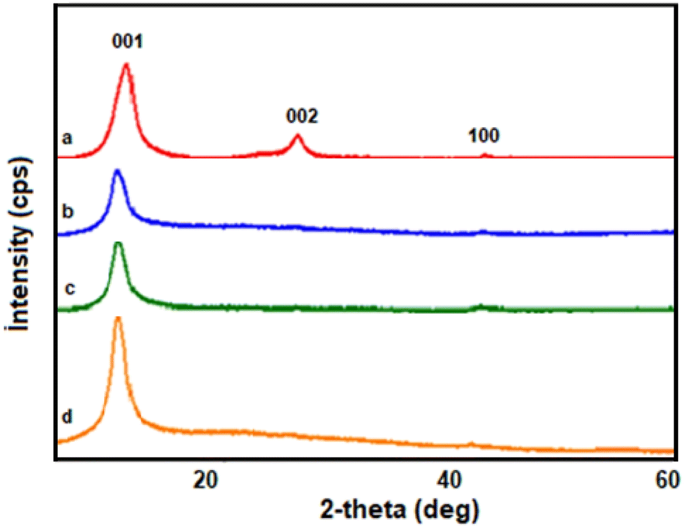 | ||
| Fig. 1 Diffractograms of GO exposed to different doses of gamma radiation: (a) non-irradiation; (b) 10 kGy; (c) 500 kGy; (d) 1500 kGy. | ||
From Fig. 1, the peak corresponding to GO exhibited a shift from 2θ = 11.98° to 2θ = 11.01° upon exposure to 10 kGy γ radiation. This shift can be attributed to an increase in the interlayer distance caused by the γ radiation. According to Bragg's law,22 a decrease in the diffraction angle indicates an increase in the interplanar spacing (d) when subjected to γ radiation.13 Under the influence of gamma rays, this type of shift may result in the production of vacancies in the crystal lattice, the formation of a defect structure, and the formation of residual stress. Particular irregularities in the crystal arrangement may develop as a result of their effect, as evidenced by shifts in the XRD spectrum. The crystallite sizes of non-irradiated GO, GO irradiated at 10 kGy, 500 kGy, and 1500 kGy were determined as d = 4.68 nm, d = 5.68 nm, d = 5.34 nm, and d = 2.34 nm, respectively. Furthermore, the peak corresponding to graphite completely disappeared, which can be attributed to the suppression of van der Waals interactions, an increase in the interlayer distance, and structural disruption caused by the radiation. During irradiation, the separated graphite layers undergo oxidation, resulting in the formation of larger GO particles. This phenomenon is evident in the XRD results, which display a decrease in the half-width of the peak from 1.78° to 1.47°. In Fig. 1c and d, it is apparent that the peaks have shifted to higher angles (2θ = 11.14° and 2θ = 11.27°) compared to Fig. 1b. This shift is attributed to the wrinkling and folding of the GO sheets at higher radiation doses, leading to an increased angle.
In this study, the structural properties of GO/PVA composite films containing 1 wt% and 5 wt% GO were examined before and after exposure to gamma radiation in Fig. 2. The XRD results of the GO/PVA composite film with non-irradiated 1 wt% and 5 wt% GO are presented in Fig. 2A-a and B-a, respectively. The main peak at 2θ = 19.90° corresponds to PVA,23 while additional peaks at 2θ = 14.11° and 2θ = 16.89° are observed in the non-irradiated sample. The absence of the characteristic GO peak in this pattern indicates the complete dispersion of GO into individual layers within the polymer matrix.24 The presence of the peaks at 2θ = 14.11° and 2θ = 16.89° suggests the formation of new oriented structures due to the incorporation of GO into the polymer.25
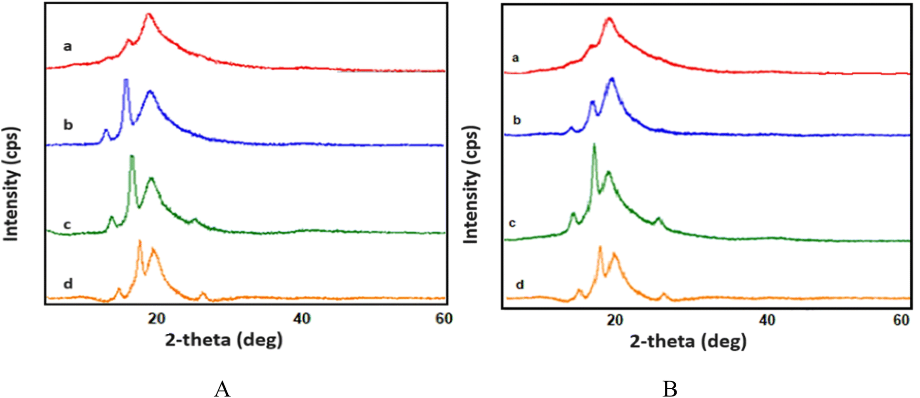 | ||
| Fig. 2 Diffractograms of GO/PVA composites with (A) 1 wt% and (B) 5 wt% concentration of GO exposed to different doses of gamma radiation: (a) non-irradiation; (b) 10 kGy; (c) 500 kGy; (d) 1500 kGy. | ||
Fig. 2 shows the structural properties of the 1 wt% GO/PVA composite film. Fig. 2A-b–d show the structural properties of samples irradiated with 10 kGy, 500 kGy, and 1500 kGy, respectively. As can be seen, the intensity of the peaks at 2θ = 14.11° and 16.89° increases under the influence of radiation. Starting at 500 kGy, an additional peak appears at 2θ = 25.40°. These peaks are thought to be due to gamma radiation breaking hydrogen bonds, tearing and wrinkling GO sheets, and creating new orientations. Also, Fig. 2B-b–d show that the intensity of additional peaks in the GO/PVA composite film increases due to γ radiation. This phenomenon can be attributed to breaking hydrogen bonds and separating GO particles, which enables the polymer to fill the spaces between these layers and form a new oriented structure.26 In the pattern of irradiated samples with doses of 500 kGy and 1500 kGy, a new peak at 2θ = 25.40° is observed. We believe that this peak emerges because of the wrinkling, folding, and stacking of the GO sheets, which becomes more pronounced at higher doses. At higher doses, hydrogen bonds are disrupted, the polymer undergoes softening, and the GO sheets fold, facilitating the penetration of the polymer between the layers and promoting the formation of a new oriented structure.
3.2 SEM and EDS results
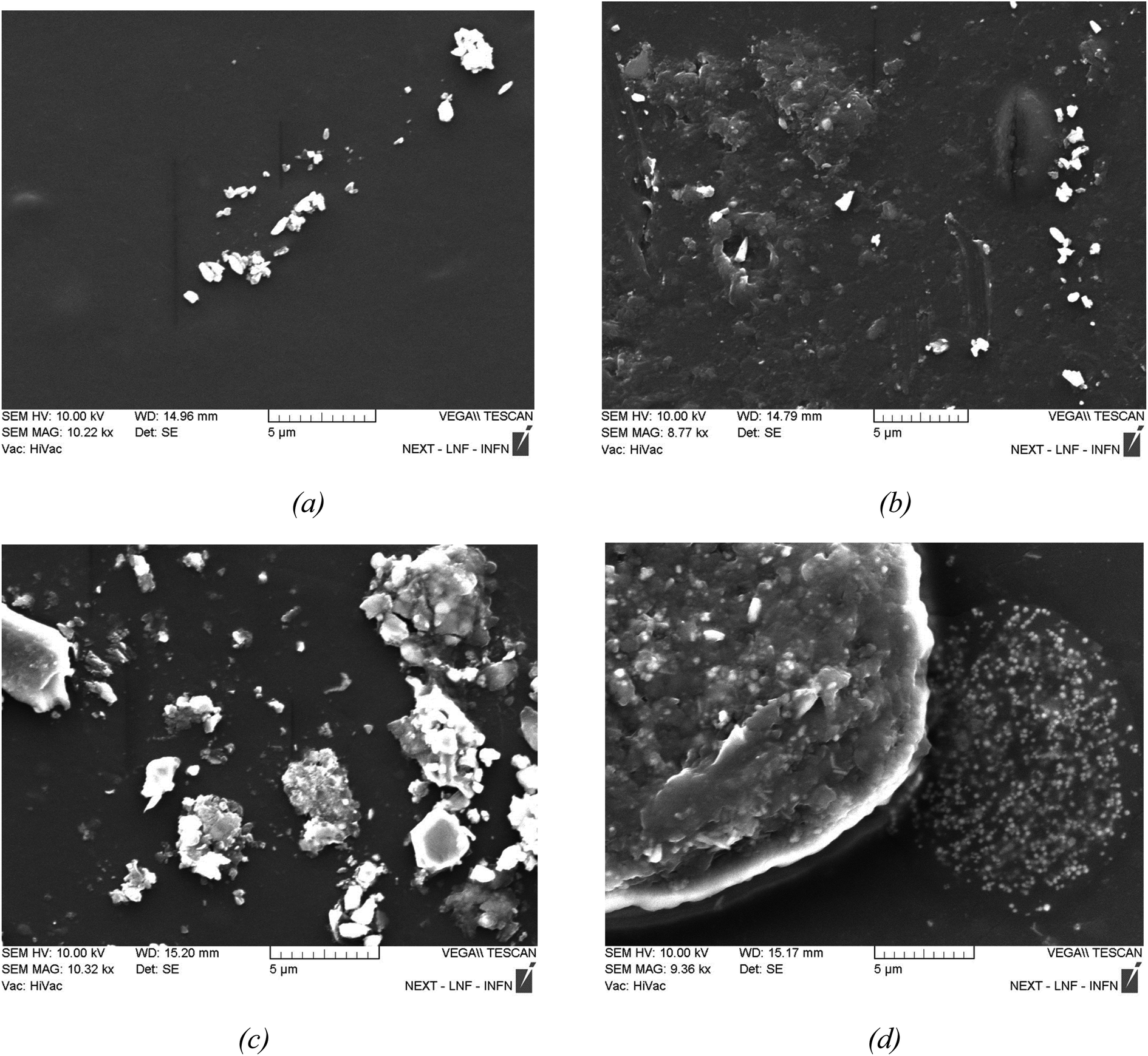
SEM can provide information on the morphology of a sample's surface. To obtain varied atomic percentages percent of GO on the PVA polymer matrix, the examined samples were irradiated with varying doses of gamma rays. In terms of investigating the surface of irradiated materials, morphology is thought to be particularly intriguing. SEM images of pure GO, 1 wt% GO/PVA, and 5 wt% GO/PVA are demonstrated in Fig. 3–5. | ||
| Fig. 3 SEM images of GO (a) non-irradiated; (b) 10 kGy; (c) 500 kGy; (d) 1500 kGy. | ||
 | ||
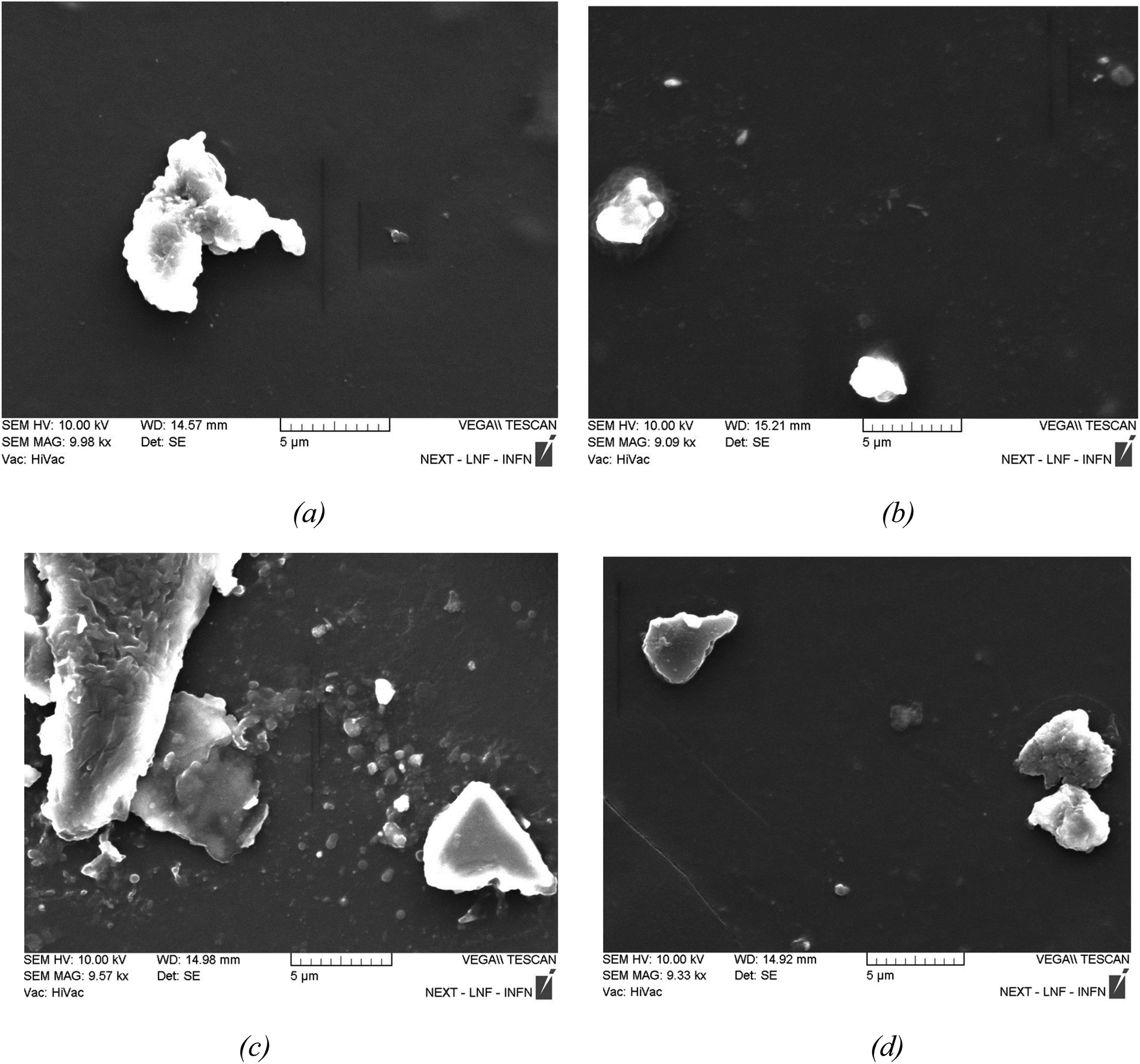
| Fig. 4 SEM images of 1 wt% GO/PVA (a) non-irradiated; (b) 10 kGy; (c) 500 kGy; (d) 1500 kGy. | ||
 | ||
| Fig. 5 SEM images of 5 wt% GO/PVA (a) non-irradiated; (b) 10 kGy; (c) 500 kGy; (d) 1500 kGy. | ||
Fig. 3a shows SEM images of pure and non-irradiated GO layers, while Fig. 3b shows pure GO layers irradiated with 10 kGy, 500 kGy, and 1500 kGy radiation doses. The thin monolayer GO layers are bound together to create multilayer GO, as shown in the SEM images of pure non-irradiated GO layers in Fig. 3a. Based on the cross-sectional area of GO in the photograph, we can see that a layer of adequate thickness has developed. Fig. 3b shows that relatively small particles are distributed on the surface of the layers formed after irradiation with a radiation dose of 10 kGy. As a result, these layers are broken into small pieces and smaller particles, disrupting the overall structure of the GO layer. This low-dose radiation disrupts the weak bonding contacts (van der Waals) between the layers of the GO layer, resulting in the creation of defects in the GO layer's surface structure. This is because the heating action of gamma radiation locally injected into pure GO layers disrupts the interlayer and van Der Waals forces between the layers, resulting in the production of smaller particles.
Fig. 3c depicts the delamination process in the layers as the dose of gamma rays increases. As the dose is increased, the ordered structure of the layers is disrupted, and tearing processes occur in the layers. In Fig. 3d, agglomeration formation is caused by van Der Waals and electrostatic interactions under the influence of a high dose. When we observe other images, the free-form group of the layers is disturbed (the process of agglomeration at the ends of the layers). Although certain GO layers are free, the space between them shrinks due to high-dose gamma radiation, and these layers bond together. As a result, the layers are assembled and form large-scale agglomerates.
Fig. 4a show a 1 wt% GO/PVA that has not been irradiated, Fig. 4b shows a 1 wt% GO/PVA that has been irradiated with a 10 kGy radiation dose, Fig. 4c shows a 1 wt% GO/PVA that has been irradiated with a 500 kGy radiation dose, and Fig. 4d shows a 1500 kGy radiation exposure. SEM images of a 1 wt% GO/PVA nanocomposite material are shown. The SEM picture of unirradiated 1 wt% GO/PVA shows that the GO is crystalline and randomly distributed on the surface of the PVA. It is assumed that GO was formed in the pores of PVA, while larger particles were distributed on the surface of the PVA polymer matrix.
Fig. 4b clearly illustrates the GO nanostructures generated in the lower layers (pores) as a result of the PVA matrix surface being destroyed by 10 kGy radiation. Fig. 4c depicts how the influence of 500 kGy radiation causes the GO nanostructures in the pores to agglomerate and form sharper crystalline formations. The image clearly shows that large and small agglomerates of varying sizes have formed here. The morphology of the sample obtained from the irradiation of 1 wt% GO/PVA nanocomposite film at a radiation dose of 1500 kGy shows that they form a mixed structure in a relatively dispersed form due to the high dose of radiation melting or breaking down the polymer and GO nanostructures. The strong radiation dose not only caused the PVA to melt due to the thermal effect, but it also shattered the GO nanostructures generated in the crystal structure into relatively smaller particles.
Fig. 5a depicts unirradiated 5% GO/PVA, Fig. 5b depicts 5% GO/PVA irradiated with 10 kGy dose, Fig. 5c depicts 5% GO/PVA irradiated with 500 kGy dosage, and Fig. 5d depicts 5% GO/PVA irradiated with 1500 kGy radiation dose. We present SEM photos of wt% GO/PVA nanostructures. The size of the non-irradiated 5 wt% GO/PVA (Fig. 5a) is greater than the size of the non-irradiated 1 wt% GO/PVA (Fig. 4a) based on the SEM pictures. This suggests that the mechanism of GO synthesis on the surface of the PVA matrix is the same and that increasing the proportion of GO leads to the formation of bigger nanostructures on the surface of the PVA polymer matrix. That is, GO layers are already created on the surface of PVA after the production process of GO in its pores (adsorption centers) finishes (saturation limit). As the atomic phase amount of GO increases, the process of manufacturing larger-size crystallites happens. When 5 wt% GO/PVA nanostructures are exposed to 10 kGy irradiation, the big agglomerates break down due to heat action, and smaller crystallites develop (see Fig. 5b). At a radiation dose of 500 kGy, tiny particles can be seen in addition to the large-sized aggregated GO layers in Fig. 5c. Other thick layers and agglomerates seen in Fig. 5c are fully shattered and smaller particles emerge at higher irradiation values (1500 kGy). As a result of the high-dose gamma radiation effect, the integrity of GO is destroyed, faults arise in the structure, and fragmentation ensues. Low dosages (10, 500 kGy) do not give enough energy to break the chemical connections between the layers, resulting in incomplete fragmentation. However, 1500 kGy of radiation is sufficient to disrupt these chemical bonds.
Fig. 6 illustrates the EDS results of 5 wt% GO/PVA composite film, both before and after exposure to irradiation at doses of 10 and 1500 kGy. In the non-irradiated sample, the EDS results show that the atomic percentages of carbon and oxygen are 65.48% and 34.52%, respectively. Fig. 6b displays the EDS outcomes of the 5 wt% GO/PVA composite film after being subjected to γ-irradiation at a dose of 10 kGy. Due to the radiation influence, the atomic percentage of oxygen decreased slightly from 34.52% to 34.48%. The sample irradiated at 1500 kGy exhibited the lowest atomic percentage of oxygen, measuring 32.75%. The C/O percentage ratio values for the non-irradiated, 10 kGy irradiated, and 1500 kGy irradiated samples are 1.897, 1.900, and 2.053, respectively. The increase in the C/O ratio indicates that the GO was reduced under the influence of γ radiation, resulting in the potential removal and decomposition of oxygen-containing functional groups into CO, CO2, and H2O.27 Furthermore, no peaks for other elements were detected in the EDS images, suggesting that the studied samples are chemically pure, based on these EDS results.
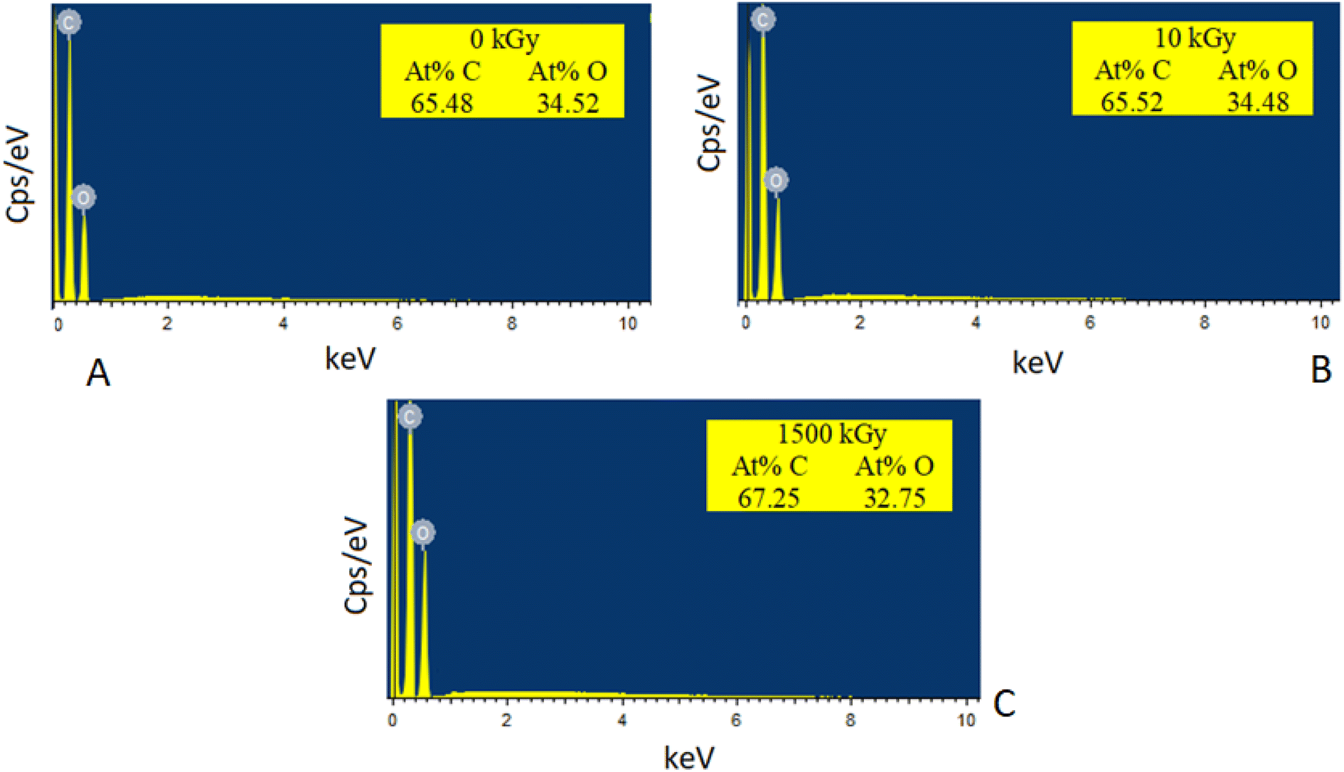 | ||
| Fig. 6 EDS results of γ-irradiated 5 wt% GO/PVA composites: (A) 0 kGy, (B) 10 kGy irradiated, (C) 1500 kGy irradiated samples. | ||
3.3 UV-Vis spectroscopy
The transmittance spectrum of 1 wt% and 5 wt% GO/PVA nanocomposite film material was investigated by an Ultraviolet-Visible (UV-Vis) spectrophotometer and shown in Fig. 7 for all samples.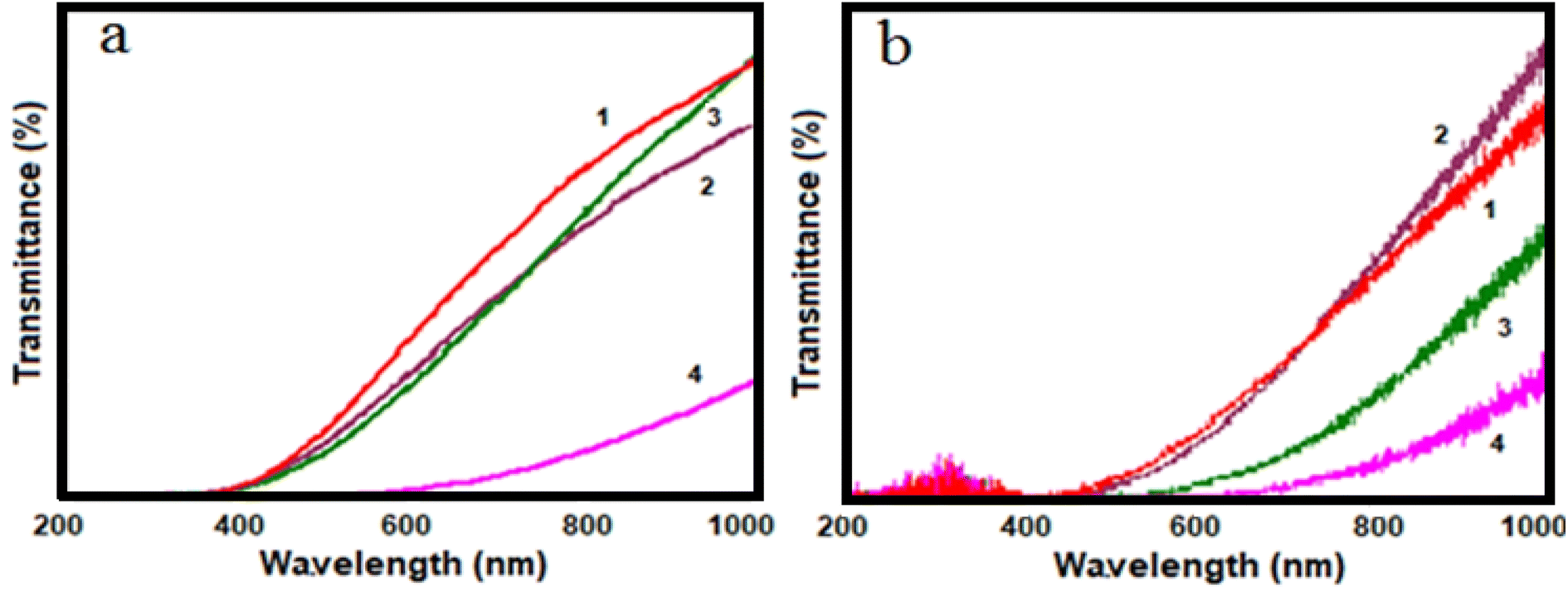 | ||
| Fig. 7 The transmittance spectrums of GO/PVA composite thin films with (a) 1 wt% and (b) 5 wt% concentration of GO, respectively: (1) 0 kGy; (2) 10 kGy; (3) 500 kGy; (4) 1500 kGy γ irradiated samples. | ||
Fig. 7a and b demonstrate a noticeable alteration in the transmittance spectrum of the samples following gamma radiation exposure. The lowest transmittance spectrum value is observed at the highest radiation dose (1500 Gy) due to the reduction of GO induced by gamma radiation. This reduction leads to an increase in absorption. However, the decrease in optical transmittance is not directly proportional to the dose value, as structural changes during radiation do not exhibit a linear dependence on gamma doses. Under the influence of gamma radiation, the breaking of hydrogen and hydroxyl groups has occurred in the PVA polymer, while the GO/PVA composite films undergo the disruption of hydrogen bonds.28,29 Because of these structural modifications, absorption increases, resulting in a decrease in the transmittance spectrum. The UV-Vis spectroscopy findings enable the observation of changes in the band gap value of both gamma-irradiated and non-irradiated samples about the radiation dose. The Tauc method was employed to determine the band gap value.30,31
The band gap values for PVA and GO are reported as 6.27 eV (ref. 32) and 2.20 eV,33 respectively. It should be noted that the band gap value of the reduced GO (rGO) can range from 1.00 eV to 1.69 eV depending on the degree of reduction. To determine the band gap energy of the samples, the linear portion of the curves was used to extrapolate to zero absorption (α = 0). The findings reveal that the band gap value decreases as the weight concentration of GO in the polymer increases. This can be attributed to the diminished distance between GO particles. Specifically, the band gap values for non-irradiated GO/PVA composites containing 1 wt% and 5 wt% GO are 2.69 eV and 1.88 eV, respectively. The alterations in band gap values of samples exposed to different doses of gamma radiation are presented in Table 1.
| Samples | Dose of gamma radiation (kGy) | |||
|---|---|---|---|---|
| Band gap value (eV) | ||||
| 0 | 10 | 500 | 1500 | |
| GO powder | 2.00 ± 0.02 eV | 1.60 ± 0.02 eV | 1.44 ± 0.02 eV | 1.33 ± 0.02 eV |
| 1% GO/PVA | 2.69 ± 0.02 eV | 2.60 ± 0.02 eV | 2.57 ± 0.02 eV | 2.00 ± 0.02 eV |
| 5% GO/PVA | 1.88 ± 0.02 eV | 1.63 ± 0.02 eV | 1.44 ± 0.02 eV | 1.20 ± 0.02 eV |
The addition of GO to PVA introduces new energy levels between the conduction and valence bands, leading to a decrease in the band gap value of the nanocomposite.28 This decrease becomes more prominent with an increased concentration of GO. As observed in the table, the band gap value decreases with higher doses of gamma radiation. This can be attributed to the presence of free radicals generated by the radiation, as well as the formation of new chemical bonds and localized states within the energy bands. The reduction of GO also occurs under the influence of gamma radiation.11 However, it is important to note that the band gap value is influenced by factors apart from the radiation dose, including particle size, interactions with the environment, and other factors.34 GO/PVA nanocomposites with adjustable optical properties hold significant potential for applications in polymer-based optoelectronic devices.35
The band gap value falls as the atomic percentage of GO in the PVA polymer matrix increases. Thus, although the Eg of a 1 wt% GO/PVA nanocomposite film is 2.69 eV, the Eg of a 5 wt% GO/PVA nanocomposite is 1.88 eV. The explanation for this is due to an increase in charge carrier density inside the PVA polymer matrix. As a result of the decrease in energy required for electronic transitions as charge carrier density increases, the value of Eg drops.
The Eg value decreased with increasing gamma radiation dosage in both cases (1 wt% and 5 wt%) GO/PVA nanocomposite. This drop is related to the creation of defect structures in the structure due to the action of gamma rays, which grow with increasing exposure, making the electron transition simpler. As a result, increasing the radiation exposure causes a drop in the Eg value.
3.4 FTIR spectroscopy
The samples were subjected to FTIR to assess the interaction between the elements in the GO/PVA nanocomposite film based on the percentage and dose of gamma radiation, and the findings are displayed in Fig. 8.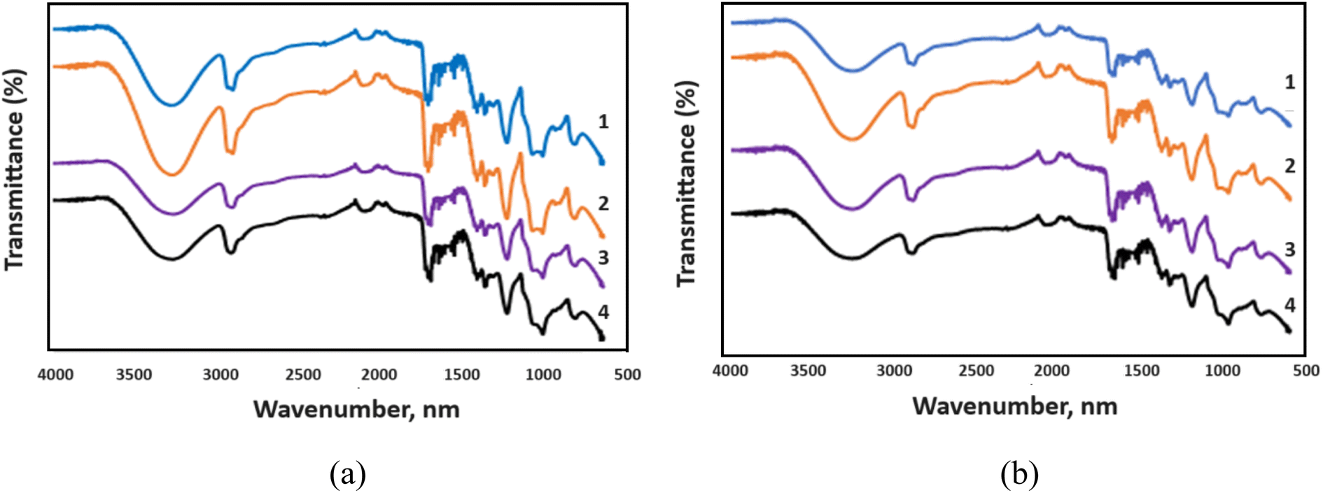 | ||
| Fig. 8 FTIR spectrum of (a) 1 wt% GO/PVA; (b) 5 wt% GO/PVA. (1) Non-irradiated; (2) 10 kGy; (3) 500 kGy; (4) 1500 kGy. | ||
FTIR spectroscopy, a valuable technique for analyzing graphene oxide, was employed to identify diverse functional groups, notably oxygen-based ones, present on the material. The FTIR results, depicted in Fig. 8, detail the impact of radiation doses (0, 10, 500, and 1500 kGy) on GO/PVA composite films. In the FTIR spectra of 1 wt% GO/PVA composite films, the broad peak at 3295–3307 cm−1 corresponds to the O–H stretching vibration of hydroxyl groups. Notably, its intensity varies with radiation, indicating the separation of oxygenated groups during exposure. Additionally, asymmetric and symmetric C–H stretching occurs at 2939 cm−1 and 2907 cm−1, respectively, in the spectrum of non-irradiated 1 wt% GO/PVA. In this spectrum, the peak at 1717 cm−1 signifies CO stretching of carboxyl groups.36,37 The films also exhibit CH/CH2 deformation vibrations around 1323 cm−1.38 The band at 1083 cm−1 is assigned to the C–O stretching vibrations of C–O–C. The peak at 944 cm−1 corresponds to the epoxy or peroxide group.39–41 This characteristic peak shifts to a wavelength of 970 cm−1 in the spectrum of 1500 kGy irradiated 1 wt% GO/PVA composite. This is due to the separation of oxide groups due to the reduction process caused by radiation. The bands observed in the spectrum of 1 wt% GO/PVA composite are very similar to the bands that appeared in the spectrum of 5 wt% GO/PVA composite.
3.5 Raman microscopy
The Raman spectra of samples are reflected in Fig. 9. The G peak, characteristic of all carbon structures corresponding to the C–C stretching within the range of 1584–1607 cm−1, is observed for all samples. At low and medium radiation doses, the strength of the characteristic peak corresponding to the G band is relatively reduced, which is related to the vibration of sp2 hybridization bonds and relative structure degradation. Nevertheless, the outcomes documented in the academic literature reveal that the peaks identified in the case of pure PVA are not conspicuously observed.42 The intensity of the G band will increase further compared to the initial sample at the highest dose of radiation (1500 kGy), resulting in the formation of graphene or its derivatives, the re-establishment of connections between carbon atoms, and the development of a new structure due to the reconstruction processes between GO layers.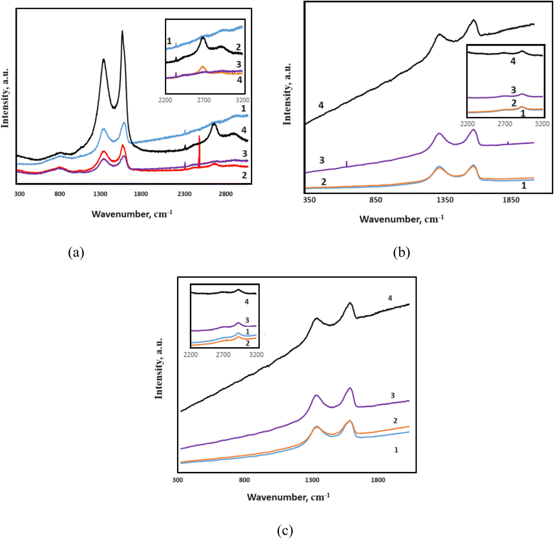 | ||
| Fig. 9 Raman spectrum of irradiated at different doses of (a) GO; (b) 1 wt% GO/PVA; (c) 5 wt% GO/PVA. | ||
Additionally, the D peak at 1358–1366 cm−1 is noticed, indicating distortions in the sample's structure.43,44 As previously stated, the strength of the G band increased with increasing radiation dose. A decrease in defects is shown by an increase in the intensity of the D band at the highest radiation dose, according to the same criteria. This demonstrates that GO layer reassembly happens at the maximum radiation dose, implying that defect structures are eliminated. The ID/IG ratios were measured dependent on radiation dozes. For irradiated samples at 0, 10, 500, and 1500 kGy, the ID/IG ratios are recorded as 0.90, 0.83, 0.93, and 0.82 respectively, and given in Table 2. The tendency of these values to change is associated with the removal of oxide groups, bends in the sheets, etc., depending on the dose. Calculations show that at a dose of 500 kGy, more defects and distortions are observed. Notably, in samples irradiated at doses of 10 and 1500 kGy (Fig. 9b and c), the 2D peak is observed. This is related to the tendency of GO sheets to stack on top of each other. At 1500 kGy, the intensity of this peak sharply increases, indicating sharper stacking of the sheets. Additionally, at 1500 kGy, the G + D peak is also visible, which is associated with defects and twisting of the sheets due to radiation effects.45
| Samples | ID/IG | |||
|---|---|---|---|---|
| Non-radiation | 10 kGy | 500 kGy | 1500 kGy | |
| GO | 0.90 | 0.83 | 0.93 | 0.82 |
| 1 wt% GO/PVA | 0.95 | 0.94 | 0.96 | 0.92 |
| 5 wt% GO/PVA | 0.92 | 0.88 | 0.93 | 0.91 |
Raman spectra for 1 wt% and 5 wt% GO/PVA composite films are depicted in Fig. 7b and c. The D peak at 1355 cm−1 and the G peak at 1609 cm−1 are observed for the samples. Moreover, a small peak at 2908 cm−1, characteristic of PVA and corresponding to the –CH2 vibration, is also noted.46 It is evident that the highest value of the ratio is observed in the composite materials at 500 kGy, as shown in the Fig. 9.
4. Conclusion
This study involved the synthesis of GO using a modified Hummers' method, followed by the preparation of composites with PVA at different weight concentrations (1 wt% and 5 wt%). Initially, it was observed that incorporating PVA into GO resulted in a decrease in the band gap. This decrease in the band gap was attributed to the creation of new energy levels between the conduction and valence bands within the PVA/GO composite film. The investigation also explored the impact of gamma radiation at various doses on both GO and GO/PVA composites. The exposure to gamma radiation induced structural modifications in the GO/PVA composite film. The radiation caused the breakage of hydrogen bonds, separation of GO sheets, and the incorporation of polymer between the GO sheets, leading to the formation of new cross bonds. Consequently, the diffraction peaks exhibited new features due to changes in bond configurations and the creation of a distinct polymer structure surrounding the GO sheets. Gamma radiation was found to break or deform the bonds between the polymer and GO, resulting in the formation of radicals. These radicals contributed to the decrease in the band gap by generating intermediate energy levels. Additionally, gamma radiation caused the reduction of GO, which was confirmed by the EDS results, providing evidence for the reduction of graphene oxide. Comparing the two composites, it was observed that the band gap value decreased with an increase in the concentration of GO. Therefore, by adjusting either the concentration of GO within the composite or the radiation exposure, control over the band gap value of the sample could be achieved. However, it was noted that both the structural and optical properties did not exhibit a linear dependence on the radiation dose. Furthermore, the XRD results indicated the disintegration and oxidation of the residual graphite structure under the influence of gamma radiation, as well as its combination with GO. FT-IR and Raman spectroscopy confirm the formation of GO. According to Raman spectroscopy results, the ID/IG ratios were calculated as 0.90, 0.83, 0.93, and 0.82 for 0, 10, 500, and 1500 kGy irradiated GO, respectively, and changes in these values is ascribed to the removal of oxide groups, bends in the sheets depending on the dose. The SEM images demonstrated that when the radiation dose increases, the breakdown of GO on the polymer's surface occurs, and at the highest dose, radiation heating causes the distribution of GO and PVA in the pores.Conflicts of interest
There are no conflicts to declare.References
- T. N. Ghosh, S. S. Pradhan, S. K. Sarkar and A. K. Bhunia, J. Mater. Sci.: Mater. Electron., 2021, 32(14), 19157–19178 CrossRef CAS.
- F. Pendolino and N. Armata, Graphene Oxide in Environmental Remediation Process, SpringerBriefs in Applied Sciences and Technology, Springer Cham, 1st edn, 2017 Search PubMed.
- A. Dimiev, D. V. Kosynkin, L. B. Alemany, P. Chaguine and J. M. Tour, J. Am. Chem. Soc., 2012, 134(5), 2815–2822 CrossRef CAS PubMed.
- R. T. M. Ahmad, S. H. Hong, T. Z. Shen and J. K. Song, Carbon, 2016, 98, 188–194 CrossRef CAS.
- H. Wadhwa, G. Kandhol, U. P. Deshpande, S. Mahendia and S. Kumar, Colloid Polym. Sci., 2020, 298(10), 1319–1333 CrossRef CAS.
- A. M. Akbas, A. Tataroğlu, S. Altındal and Y. Azizian-Kalandaragh, J. Mater. Sci.: Mater. Electron., 2021, 32(6), 7657–7670 CrossRef CAS.
- X. Wu, Y. Xie, C. Xue, K. Chen, X. Yang and L. Xu, et al., Mater. Res. Express, 2019, 6(7), 075306 CrossRef CAS.
- L. Gahramanli, M. Muradov, G. Eyvazova, M. Baghirov, S. Mammadyarova, G. Aliyeva, E. Hajiyev, F. Mammadov and S. Bellucci, Chem. Eng., 2023, 7(5), 92 CAS.
- K. M. Abu Hurayra-Lizu, M. W. Bari, F. Gulshan and M. R. Islam, Heliyon, 2021, 7(5), e06983 CrossRef CAS PubMed.
- B. W. Chieng, N. A. Ibrahim, N. A. Daud and Z. A. Talib, Functionalization of Graphene Oxide via Gamma-Ray Irradiation for Hydrophobic Materials, in Synthesis, Technology and Applications of Carbon Nanomaterials, Micro and Nano Technologies, ed. S. A. Rashid, R. N. Othman and M. Z. Hussein, Elsevier, 2019,, ch. 8, pp. 177–203 Search PubMed.
- T. A. Jassim and A. A. Saeed, IOP Conf. Ser.: Mater. Sci. Eng., 2020, 928(7), 072137 CAS.
- M. M. Atta, M. E. Habieb, M. Abd El Hameed Mohamed, D. M. Lotfy and E. O. Taha, New J. Chem., 2022, 46, 4406–4420 RSC.
- M. Muradov, M. B. Baghirov, G. Eyvazova, L. Gahramanli, S. Mammadyarova, G. Aliyeva and M. Abdullayev, Radiat. Phys. Chem., 2023, 208, 110926 CrossRef CAS.
- J. Guerrero-Contreras and F. Caballero-Briones, Mater. Chem. Phys., 2015, 153, 209–220 CrossRef CAS.
- E. Sujiono, H. Zurnansyah, D. Zabrian, M. Y. Dahlan, B. D. Amin and J. Samnur Agus, Heliyon, 2020, 6(8), 04568 CrossRef PubMed.
- M. J. Yoo and H. B. Park, Carbon, 2019, 141, 515–522 CrossRef CAS.
- D. Bhatnagar, S. Singh, S. Yadav, A. Kumar and I. Kaur, Mater. Res. Express, 2019, 4(1), 015101 CrossRef.
- Y. Shi, D. Xiong, J. Li, K. Wang and N. Wang, RSC Adv., 2017, 7(2), 1045–1105 RSC.
- Q. T. Ain, S. H. Haq, A. Alshammari, M. A. Al-Mutlaq and M. N. Anjum, Beilstein J. Nanotechnol., 2019, 10(1), 901–911 CrossRef CAS PubMed.
- R. Siburian, H. Sihotang, S. L. Raja, M. Supeno and C. Simanjuntak, Orient. J. Chem., 2018, 34(1), 182 CrossRef CAS.
- A. T. Nguyen, Y. Lee, P. Q. H. Nguyen, P. Dera, S. H. Yoon and W. Lee, Sci. Rep., 2022, 12(1), 1–7 CrossRef PubMed.
- M. Dudley and X. R. Huang, Encyclopedia of Materials: Science and Technology, 2001, pp. 9813–9825 Search PubMed.
- X. Hong, L. Zou, J. Zhao, C. Li and L. Cong, IOP Conf. Ser.: Mater. Sci. Eng., 2018, 439, 042011 CrossRef.
- M. Aslam, M. A. Kalyar and Z. A. Raza, J. Mater. Sci.: Mater. Electron., 2017, 28(18), 13401–13413 CrossRef CAS.
- J. Ma, Y. Li, X. Yin, Y. Xu, J. Yue, J. Bao and T. Zhou, RSC Adv., 2016, 6(55), 49448–49458 RSC.
- W. H. Eisa, Y. K. Abdel-Moneam, Y. Shaaban, A. A. Abdel-Fattah and A. M. Abou Zeid, Mater. Chem. Phys., 2011, 128(1–2), 109–113 CrossRef CAS.
- I. Sánchez-García, A. Nunez, L. J. Bonales, J. M. Perlado and J. Cobos, Radiat. Phys. Chem., 2019, 165, 108395 CrossRef.
- P. Tiamduangtawan and K. Saenboonruang, J. Phys.: Conf. Ser., 2019, 1285 Search PubMed.
- N. M. El-Sawy, M. B. El-Arnaouty and A. A. Ghaffar, Polym.-Plast. Technol. Eng., 2010, 49(2), 169–177 CrossRef CAS.
- O. G. Abdullah, S. B. Aziz, K. M. Omer and Y. M. Salih, J. Mater. Sci.: Mater. Electron., 2015, 26(7), 5303–5309 CrossRef CAS.
- L. Haryński, A. Olejnik, K. Grochowska and K. Siuzdak, Opt. Mater., 2022, 127, 112205 CrossRef.
- O. G. Abdullah, S. B. Aziz and M. A. Rasheed, Results Phys., 2016, 6, 1103–1108 CrossRef.
- P. Sehrawat, S. S. Islam, P. Mishra and S. Ahmad, Sci. Rep., 2018, 8(1), 1–13 Search PubMed.
- L. Gahramanli, M. Muradov, Y. Azizian, G. Eyvazova and O. Balayeva, Int. J. Mod. Phys. B, 2023, 2350103 CrossRef CAS.
- M. Aslam, M. A. Kalyar and Z. A. Raza, Appl. Phys. A: Mater. Sci. Process., 2017, 123(6) Search PubMed.
- A. Mustafa, N. Yaqoob, M. Almas, S. Kamal, K. M. Zia and S. Rehman, J. Polym. Res., 2022, 29(8), 332 CrossRef CAS.
- T. F. Emiru and D. W. Ayele, Egyptian Journal of Basic and Applied Sciences, 2017, 4(1), 74–79 CrossRef.
- T. Wang, Y. Li, S. Geng, C. Zhou, X. Jia, F. Yang, L. Zhang, X. Ren and H. Yang, RSC Adv., 2015, 5(108), 88958–88964 RSC.
- D. He, Z. Peng, W. Gong, Y. Luo, P. Zhao and L. Kong, RSC Adv., 2015, 5(16), 11966–11972 RSC.
- T. K. Dey, M. Jamal and M. E. Uddin, Journal of Water Process Engineering, 2023, 52, 103554 CrossRef.
- R. P. Chahal, S. Mahendia, A. K. Tomar and S. Kumar, J. Alloys Compd., 2012, 538, 212–219 CrossRef CAS.
- R. P. Chahal, S. Mahendia, A. K. Tomar and S. Kumar, Opt. Mater., 2016, 52, 237–241 CrossRef CAS.
- V. Scardaci and G. C. Compagnini, MDPI, 2021, 7(2), 48, DOI:10.3390/c7020048.
- E. Bîru and H. Iovu, Raman Spectrosc., 2018, 9, 179 Search PubMed.
- Y. Yan, S. Manickam, E. Lester, T. Wu and C. H. Pan, Ultrason. Sonochem., 2021, 73, 105519 CrossRef CAS PubMed.
- Y. Kan, J. V. Bondareva, E. S. Statnik, J. Cvjetinovic, S. Lipovskikh, A. S. Abdurashitov, M. A. Kirsanova, G. B. Sukhorukhov, S. A. Evlashin, A. I. Salimon and A. M. Korsunsky, Nanomaterials, 2022, 12(6), 998 CrossRef CAS PubMed.
| This journal is © The Royal Society of Chemistry 2023 |