
 Open Access Article
 This Open Access Article is licensed under a Creative Commons Attribution-Non Commercial 3.0 Unported Licence
Synthesis of component-controllable monolayer MoxW(1−x)S2ySe2(1−y) alloys with continuously tunable band gap and carrier type†
You Liab,
Kangkang Wang b,
Yiwen Wanga,
Ziyue Qianb,
Wenbin Huanga,
Junqi Wanga,
Qichao Yanga,
Honggang Wangb,
Junyi Liaob,
Sabir Hussainb,
Liming Xieb and
Junjie Qi*a
b,
Yiwen Wanga,
Ziyue Qianb,
Wenbin Huanga,
Junqi Wanga,
Qichao Yanga,
Honggang Wangb,
Junyi Liaob,
Sabir Hussainb,
Liming Xieb and
Junjie Qi*a
aSchool of Materials Science and Engineering, University of Science and Technology Beijing, Beijing 100083, P. R. China. E-mail: junjieqi@ustb.edu.cn
bCAS Key Laboratory of Standardization and Measurement for Nanotechnology, National Center for Nanoscience and Technology, Beijing 100190, China
First published on 24th November 2023
Abstract
Alloying can effectively modify electronic and optical properties of two-dimensional (2D) transition metal dichalcogenides (TMDs). However, efficient and simple methods to synthesize atomically thin TMD alloys need to be further developed. In this study, we synthesized 25 monolayer MoxW(1−x)S2ySe2(1−y) alloys by using a new liquid phase edge epitaxy (LPEE) growth method with high controllability. This straightforward approach can be used to obtain monolayer materials and operates on a self-limiting growth mechanism. The process allows the liquid solution to come into contact with the two-dimensional grains only at their edges, resulting in epitaxy confined only along the in-plane direction, which produces exclusively monolayer epitaxy. By controlling the weight ratio of MoS2/WSe2 (MoSe2/WS2), 25 monolayer MoxW(1−x)S2ySe2(1−y) alloys with different atomic ratios can be obtained on sapphire substrates, with band gap ranging from WS2 (1.55 eV) to MoSe2 (1.99 eV) and a continuously broad spectrum ranging from 623 nm to 800 nm. By adjusting the alloy composition, the carrier type and carrier mobility of alloy-based field-effect transistors can be modulated. In particular, the adjustable conductivity of MoxW(1−x)S2ySe2(1−y) alloys from n-type to bipolar type is achieved for the first time. This general synthetic strategy provides a foundation for the development of monolayer TMD alloys with multiple components and various 2D materials.
1. Introduction
Unlike zero-bandgap graphene, monolayer transition metal dichalcogenides (TMDs) have a tunable direct bandgap and can be used to fabricate semiconductor devices with excellent performance.1–10 However, acquiring continuous bandgap tuning is difficult for monolayer TMDs, likely because of certain disadvantages, such as relatively limited variety and uniformity. These drawbacks limit the ability of TMDs to meet diverse electronic and optoelectronic application requirements. Therefore, various strategies have been developed to optimize the energy band structure of TMDs. These methods include doping,11–14 heterostructure engineering,15–17 surface functionalization, and alloying.18–26 Meanwhile, the band gap of 2D TMDs can also be tuned by adjusting the number of layers,27 as well as by applying stresses and electric fields.28–32 Among these approaches, alloying is an easily scalable technique that can be used to design energy band structures.Ternary monolayer TMD alloys such as WS2xSe2(1−x), MoS2(1−x)Se2x, and ReS2xSe2(1−x) have exhibited versatile optical and electronic properties.33–36 By tuning the ratio of S to Se,23 the direct band gap of the monolayer MoS2(1−x)Se2x alloy can be tuned completely from pure MoSe2 (x = 1, Eg = 1.56 eV) to pure MoS2 (x = 0, Eg = 1.86 eV). Alloying also allows for the structural and phase transformation of monolayer TMDs (e.g., rapid phase control from 1H to DT in single-molecule layer W1−xRexS2 alloys by adjusting the ratio of Re/W).26 In addition, monolayer TMD alloys have lower free and internal energies, resulting in improved thermal stability. Various synthesis techniques have been developed to obtain high-quality monolayer TMD alloys. Xie et al. prepared monolayer MoS2(1−x)Se2x materials with multiple components by physical vapor deposition (PVD).37 Xiang et al. fabricated high-quality monolayer WS2(1−x)Se2x materials with tunable forbidden bandgap widths by chemical vapor deposition (CVD) on SiO2/Si substrates.34 Using a sodium chloride-assisted confined-space CVD method, Xiao et al. synthesized large-size monolayer WeS2(1−x)Se2x films on SiO2/Si substrates.38 The aforementioned strategies show potential for growing high-quality TMD alloys, but these synthesis techniques are uncontrollable and complicated. For instance, the PVD method requires good stability and easy sublimation of the precursor at the growth temperature, so the growth temperature and precursor are critical parameters in the TMD alloys growth process, and unsuitability of either parameter can produce by-products. In conventional CVD, the precursor vapor pressure determines the growth directly. The vapor pressure in CVD is closely associated with the reaction temperature and the precursor-substrate distance, and minor variations in these two parameters may induce sharp vapor pressure fluctuations, leading to the generation of undesired by-products during the synthesis process of TMD alloys. Meanwhile, confined-space CVD method is complicated by the requirement of a suitable confinement strategy to be designed. Moreover, studies on the synthesis of TMD alloys have mostly focused on ternary TMD alloys and rarely on quaternary TMD alloys. The synthesis of high-quality tunable quaternary monolayer TMD alloys continues to present a significant challenge.
According to the liquid phase edge epitaxy (LPEE) growth mechanism previously proposed by our research group,39 25 monolayer MoxW(1−x)S2ySe2(1−y) alloys with different atomic ratios can be obtained on sapphire substrates. In LPEE, the solution only contacts the edges of the two-dimensional grains, restricting epitaxy in the in-plane direction. Consequently, monolayer alloys are formed. By adjusting the weight ratio of MoS2 and WSe2 (MoSe2 and WS2) powders, MoxW(1−x)S2ySe2(1−y) monolayer alloys with different atomic ratios can be obtained, and the bandgap of the as-grown alloys can be continuously adjusted from WS2 (1.55 eV) to MoSe2 (1.99 eV). Due to the adjustable bandgap, quaternary TMD alloys have a wide range of applications in the fields of switching devices, radio frequency (RF) devices, optoelectronic devices, and so on. This LPEE method is applicable for the preparation of high-quality and controllable quaternary monolayer TMD alloys with precise tunability of composition. The atomic ratio of each component in the MoxW(1−x)S2ySe2(1−y) alloys was calculated using X-ray photoelectron spectroscopy (XPS). Variations in the electronic bandgap of 25 quaternary TMD alloys with different component ratios were measured using photoluminescence (PL). The complex structural arrangement of monolayer MoxW(1−x)S2ySe2(1−y) was investigated using scanning transmission electron microscopy (STEM). By adjusting alloys composition, carrier type and carrier mobility of alloy-based field-effect transistors can be modulated. In particular, the adjustable conductivity of MoxW(1−x)S2ySe2(1−y) alloys from n-type to bipolar type is achieved.
2. Experimental
2.1. Material growth
Monolayer MoxW(1−x)S2ySe2(1−y) were obtained in a single-temperature zone CVD tube furnace (Fig. S1†). MoSe2 (MoS2) powder (99.99%, Macklin) and WS2 (WSe2) powder (99.99%, Macklin) in different mass ratios were mixed (total weight = 0.05 g) and then placed inside the quartz boat, together with 1 g of NaCl powder (99.5%, Macklin) as precursors. Sapphire wafers (∼10 × 18 mm2) as substrates were treated with a mixture consisting of acetone, ethanol, and isopropanol. They were then placed upside down on a quartz vessel at the center of the furnace. Prior to heating, the system was vacuum-pumped for 15 min and flushed with 500 sccm Ar (99.999% purity) gas to remove air. Pumping was subsequently discontinued to allow the pressure in the system to return to atmospheric pressure. The furnace temperature was raised to the growth temperature (900 °C) within 30 min and maintained for 1 h. During the growth, 10 sccm Ar gas was used as the carrier gas. After the heating was discontinued, the furnace temperature was allowed to decrease to 500 °C before the chamber door was opened. The chamber was allowed to rapidly cool down to room temperature. The alloys were removed from the chamber. The surfaces were gently washed with deionized water to remove the extra salt and then blown dry with nitrogen gas for preservation.2.2. Preparation and characterization of TEM/STEM samples
The monolayer as-grown samples were transferred onto Cu grids via a wet polymethyl methacrylate (PMMA) transfer method. A PMMA layer (3000 rpm for 60 s) was spin-coated on the substrate with deposited samples. This operation was performed thrice. Substrate was then baked at 120 °C for 20 min. The PMMA/MoxW(1−x)S2ySe2(1−y) film on the sapphire was then transferred onto a Cu grid by using tape. It was then soaked in acetone for 40 min at 60 °C until the PMMA was removed. Finally, the copper grid was washed with isopropanol and subsequently removed from it until it was dry.TEM and STEM images, selected area electron diffraction (SAED) mode, and energy-dispersive spectroscopy (EDS) maps were acquired on a JEM-F200 (JEOL) unit operating at 200 kV. The high-angle annular dark-field scanning transmission electron microscopy (HAADF-STEM) images were recorded using a transmission electron microscope with a double Cs-corrected JEM-ARM200CF (JEOL) operated at 80 kV, equipped with a CEOS Cs corrector (CEOS GmbH, Heidelberg, Germany).
2.3. Raman and photoluminescence spectroscopy
Raman/PL characterization was conducted using a Raman microscope (Renishaw inVia) with a laser wavelength of 532 nm, power of 10%, and PL power of 1%. Raman maps were set in steps of 0.5 μm. Image processing was performed using the software Renishaw Wire 4.2.2.4. DFT calculation
Density functional theory (DFT) simulation was conducted by Vienna Ab initio Simulation Package (VASP) software with the projector augmented wave (PAW) method. The convergence value of energy was set as 10−5 eV, and the convergence value of force on each atom was 0.05 eV Å−1. Hubbard-U correction was added.2.5. Characterization of morphology and composition
Optical images of monolayer MoxW(1−x)S2ySe2(1−y) alloys were captured by optical microscopy (OM, Olympus, BX51) and atomic force microscopy (AFM, Bruker, Dimension Icon). X-ray photoelectron spectroscopy (XPS) spectra were acquired using the ESCALAB 250Xi (ThermoFisher Scientific, UK) and 200 eV X-rays (Al K-alpha). XPS peaks were analyzed and fitted using the software Advantage and Original.2.6. Device fabrication and measurement
The mask was utilized to pattern the source and drain. Cr/Au electrodes were deposited with thickness of 10/60 nm by electron beam evaporation system. Electrical transport measurements of alloy FETs under vacuum were conducted by a Keithley 4200-SCS semiconductor analyzer.3. Result and discussion
As shown in Fig. 1a, the atomic scheme for the nucleation and growth procedure in LPEE comprises eutectic melting, nucleation and growth, and the remaining monolayer TMD alloys. In Stage 1, the molten salt (solvent) and TMD precursors (solute) melted above the eutectic melting point temperature. At elevated vapor pressure and temperature, partial evaporation of the molten salt led to the supersaturation of the solution. Consequently, the monolayer TMD alloys began to nucleate and crystallize (Stage 2). The growth of the alloy flakes was driven by the motion of the droplets, which only touched the edges of the alloy flakes. This limited contact physically prevented the nucleation and growth of alloy flakes and inhibited the growth of alloy flakes with few layers. Finally, most of the molten salt evaporated and the monolayer TMD alloys remained on the substrate (Stage 3).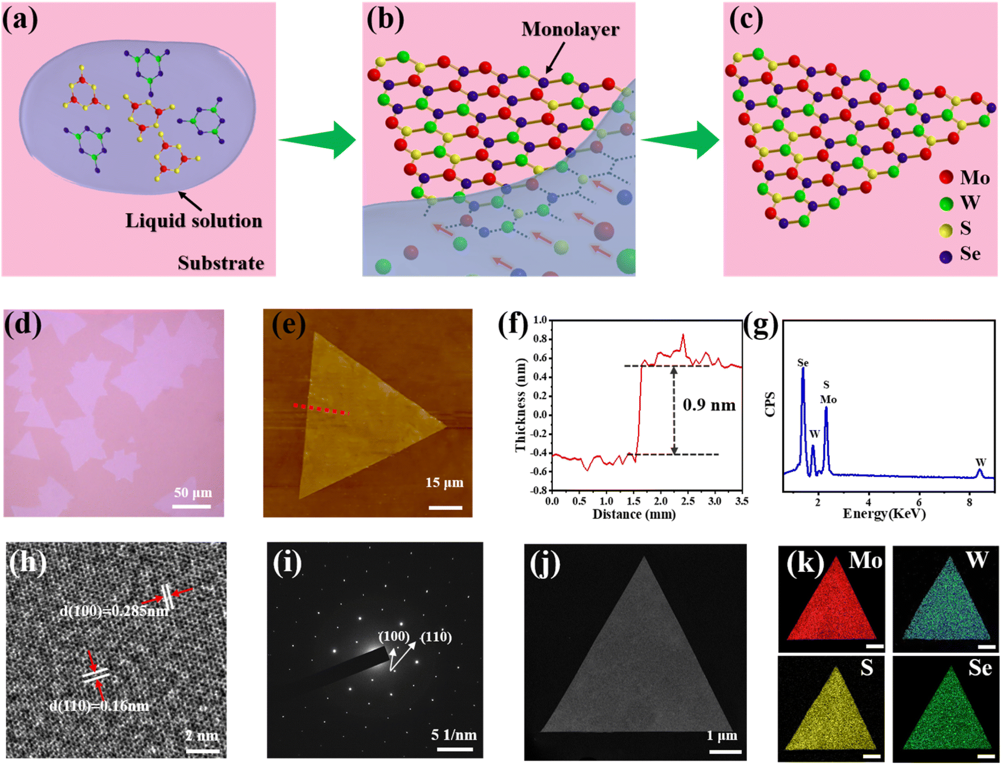 | ||
| Fig. 1 Synthesis of monolayer MoxW(1−x)S2ySe2(1−y) by LPEE. (a)–(c) Schematic of the nucleation and growth of MoxW(1−x)S2ySe2(1−y). (d) OM image of Mo0.82W0.18S0.28Se1.72 on the sapphire substrate. (e) AFM image of Mo0.82W0.18S0.28Se1.72. (f) Height profile (along the red dashed line) in the AFM images of Mo0.82W0.18S0.28Se1.72. (g) EDS elemental analysis of Mo0.82W0.18S0.28Se1.72. (h) HRTEM image of Mo0.82W0.18S0.28Se1.72. (i) SAED image of Mo0.82W0.18S0.28Se1.72. (j) STEM image of Mo0.82W0.18S0.28Se1.72 on Cu grids. (k) EDS mapping images of the elements Mo, W, S, and Se in Mo0.82W0.18S0.28Se1.72. Scale bar: 1 μm. | ||
As shown in Fig. 1d, the quaternary Mo0.82W0.18S0.28Se1.72 is successfully synthesized using LPEE. The synthesized Mo0.82W0.18S0.28Se1.72 alloy is monolayer with regular triangular morphologies, and other quaternary alloys with irregular shapes may be attributed to the competition of different boundary free energies, which determine the growth rate of each edge, ultimately affecting the morphological structure.8 The quaternary Mo0.82W0.18S0.28Se1.72 alloy was confirmed as monolayer structures by AFM. Fig. 1e and f presents the AFM images and height profiles of the isolated flakes, the heights of the flakes are about 0.9 nm, which is consistent with the height of a monolayer alloy.40–42 These flakes have a smooth flat surface with uniform thickness and no cracks.
To evaluate the crystallinity of the grown monolayer MoxW(1−x)S2ySe2(1−y) obtained using the proposed LPEE method, we selected the monolayer Mo0.82W0.18S0.28Se1.72 as representative for electron microscopy characterization. During the wet transfer process, we used PMMA as a transfer film to move the grown alloys from the sapphire substrate to the Cu grids for TEM characterization. As shown in Fig. 1h, the HRTEM image of the monolayer Mo0.82W0.18S0.28Se1.72 shows a honeycomb structure exhibiting a clear hexagonal atomic arrangement, with a spacing of about 0.16 nm in the (110) crystal plane direction and 0.285 nm in the (100) crystal plane. As shown in Fig. 1i, SAED shows 6 identical diffraction spots, indicating the single crystal nature and good crystallinity of the monolayer Mo0.82W0.18S0.28Se1.72.43–47 Fig. 1k presents the EDS mapping images, and the corresponding EDS spectra are shown in Fig. 1g, which reveals the uniform distribution of Mo, W, S, and Se in the alloy.
Raman spectroscopy was conducted to analyze the structural composition of the synthesized quaternary monolayer MoxW(1−x)S2ySe2(1−y). The Raman spectra of MoxW(1−x)S2ySe2(1−y) synthesized with different weight ratios of MoS2 and WSe2 powders reveal two different in-plane vibrational peaks in the spectrum (Fig. 2a), caused by the E2g1 vibrational modes of the Mo–S and W–S bonds, respectively.23,24 As the MoS2 content increased, the E2g1 mode peak of WS2 produces a blueshift, whereas the E2g1 mode peak of MoS2 produces a redshift. Three major peaks are also observed. The first peak at the low frequency can be attributed to the (E2g(S–W) − LA(S–W) + A1g(Se–W) − LA(Se–W)) W–S–Se bond vibration, with LA denoting the longitudinal acoustic mode.25 The second peak corresponds to the Mo–W–Se bond vibration. The third peak is the Mo–W–S bond vibration attributed to the combined A1g peak of Mo–S and W–S. We further observed that when x is 0.67 and y is 0.69, the alloy showed a Q-peak (330 cm−1). This Q-peak is resulted from mixing of Mo, W, S and Se has been named as quaternary peak. The vibration mode of this peak position is yet to be explored.25 Fig. 2d and S3† show the composition-dependent Raman frequencies of MoxW(1−x)S2ySe2(1−y). As the atomic ratio x (y) changes from 0.24 (1.42) to 0.95 (1.68), the low-frequency W–S–Se continuously shifts from 146 cm−1 to 168 cm−1, the high-frequency Mo–W–Se continuously shifts from 259 cm−1 to 273 cm−1, and the higher-frequency Mo–W–Se continuously shifts from 404 cm−1 to 411 cm−1. The Raman peaks shift because some Mo and S atoms of the original monomolecular layer are replaced by Se and W atoms. Mo and W atoms have similar atomic radii, but Se atoms have a larger atomic radius than S atoms in the same group. Therefore, the addition of Se atoms alters the symmetry of MoS2 crystals, generates tensile strain in the lattice, and modifies the original chemical bonds.33 With an increase in the proportion of Se atoms, the chemical bonds associated with Se atoms change, causing a shift in the Raman peak position, which is consistent with the literature.23,34
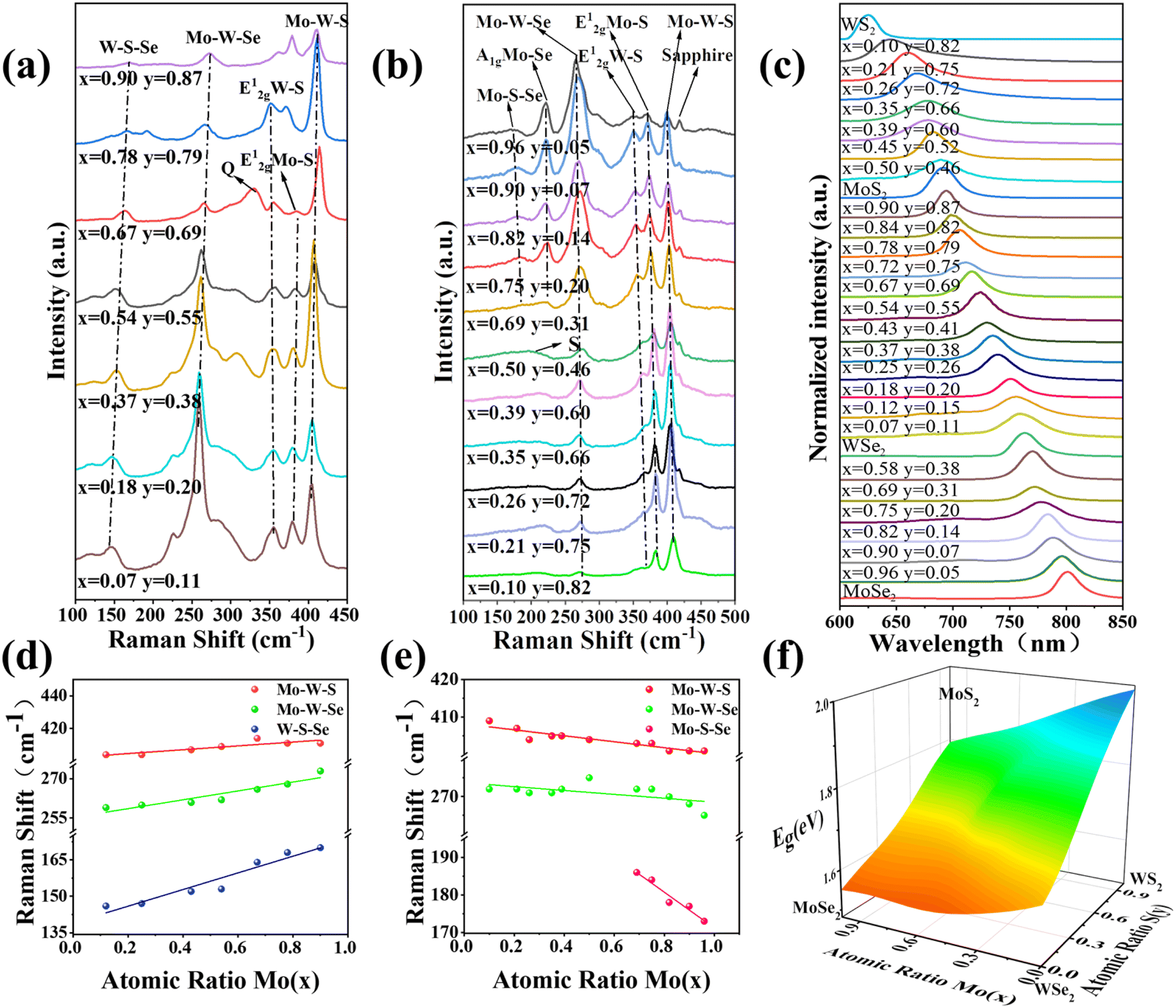 | ||
| Fig. 2 Raman and PL studies of monolayer MoxW(1−x)S2ySe2(1−y) with different ratios. (a) Raman spectra of MoxW(1−x)S2ySe2(1−y) with different weight ratios of MoS2 and WSe2 as growth sources. (b) Raman spectra of MoxW(1−x)S2ySe2(1−y) alloys with different weight ratios of MoSe2 and WS2 as growth sources. (c) Normalized PL spectra of MoxW(1−x)S2ySe2(1−y). (d) Composition-dependent Raman frequencies of MoxW(1−x)S2ySe2(1−y) with different weight ratios of MoS2 and WSe2 as growth sources. (e) Composition-dependent Raman frequencies of MoxW(1−x)S2ySe2(1−y) with different weight ratios of MoSe2 and WS2 as growth sources. (f) 3D band bowing diagram of MoxW(1−x)S2ySe2(1−y). | ||
Different mass ratios of MoSe2 and WS2 powders were selected as the growth source and were varied to synthesize MoxW(1−x)S2ySe2(1−y), thus ensuring the integrity of the experiment. Fig. 2b presents the relevant Raman spectra. The characteristic peak of the out-of-plane vibrational MoSe2-like A1g mode appears at 221 cm−1, whereas the characteristic peak belonging to the Mo–S–Se bond vibrational mode appears in the low-frequency region. The observations contradict the results when the growth sources are MoS2 and WSe2. This finding suggests that the S atoms tend to bond with Mo, Se atoms in the Se-rich environment, and the peak of the Mo–S–Se bond blueshift as the MoSe2/WS2 mass ratio decreases. When x is less than 0.50 and y is less than 0.46, the peak from the Mo–S–Se bond vibrational mode merges with the peak from the MoSe2-like A1g mode into a single peak (S) of reduced intensity. To clarify these results, we determined the trend of the Raman peak frequencies by linear fitting. The characteristic peaks identified in Fig. 2e and S3† vary consistently. Specifically, as the atomic ratio Mo (x) or Se (1−y) decrease, the peak corresponding to the Mo–S–Se blueshifts from 173 cm−1 to 186 cm−1 and then disappears. Similarly, the peak of the Mo–W–Se blueshifts from 265.3 cm−1 to 272 cm−1, and the peak corresponding to Mo–W–S blueshifts from 400.2 cm−1 to 407.5 cm−1. The shifts of the aforementioned Raman peaks are also primarily attributed to the mixed crystal disorder effect.34
PL tests were performed at room temperature to evaluate the optical properties of 25 different atomic ratios of the monolayer MoxW(1−x)S2ySe2(1−y) and 4 pure TMDs. The normalized PL spectra of the 25 different atomic ratios of monolayer TMD alloys and 4 pure TMDs show that all spectra have a single emission peak and no defects or structurally disturbed peaks at lower energies exist, indicating the high quality of the lamellar crystals (Fig. 2c). As the atomic ratio Mo (x) and S (y) changes, the position of the PL single peak continuously blueshifts from 1.99 eV (623 nm) to 1.55 eV (800 nm). The results clarify that the band gaps of quaternary alloys can be adjusted substantially within a range bounded by the band gaps of MoSe2 and WS2 by varying the weight ratio of the growth source. Changes in the trends of band gaps can be described more intuitively. Fig. 2f shows the 3D band bowing diagram of the monolayer MoxW(1−x)S2ySe2(1−y). The peak position of the alloy exhibits a nonlinear variation with the atomic ratio Mo (x) or S (y). This nonlinear peak variation is also called a “bowing effect” and has also been reported in other 2D TMD alloys,23,24,34 mainly attributed to crystal mismatch.
To investigate the homogeneity of the as-grown monolayer MoxW(1−x)S2ySe2(1−y), we performed Raman mapping characterization of the monolayer Mo0.82W0.18S0.28Se1.72 (Fig. 3a–c). The corresponding variation intensities at frequencies of 179 cm−1 (red), 270 cm−1 (green), and 404 cm−1 (blue) are Mo–S–Se, Mo–W–Se, and Mo–W–S, respectively. The consistency of the intensity confirms the homogeneous distribution of the component and stress in the isolated triangular flake, further indicating the uniform distribution of Mo, W, S, and Se in the lattice of the monolayer MoxW(1−x)S2ySe2(1−y). In addition, we recorded randomly selected Raman and PL spectra at four different alloy TMD domains from 1 to 4 in the substrate (Fig. 3d). The Raman and PL peaks at different domains on sapphire substrate are almost identical, which is highly indicative of their thickness and compositional consistency of as-grown monolayer MoxW(1−x)S2ySe2(1−y) on sapphire substrate (Fig. 3e and f).
 | ||
| Fig. 3 Homogeneity characterization of the monolayer MoxW(1−x)S2ySe2(1−y). (a–c) Raman (180 cm−1, 270 cm−1, 418 cm−1) intensity mappings of monolayer Mo0.82W0.18S0.28Se1.72 alloy. (d) Typical OM image of monolayer Mo0.82W0.18S0.28Se1.72 alloy on sapphire substrate. (e and f) The corresponding Raman and PL spectra at four points measured from the substrate in (a). | ||
To further study the PL characteristics of the as-grown sample with different atomic ratios, we used the density functional theory (DFT) and the Vienna Ab Initio Simulation Package,48 together with the projector augmented wave (PAW)49 method, to evaluate variations in the energy band gap. Fig. 4a–c present the top and side views of the atomic structures of 3 monolayer MoxW(1−x)S2ySe2(1−y) with different atomic ratios. TMDs such as 2H-MX2 (M = Mo, W; X = S, Se) are perfect hexagonal symmetric structure crystals; thus, the mutual doping of two TMDs only slightly affects the respective intrinsic hexagonal lattice structure. Consequently, the structure of as-grown alloys remains hexagonal. Fig. 4d–f show the energy band structure diagrams of 3 monolayer MoxW(1−x)S2ySe2(1−y) with different composition. According to DFT calculations, all structures exhibit a direct band gap and the band gap values are 1.57, 1.62, and 1.72 eV, respectively, slightly lower than the experimental values (1.58, 1.66 and 1.80 eV). Meanwhile with increasing W and S atomic ratios, the calculated band gap of MoxW(1−x)S2ySe2(1−y) continues to increase, which trend is consistent with the experimental results.34,49
 | ||
| Fig. 4 DFT calculations of the monolayer MoxW(1−x)S2ySe2(1−y). Optimized top and side view structures of (a) Mo0.82W0.18S0.28Se1.72, (b) Mo0.69W0.31S0.62Se1.38, (c) Mo0.26W0.74S1.44Se0.56. (Mo, blue; W, green; S, yellow; Se, pink). Band structure of (d) Mo0.82W0.18S0.28Se1.72, (e) Mo0.69W0.31S0.62Se1.38, (f) Mo0.26W0.74S1.44Se0.56. | ||
To elucidate the optical properties, we selected the monolayer Mo0.82W0.18S0.28Se1.72 for low-temperature PL measurements (Fig. 5a). Such measurements not only yield the dependence of the band gap on temperature but also help identify the physical mechanisms controlling photoemission. As shown in Fig. 5a, at 300 K, the PL intensity of the monolayer Mo0.82W0.18S0.28Se1.72 decreases significantly relative to that at low temperatures. Generally, the luminescence peak of the alloy widens, and the luminescence intensity decreases as the temperature increases (Fig. 5b). This behavior is due to the exponential enhancement of the nonradiative electron–hole complexation process, which reduces the probability of a radiative transition. As shown in Fig. 5a and c, as temperature increases, the PL peak position is red-shifted, which is typically observed in most semiconductor materials.27 This shift primarily results from dynamic electron–phonon interactions; meanwhile, the role of static lattice expansion is considerably smaller.
 | ||
| Fig. 5 Characterization of the monolayer MoxW(1−x)S2ySe2(1−y). (a) Temperature-dependent PL spectrum of Mo0.82W0.18S0.28Se1.72. (b) Temperature-dependent PL intensity variation plot of Mo0.82W0.18S0.28Se1.72. (c) Temperature-dependent band gap (PL peak energy) variation plot of Mo0.82W0.18S0.28Se1.72. (d–g) XPS spectra of Mo 3d, W 4f, S 2p, and Se 3d core-level binding energies of MoxW(1−x)S2ySe2(1−y). (h) Plot of Mo(S) content obtained by XPS versus weight ratios of MoS2/(MoS2 + WSe2) applied for the prepared MoxW(1−x)S2ySe2(1−y). (i) Plot of Mo (Se) content obtained by XPS versus weight ratios of MoSe2/(MoSe2 + WS2) applied for prepared MoxW(1−x)S2ySe2(1−y). | ||
The composition and chemical state of the monolayer MoxW(1−x)S2ySe2(1−y) were further analyzed by XPS. The Mo 3d, W 4f, S 2p, and Se 3d signals were fitted by splitting the peaks. Splitting the energy levels by spin–orbit coupling also lead to the splitting of the 3d peaks of the Mo4+ oxidation state to form 3d3/2 and 3d5/2 peaks at 233.1 and 230.3 eV, separately (Fig. 5d). The W 4f peak corresponding to the W4+ oxidation state split into 4f5/2 (35.1 eV) and 4f7/2 (32.8 eV) (Fig. 5e). The two characteristic peaks of S2− are located at 2p1/2 (164.1 eV) and 2p3/2 (162.9 eV) (Fig. 5g). In addition, Se 3p3/2 peaks that overlapping with the S 2p region are observed in the S 2p spectrum. Two characteristic peaks are located at 3d3/2 (56.1 eV) and 3d5/2 (55.2 eV) in Se, attributed to the Se2−state (Fig. 5h). We quantified the atomic composition of the alloy by employing the software Advantage 4.2 (Fig. S4–S7 and Table S1, S2†). The atomic ratios of Mo (x) and S (y) in the alloy linearly decrease as the weight ratio of MoS2/(MoS2 + WSe2) is reduced from 0.9 to 0.1 (Fig. 5f). When MoS2 and WSe2 were selected as the growth sources, the pattern of change is almost consistent (Fig. 5i).
To further investigate the sophisticated atomic distribution in the monolayer MoxW(1−x)S2ySe2(1−y), we also examined the monolayer Mo0.82W0.18S0.28Se1.72 by using STEM. In Fig. 6a, the Mo, W sites and the sites of the 2 chalcogenides can be clearly distinguished. To assess the distribution of each atom in the quaternary alloy, we conducted a statistical analysis on a STEM image with dimension of 15 × 15 nm2. First, the types of atoms in the STEM image are distinguished into metal (M) sites and chalcogenide (X2) sites on the basis of intensity and coordination relationships. As shown in Fig. 6b, based on the Z-contrast nature of the STEM image,33,35,47 the intensity histograms of all M sites show two peaks, which are classified as “Mo site” and “W site” regions and denoted by yellow and red. The intensities of the X2 site are shown in Fig. 6c. Similarly, the intensity histograms of all X2 sites reveal three peaks classified as the “SS site,” “SSe site,” and “SeSe site” regions and denoted by green, cyan, and blue, respectively. The distributions of Mo, W, S, and Se are quantified in the 15 × 15 nm2 STEM image. The overall statistical results indicate that 532 SS sites, 850 SSe sites, and 3113 SeSe sites are identified from a total of 4495 X2 sites. The probability of a X2 site being a “SeSe site” (represented as P(SeSe)) is 3113/(532 + 850 + 3113) = 0.693. Similarly, the probabilities of a “SS site” and a “SeSe site,” expressed as P(SS) and P(SSe), are 0.118 and 0.189, respectively. Assuming that SS and SSe are randomly distributed in X2 sites, the total probabilities of P(SS) and P(SSe) also holds for each X2 site. Therefore, the probability of each site distribution can be calculated using the binomial distribution. With the calculation of the SSe site as an example,50
 | (1) |
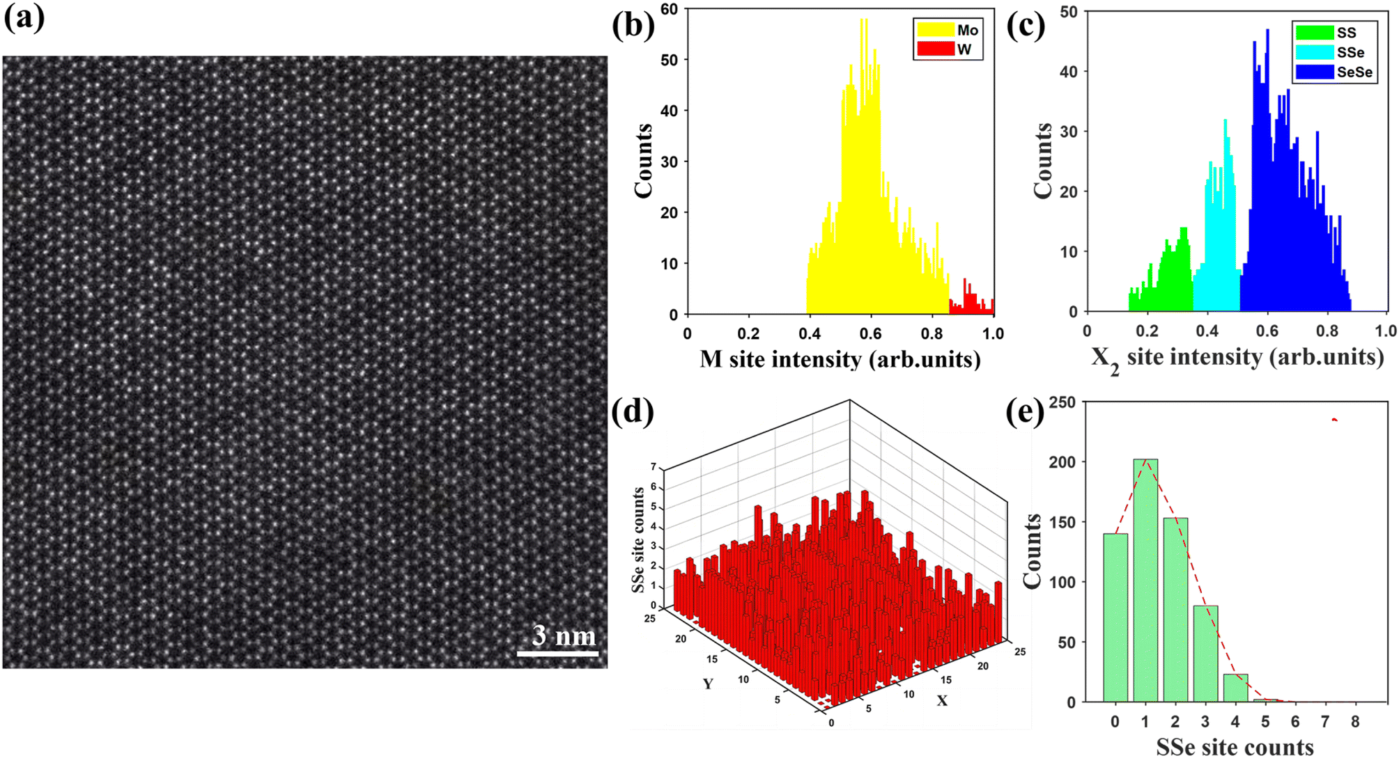 | ||
| Fig. 6 STEM analysis of the monolayer MoxW(1−x)S2ySe2(1−y). (a) HAADF-STEM atomic image of Mo0.82W0.18S0.28Se1.72. Scale bar: 3 nm. (b and c) Histograms of HAADF intensity for metal (M) and chalcogenide (X2) sites in (a), separately. (d) SSe-site distribution histograms in (a). Image was divided into 25 × 25 parts. (e) Corresponding statistical histogram of SSe-site counts in each part of (a). | ||
To further investigate the quality and composition dependence of monolayer alloys, back-gate field effect transistors (FETs) were fabricated using different component alloys on SiO2/Si substrates. Fig. 7a shows the schematic diagram of the FET. Fig. 7b demonstrates the Optical images of Mo0.84W0.16S1.64Se0.36 and Mo0.18W0.72S0.40Se1.60 FETs.
 | ||
| Fig. 7 Electrical measurement of monolayer MoxW(1−x)S2ySe2(1−y). (a) Schematic diagram of a monolayer MoxW(1−x)S2ySe2(1−y) FET. (b) Optical image of prepared FETs. (c) Transfer curve of a monolayer Mo0.84W0.16S1.64Se0.36-based FET. (d) Output curve of a monolayer Mo0.84W0.16S1.64Se0.36-based FET. (e) Transfer curve of a monolayer Mo0.18W0.72S0.40Se1.60-based FET. (f) Output curve of a monolayer Mo0.18W0.72S0.40Se1.60-based FET. | ||
The transfer curves of the monolayer Mo0.84W0.16S1.64Se0.36 alloy FET measured at room temperature, demonstrating the n-type semiconductor transfer behavior and on/off current ratio obtained is about 106 (Fig. 7c). We can calculate the carrier mobility from the transfer (Ids − Vg) curve based on the eqn (2):
| μ = [dIds/dVg] × [L/WCgVds] | (2) |
4. Conclusion
In this study, quaternary monolayer MoxW(1−x)S2ySe2(1−y) were successfully synthesized on sapphire substrates by using a robust liquid phase edge epitaxy (LPEE) method. This technique is a self-limiting growth process, leading exclusively to monolayer MoxW(1−x)S2ySe2(1−y).This synthetic approach achieves the compositionally tunable synthesis of quaternary monolayer MoxW(1−x)S2ySe2(1−y) with well-crystalized and thickness-controlled characteristics, as well as exhibits simplicity, safety, good reproducibility, and homogeneity. By adjusting the mass ratio of MoS2/WSe2 (MoSe2/WS2), monolayer MoxW(1−x)S2ySe2(1−y) with different atomic ratios were obtained. PL results indicate that the band gap can be continuously adjusted from WS2 (1.55 eV) to MoSe2 (1.99 eV) with a change in composition. Meanwhile, monolayer MoxW(1−x)S2ySe2(1−y) has exhibited a continuously broad spectrum, providing a new design idea for obtaining high-performance broad spectrum image sensors. Various characterization techniques exhibit good crystallinity and uniform distribution of components in the grown alloys. By adjusting the alloy composition, the carrier type and carrier mobility of alloy-based field-effect transistors can be systematically modulated. In particular, the adjustable conductivity of MoxW(1−x)S2ySe2(1−y) alloy from n-type to bipolar type is achieved for the first time. The LPEE method described in this study can regulate the atomic ratio of the synthesized materials by controlling the mass ratio of the growth source; in addition, the method has been proven suitable for designing the properties and functions of 2D monolayer materials. This approach can be used to synthesize more 2D semiconductor materials with potential applications in multifunctional electronic devices, catalysis, energy conversion, and spintronic devices.Data availability
The data that support the findings of this study are available from the corresponding author upon reasonable request.Author contributions
You Li: conceptualization, methodology, writing – original draft. Kangkang Wang: software. Junjie Qi and Liming Xie: project administration, supervision, funding acquisition. Yiwen Wang and Junyi Liao: data curation. Wenbin Huan: investigation. Ziyue Qian and Junqi Wang: visualization. Qichao Yang and Honggang Wang: writing – re-view & editing. Sabir Hussain: validation.Conflicts of interest
The authors declare no conflict of interest.Acknowledgements
This work was supported by Beijing Natural Science Foundation (2202030), the Beijing Municipal Science &Technology Commission and the Fundamental Research Funds for Central Universities (FRF-GF-19-001A, FRF-GF-19-002B).References
- J. M. Lu, O. Zheliuk, I. Leermakers, N. F. Yuan, U. Zeitler, K. T. Law and J. T. Ye, Science, 2015, 350, 1353–1357 CrossRef CAS PubMed.
- L. Xu, L. Wang, H. Liu, F. Li, D. Li, Y. Cao, C. Wu, X. Bai and J. Qi, J. Mater. Chem. C, 2021, 9, 5261–5266 RSC.
- X. Wang, B. Wang, Q. Zhang, Y. Sun, E. Wang, H. Luo, Y. Wu, L. Gu, H. Li and K. Liu, Adv. Mater., 2021, 33, e2102435 CrossRef PubMed.
- B. W. Su, X. L. Zhang, B. W. Yao, H. W. Guo, D. K. Li, X. D. Chen, Z. B. Liu and J. G. Tian, Laser Writable Multifunctional van der Waals Heterostructures, Small, 2020, 16, e2003593 CrossRef PubMed.
- J. Ye, W. Chen, Q. Chen, Z. Yu and J. Y. Lee, Acta, 2016, 190, 538–547 CAS.
- J. Hong, C. Wang, H. Liu, X. Ren, J. Chen, G. Wang, J. Jia, M. Xie, C. Jin, W. Ji, J. Yuan and Z. Zhang, Nano Lett., 2017, 17, 6653–6660 CrossRef CAS PubMed.
- P. K. Sahoo, S. Memaran, F. A. Nugera, Y. Xin, T. Díaz Márquez, Z. Lu, W. Zheng, N. Zhigadlo, D. Smirnov, L. Balicas and H. R. Gutiérrez, ACS Nano, 2019, 13, 12372–12384 CrossRef CAS PubMed.
- S. Xie, M. Xu, T. Liang, G. Huang, S. Wang, G. Xue, N. Meng, Y. Xu, H. Chen, X. Ma and D. Yang, Nanoscale, 2016, 8, 219–225 RSC.
- C. Xie, L. Zeng, Z.-x. Zhang, Y. H. Tsang, L.-b. Luo and J. H. Lee, Nanoscale, 2018, 10, 15285–15293 RSC.
- K. L. Seyler, P. Rivera, H. Yu, N. P. Wilson, E. L. Ray, D. G. Mandrus, J. Yan, W. Yao and X. Xu, Nature, 2019, 567, 66–70 CrossRef CAS PubMed.
- S. Fu, K. N. Kang, K. Shayan, A. Yoshimura, S. Dadras, X. Wang, L. Zhang, S. Chen, N. Liu, A. Jindal, X. Li, A. N. Pasupathy, A. N. Vamivakas, V. Meunier, S. Strauf and E. H. Yang, Nat. Commun., 2020, 11, 2034 CrossRef CAS PubMed.
- S. Y. Wang, T.-S. Ko, C. C. Huang, D.-Y. Lin and Y.-S. Huang, Jpn. J. Appl. Phys., 2014, 53, 04EH07 CrossRef CAS.
- Q. Li, X. Zhao, L. Deng, Z. Shi, S. Liu, Q. Wei, L. Zhang, Y. Cheng, L. Zhang, H. Lu, W. b. Gao, W. Huang, C.-w. Qiu, G. Xiang, S. J. Pennycook, Q. Xiong, K. P. Loh and B. Peng, ACS Nano, 2020, 14, 4636–4645 CrossRef CAS PubMed.
- L. Yang, H. Wu, L. Zhang, G. Zhang, H. Li, W. Jin, W. Zhang and H. Chang, ACS Appl. Mater. Interfaces, 2021, 13, 31880–31890 CrossRef CAS PubMed.
- X. Zhou, X. Hu, S. Zhou, H. Song, Q. Zhang, L. Pi, L. Li, H. Li, J. Lü and T. Zhai, Adv. Mater., 2018, 30, 1703286 CrossRef PubMed.
- J. Zhang, W. Xie, J. Zhao and S. Zhang, 2D Mater, 2017, 4, 015038 CrossRef.
- H. Henck, Z. Ben Aziza, D. Pierucci, F. Laourine, F. Reale, P. Palczynski, J. Chaste, M. G. Silly, F. Bertran, P. Le Fèvre, E. Lhuillier, T. Wakamura, C. Mattevi, J. E. Rault, M. Calandra and A. Ouerghi, Phys. Rev. B, 2018, 97, 155421 CrossRef CAS.
- Z. Liu, A. Dibaji, D. Li, S. Mateti, J. Liu, F. Yan, C. J. Barrow, Y. I. Chen, K. Ariga and W. Yang, Mater. Today, 2021, 44, 194 CrossRef CAS.
- F. Chen, S. Ding and W. Su, J. Alloys Compd., 2019, 784, 213 CrossRef CAS.
- A. G. Chanchal, Matter, 2006, 383, 188–193 CAS.
- A. Azizi, Y. Wang, G. Stone, A. L. Elías, Z. Lin, M. Terrones, V. H. Crespi and N. Alem, Nano Lett., 2017, 175, 2802–2808 CrossRef PubMed.
- M. Zhang, J. Wu, Y. Zhu, D. Dumcenco, J. Hong, N. Mao, S. Deng, Y. Chen, Y. Yang, C. Jin, S. H. Chaki, Y.-S. Huang, J. Zhang and L. Xie, ACS Nano, 2014, 87, 7130–7137 CrossRef PubMed.
- H. Li, X. Duan, X. Wu, X. Zhuang, H. Zhou, Q. Zhang, X. Zhu, W. Hu, P. Ren, P. Guo, L. Ma, X. Fan, X. Wang, J. Xu, A. Pan and X. Duan, J. Am. Chem. Soc., 2014, 10, 3756–3759 CrossRef PubMed.
- X. Duan, C. Wang, Z. Fan, G. Hao, L. Kou, U. Halim, H. Li, X. Wu, Y. Wang, J. Jiang, A. Pan, Y. Huang, R. Yu and X. Duan, Nano Lett., 2016, 161, 264–269 CrossRef PubMed.
- S. Susarla, A. Kutana, J. A. Hachtel, V. Kochat, A. Apte, R. Vajtai, J. C. Idrobo, B. I. Yakobson, C. Tiwary and P. M. Ajayan, Adv. Mater., 2017, 29, 1702457 CrossRef PubMed.
- Z. Wang, X. Zhao, Y. Yang, L. Qiao, L. Lv, Z. Chen, Z. Di, W. Ren, S. J. Pennycook, J. Zhou and Y. Gao, Small, 2020, 16, e2000852 CrossRef PubMed.
- S. Tongay, J. Zhou, C. Ataca, K. Lo, T. S. Matthews, J. Li, J. C. Grossman and J. Wu, Nano Lett., 2012, 12, 5576–5580 CrossRef CAS PubMed.
- Z. Liu, M. Amani, S. Najmaei, Q. Xu, X. Zou, W. Zhou, T. Yu, C. Qiu, A. G. Birdwell, F. Crowne, R. Vajtai, B. I. Yakobson, Z. Xia, M. Dubey, P. M. Ajayan and J. Lou, Nat. Commun., 2014, 5, 5246 CrossRef PubMed.
- Y. Y. Hui, X. Liu, W. Jie, N. Y. Chan, J. Hao, Y. T. Hsu, L. J. Li, W. Guo and S. P. Lau, ACS Nano, 2013, 78, 7126–7131 CrossRef PubMed.
- S. B. Desai, G. Seol, J. S. Kang, H. Fang, C. Battaglia, R. Kapadia, J. W. Ager, J. Guo and A. Javey, Nano Lett., 2014, 148, 4592–4597 CrossRef PubMed.
- T. M. G. Mohiuddin, A. Lombardo, R. R. Nair, A. Bonetti, G. Savini, R. Jalil, N. Bonini, D. M. Basko, C. Galiotis, N. Marzari, K. S. Novoselov, S. DUTTASINHA and A. C. Ferrari, Phys. Rev. B, 2009, 79, 205433 CrossRef.
- E. V. Castro, K. S. Novoselov, S. V. Morozov, N. M. R. Peres, J. L. L. dos Santos, J. Nilsson, F. Guinea, S. DUTTASINHA and A. H. C. Neto, Phys. Rev. Lett., 2007, 99, 216802 CrossRef PubMed.
- E. V. Castro, K. S. Novoselov, S. V. Morozov, N. M. R. Peres, J. L. L. dos Santos, J. Nilsson, F. Guinea, S. DUTTASINHA and A. H. C. Neto, Adv. Mater., 2014, 26, 2648 CrossRef PubMed.
- Q. Fu, L. Yang, W. Wang, A. Han, J. Y. Huang, P. Du, Z. Fan, J. Zhang and B. Xiang, Adv. Mater., 2015, 27, 4732 CrossRef CAS PubMed.
- F. Cui, Q. Feng, J. Hong, R. Wang, Y. Bai, X. Li, D. Liu, Y. Zhou, X. Liang, X. He, Z. Zhang, S. Liu, Z. Lei, Z. Liu, T. Zhai and H. Xu, Adv. Mater., 2017, 29, 1705015 CrossRef PubMed.
- P. Tang, H. Shu, M. Yang, M. Zhang, C. Sheng, P. Liang, D. Cao and X. Chen, ACS Appl. Nano Mater., 2021, 4, 12609 CrossRef CAS.
- Q. Feng, N. Mao, J. Wu, H. Xu, C. Wang, J. Zhang and L. Xie, ACS Nano, 2015, 9, 7450–7455 CrossRef CAS PubMed.
- K. Ding, Q. Fu, H. Nan, X. Gu, K. K. Ostrikov and S. Xiao, Mater. Sci. Eng., B, 2021, 269, 115176 CrossRef CAS.
- S. Hussain, R. Zhou, Y. Li, Z. Qian, Z. Urooj, M. Younas, Z. Zhao, Q. Zhang, W. Dong, Y. Wu, X. Zhu, K. Wang, Y. Chen, L. Liu and L. Xie, J. Am. Chem. Soc., 2023, 145, 11348–11355 CrossRef CAS PubMed.
- J. Zhou, J. Lin, X. Huang, Y. Zhou, Y. Chen, J. Xia, H. Wang, Y. Xie, H. Yu, J. Lei, D. Wu, F. Liu, Q. Fu, Q. Zeng, C.-H. Hsu, C. Yang, L. Lu, T. Yu, Z. Shen, H. Lin, B. I. Yakobson, Q. Liu, K. Suenaga, G. Liu and Z. Liu, Nature, 2018, 556, 355–359 CrossRef CAS PubMed.
- H. Wang, X. Huang, J. Lin, J. Cui, Y. Chen, C. Zhu, F. Liu, Q. Zeng, J. Zhou, P. Yu, X. Wang, H. He, S. H. Tsang, W. b. Gao, K. Suenaga, F. Ma, C. Yang, L. Lu, T. Yu, E. H. T. Teo, G. Liu and Z. Liu, Nat. Commun., 2017, 8, 394 CrossRef PubMed.
- B. Jin, P. Huang, Q. Zhang, X. Zhou, X. Zhang, L. Li, J. Su, H. Li and T. Zhai, Adv. Funct. Mater., 2018, 28, 1800181 CrossRef.
- M. Acerce, D. Voiry and M. Chhowalla, Nat. Nanotechnol., 2015, 10, 313–318 CrossRef CAS PubMed.
- D. Voiry, A. D. Mohite and M. Chhowalla, Chem. Soc. Rev., 2015, 44, 2702–2712 RSC.
- Y. H. Lee, L. Yu, H. Wang, W. Fang, X. Ling, Y. Shi, C.-T. Lin, J.-K. Huang, M. T. Chang, C. S. Chang, M. S. Dresselhaus, T. Palacios, L. J. Li and J. Kong, Nano Lett., 2013, 13, 1852–1857 CrossRef CAS PubMed.
- H. Li, X. Wu, H. Liu, B. Zheng, Q. Zhang, X. Zhu, Z. Wei, X. Zhuang, H. Zhou, W. Tang, X. Duan and A. Pan, ACS Nano, 2017, 11, 961–967 CrossRef CAS PubMed.
- M. B. Sreedhara, Y. Miroshnikov, K. Zheng, L. Houben, S. Hettler, R. Arenal, I. Pinkas, S. S. Sinha, I. E. Castelli and R. Tenne, J. Am. Chem. Soc., 2022, 144, 10530–10542 CrossRef CAS PubMed.
- J. P. Perdew, K. Burke and M. Ernzerhof, Phys. Rev. Lett., 1996, 77, 3865–3868 CrossRef CAS PubMed.
- G. Kresse and D. P. Joubert, Phys. Rev. B, 1999, 59, 1758–1775 CrossRef CAS.
- Y. Zuo, C. Liu, L. Ding, R. Qiao, J. Tian, C. Liu, Q. Wang, G.-W. Xue, Y. You, Q. Guo, J. Wang, Y. Fu, L.-Y. D. Liu, X. Zhou, H. Hong, M. Wu, X. Lu, R. Yang, G. Zhang, D. Yu, E. Wang, X. Bai, F. Ding and K. Liu, Nat. Commun., 2022, 13, 1007 CrossRef CAS PubMed.
- R. Jenjeti, R. Kumar, K. Vankayala and S. Sampath, J. Mater. Sci., 2022, 57, 14339 CrossRef CAS.
Footnote |
| † Electronic supplementary information (ESI) available. See DOI: https://doi.org/10.1039/d3ra07065d |
| This journal is © The Royal Society of Chemistry 2023 |