
 Open Access Article
 This Open Access Article is licensed under a
 Creative Commons Attribution 3.0 Unported Licence
Preparation and performance of semiconductor device bonding joints based on Cu@Sn@Ag preform
Honghui Zhang a,
Hongyan Xu*b,
Tianwen Wangb and
Sheng Wangb
a,
Hongyan Xu*b,
Tianwen Wangb and
Sheng Wangb
aXinyang Vocational and Technical College, Xinyang 464000, China. E-mail: zhh20080115@163.com
bMicro-nano Fabrication Technology Department, Institute of Electrical Engineering, Chinese Academy of Sciences, Beijing 100190, China. E-mail: hyxu@mail.iee.ac.cn
First published on 7th December 2023
Abstract
Herein, a 110 A commercial, Si continuous current diode with high heat dissipation power is attached to Cu@Sn@Ag preform, formed by electroplating and physical vapor deposition, and pressed into a preformed sheet under a pressure of 5–10 MPa. The prepared dense three-dimensional network of Cu/Cu3Sn/Ag3Sn joint, based on Cu@Sn@Ag preform obtained using transient liquid-phase diffusion soldering technology, can withstand high temperatures up to 600 °C in power device applications. The mechanical and thermal performance and power cycle reliability of the Cu@Sn@Ag joint are investigated and comparatively analyzed with PbSn5Ag2.5 joints. The results show that the average shear strength of the Cu@Sn@Ag joint is ∼35 MPa, which exceeds that of PbSn5Ag2.5 solder joint, and is similar to that of sintered nano-silver solder joint; the minimum thermal resistance of the corresponding device is ∼0.18 K W−1, near to that of PbSn5Ag2.5 joint. The growth rate of the forward voltage drops below 2% following 150![[thin space (1/6-em)]](https://www.rsc.org/images/entities/char_2009.gif) 000 active power cycles, with a junction temperature difference below 60 °C, meeting the requirements of reliability test standards for vehicle specifications. It is concluded that the performance and power cycle reliability of the Cu@Sn@Ag joint are better than those of the PbSn5Ag2.5 joint.
000 active power cycles, with a junction temperature difference below 60 °C, meeting the requirements of reliability test standards for vehicle specifications. It is concluded that the performance and power cycle reliability of the Cu@Sn@Ag joint are better than those of the PbSn5Ag2.5 joint.
Introduction
A power module, an important energy conversion and control device, is extensively employed in various fields including aerospace, advanced energy, electric vehicles, 5G communication, and photovoltaic power generation. Owing to the rapid development of power modules toward high integration and high-power density, their application temperatures rise to 600 °C. However, the high-temperature-resistant soldering materials employed for power devices have difficulty in exerting the original excellent performance of power devices, particularly for SiC or GaN chips, which pose a formidable challenge for chip soldering materials. Therefore, the development of high-temperature-resistant and high-reliability lead-free soldering materials is imperative for settling this issue.1–4The traditional high-lead-content alloys, including Au–Sn and Sn–Sb–Ag, can easily cause chip warpage and deformation under high chip junction temperatures, and they are unable to meet the requirements of high service temperatures for power devices. Although sintered nanosilver shows comprehensive high performance, the high pressure during the soldering process and the occurrence of silver migration during service easily induce high porosity in the solder layer and deteriorate the joint properties. Additionally, the high cost precludes its popular application. Transient liquid-phase diffusion soldering (TLPS) combines the characteristics of diffusion welding and brazing. Therefore, it is possible to realize low-temperature bonding and high-temperature service and is a viable replacement for high-lead-content alloy solder. Further, it has tremendous prospects in high-temperature packaging for the new-generation power devices represented by SiC.5 Chu et al.6 have employed sandwiched Cu/Sn/Cu and Ni/Sn/Ni material structures and low-temperature TLPS (LT TLPS) technology to prepare pure interfacial intermetallic compound (IMC) joints. These joints are soldered by sandwich-structured metal layers comprising a low-melting-point interlayer, such as Sn or In, and a surface layer of high-melting-point metals, such as Cu, Au, or Zn.7–9 High-temperature-resistant IMCs are formed as the interconnecting joint via liquid–solid interdiffusion, though the long diffusion channel of the Cu/Sn/Cu structure extends the interfacial reaction time and makes it difficult to extend the interface layer thickness. Further, pure IMC joints increase the elastic modulus and reduce the fracture toughness, which are not conducive to reliable running at high temperatures.10 For these challenges, composite-powder-solder-paste-based TLPB technology for the preparation of IMC high-temperature joints has been extensively studied.11–13 This technology is advantageous as the Cu/Sn particles are uniformly mixed and fully intercontacted, and the molten Sn completely infiltrates the Cu particles, which significantly shortens the diffusion channel and strengthens the reaction kinetics. Subsequently, the isothermal diffusion alloying reaction generates homogeneous Cu6Sn5/Cu3Sn compounds. H. Grave et al.14 successfully prepared complete Cu6Sn5 and Cu3Sn joints with a joint thickness below 10 μm by employing this technology, and the thermoelectric properties of the joint are comparable to those of pure silver. However, one of the challenges with this technology is that the structure of the above-prepared high-temperature-resistant joints persists as the pure IMC phase, with high elastic modulus, poor stress absorption capacity, and susceptibility to brittle fracture at the joint interface. Further, challenges that reduce the reliability have not been overcome yet.15–17 Therefore, the joint structure needs to be improved to strengthen the toughness of the joint.
To address these challenges, a dense core–shell structure of Cu@Sn@Ag preform has been developed via electroplating and physical vapor deposition using low-cost Cu particles with a high thermal and electrical conductivity. By refining the micro- and nanometer Cu particle size and the thickness of the Sn/Ag coating layer, the structure, strength, and toughness of the soldering joint can be controlled. This provides an important theoretical basis for the preparation of high-temperature-resistant joint technology via TLPS of the Cu/Sn/Ag system. The thermal, mechanical, and electrical performance of the assembled Si device has been tested and compared with those of the commercial PbSn5Ag2.5 preform to verify the reliability of the Si device assembled with the Cu@Sn@Ag preform.
Materials and methods
Preparation of Cu@Sn@Ag preform
Three kinds of Cu powder, procured from Beijing Institute of Nonferrous Metals, with different particle sizes of <15, 15–25, and 25–50 μm, were selected and mixed according to the mass ratio of 1:3:2 and deoxidized with ethanol hydrochloric acid solution. Further, the activated Cu powder was uniformly and densely plated with a 2–3 μm-thick Sn layer in a prepared solution containing stannous methyl sulfonic acid, methylsulfonic acid, resorcinol, and emulsifier. Subsequently, the Cu@Sn core–shell powder was prepared after ultrasonic cleaning with deionized water and ethanol 3–5 times before being dried in an oven. Next, the prepared Cu@Sn core–shell powder was coated with a 1–2 μm-thick Ag layer outside the Sn layer through physical vapor deposition (PVD) method to obtain the Cu@Sn@Ag composite powder. Finally, the Cu@Sn@Ag particles were compressed under a pressure of 10 MPa for 5 min to obtain the preform with dimensions of φ 9 mm × 100 μm.
Preparation of Cu@Sn@Ag TLPS high-temperature-resistant joint
To improve the consistency of the interconnection interface between the preform and the Si chip, an additional layer of Sn (1–2 μm) was plated on the surface of the preform. Further, the flux was dripped on the surface of the Direct Bond Copper (DBC) board to prevent the substrate oxidization during the welding process. The Si chip, preform, and DBC board were fixed with a fixture and placed in a welding furnace. The joint, comprising a dense three-dimensional network of Cu/Cu3Sn/Ag3Sn, was obtained after heating at 280 °C for 20 min. The schematic configuration of the preform and joint preparation is shown in Fig. 1.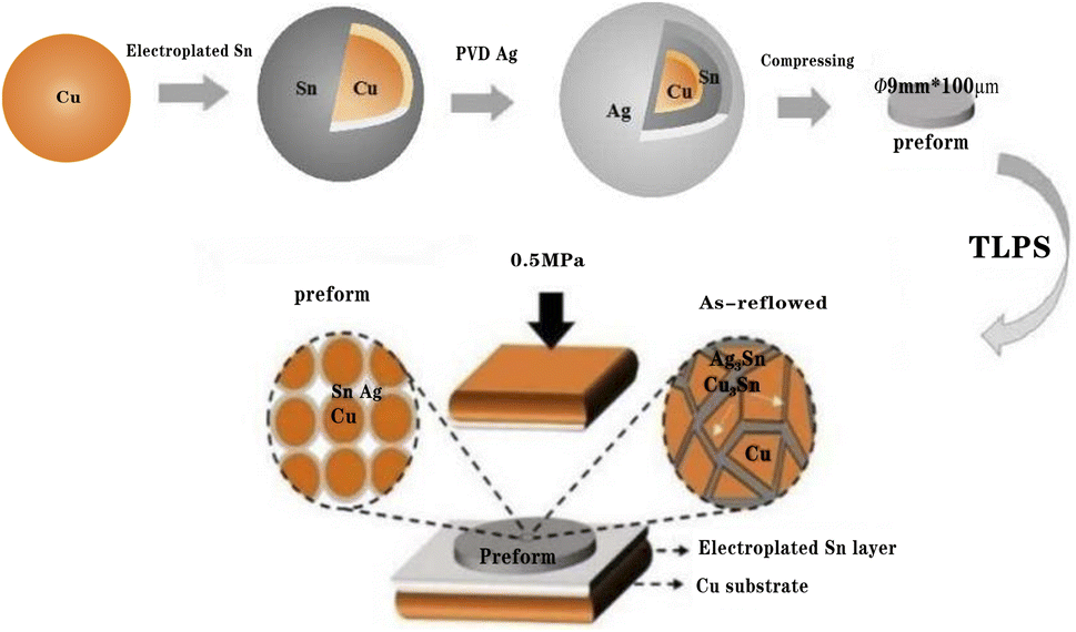 | ||
| Fig. 1 Schematic configuration of the preform and joint preparation. | ||
Following the soldering process, the flux residue on the surface of the Si chip was ultrasonically cleaned in ethanol, and 6–8 aluminum wires were welded using ultrasonic assistance on the surface of the chip to complete the assembly of the Si device. Photographs of the assembled Si chips are displayed in Fig. 2. The entire Si device consists of six layers, namely, the layers of lower copper-clad DBC, DBC ceramic, upper copper-clad DBC, preform, and chip, besides the Al bonding line from bottom to top.
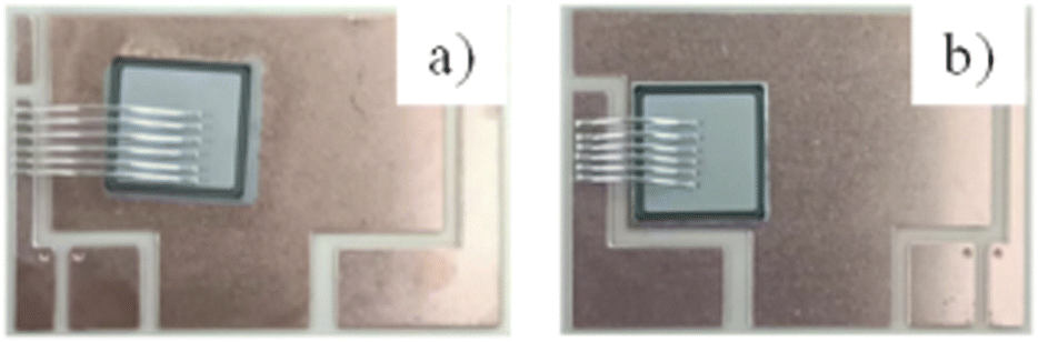 | ||
| Fig. 2 Photographs of Si chips assembled using different solders. (a) Cu@Sn@Ag preform welding. (b) Commercial PbSn5Ag2.5 preform welding. | ||
Results and discussion
Composition and morphology of Cu@Sn@Ag core–shell structure powder
The surface morphology and cross-sectional morphology of the Cu@Sn@Ag powder prepared via PVD after electroplating are depicted in Fig. 3a and b. The Cu@Sn@Ag powder is silver–white, and the Sn shell is covered uniformly on the Cu core with a thickness of ∼2–3 μm, whereas the outer Ag shell with a thickness of ∼1–2 μm is uniformly coated on the surface of the Cu@Sn powder. The core–shell structure of the Cu@Sn@Ag powder has been proved using energy dispersive X-ray spectroscopy (EDX) line-scanning analysis at the Ag–Sn–Cu interface; the elements Cu, Sn, and Ag were detected via EDX and X-ray diffraction analysis (XRD), as shown in Fig. 3c and d. There are no intermetallic compounds such as Cu6Sn5/Cu3Sn/Ag3Sn in the interfacial layer, indicating that no reactions of Cu, Sn, and Ag occurred during electroplating and PVD, which are beneficial for the preparation of dense three-dimensional network structure joints with IMC-reinforced Cu particles.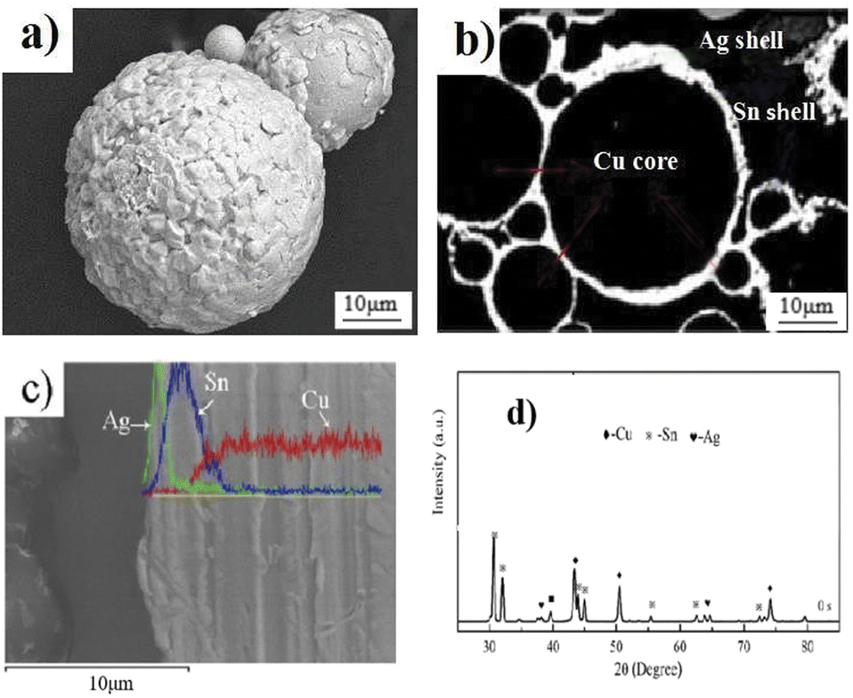 | ||
| Fig. 3 (a) Surface morphology, (b) profile morphology, (c) EDX results, and (d) XRD for of Cu@Sn@Ag core–shell structure powder. | ||
Phase composition evolution and micromorphology of three-dimensional network structure of Cu@Sn@Ag TLPS joints
The Cu@Sn@Ag composite powder was subjected to transient liquid-phase heat treatment at 280 °C for different holding times, and the phase evolution of the Cu@Sn@Ag preform at different holding times was characterized by XRD. As shown in Fig. 4, Cu, Ag, and Sn peaks were detected in the XRD patterns before the transient liquid-phase sintering process. After the preform was heated at 280 °C for 30 s, the Sn phase in the interface was completely consumed, with some generating Cu6Sn5 around Cu particles and the rest reacting with molten Sn to generate Ag3Sn grains. As the reaction time prolonged, the scalloped Ag3Sn grains continued to grow and underwent a solid phase diffusion process before densifying the interface microstructure. When the isothermal solidification time was 2400 s, the reaction was complete, and there was no Cu6Sn5 phase in the interface bulk phase except Ag3Sn, Cu3Sn, and Cu phases. Finally, the three-dimensional network structure Cu@Cu3Sn@Ag3Sn joint with high thermal stability was formed, as shown in Fig. 5. Further, the Cu particles were wrapped by a Cu3Sn layer with a thickness of 1–3 μm, and the outer network structure is a dense Ag3Sn phase with a thickness of 2–3 μm, and no observable holes were found in the local amplification region.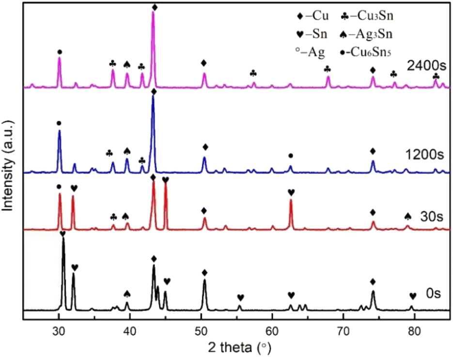 | ||
| Fig. 4 XRD results of the Cu@Sn@Ag preform TLPS for 0 s, 30 s, 1200 s, and 2400 s at 280 °C. | ||
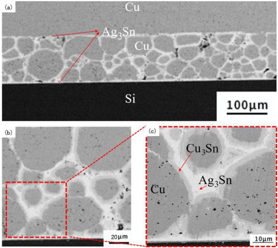 | ||
| Fig. 5 Cross-sectional morphology of Si chips bonded with Cu@Sn@Ag preform at 280 °C for 20 min: (a) overall morphology of the weld seam, (b) partial view of the joint structure, and (c) distribution of Cu/Cu3Sn/Ag3Sn phases in the joint. | ||
Mechanical, thermal and electrical characteristics of the Cu@Sn@Ag TLPS joint
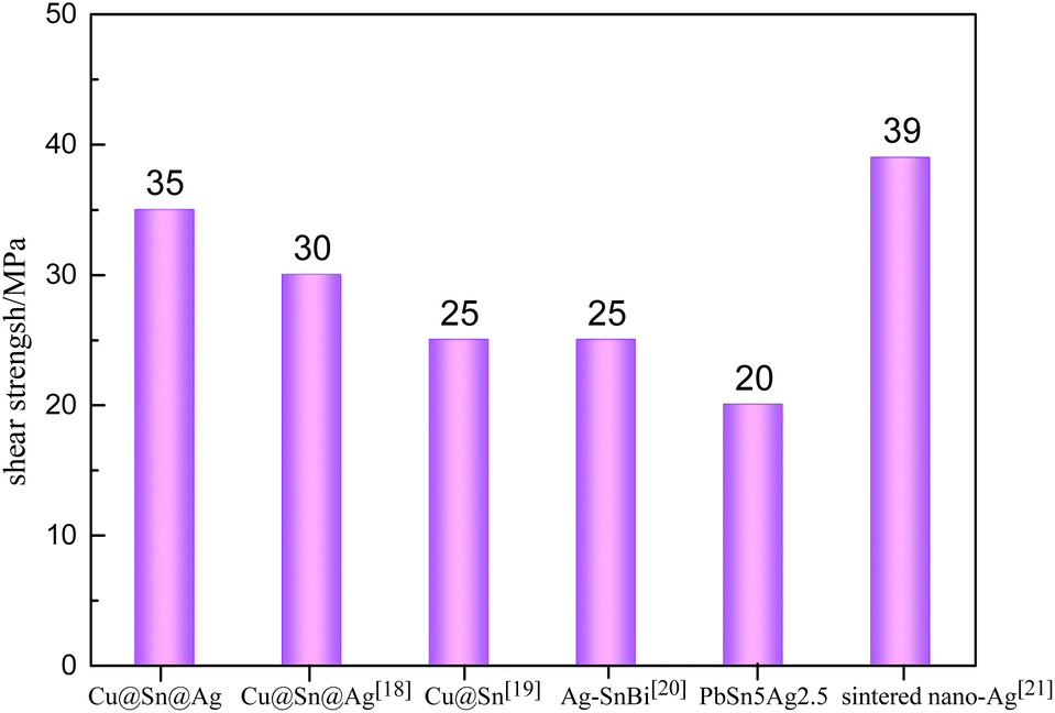 | ||
| Fig. 6 Comparison of shear strength of Cu@Sn@Ag preform and other solders. | ||
The superior shear strength was attributed to the unique cladding structure of the Cu@Sn@Ag solder. This structure shortens the Cu/Sn/Ag element interdiffusive channel, accelerating the formation of Cu3Sn and Ag3Sn interfacial metallic compounds. This continuous transformation from Cu6Sn5 to Cu3Sn ultimately yields a dense three-dimensional network structure of Cu3Sn/Ag3Sn/Cu during the welding process with a short dwelling duration; this improves the strength and toughness of IMC joints. Moreover, the Sn layer electroplated on both sides of the preform catalyzes the reaction between the solder joint, DBC substrate, and copper block, improving the interface density and solving the problem of poor coplanarity. The strength of the welding layer can be increased by employing one material that produces compressive stress, whereas the other material produces equal tensile stress. Finally, the obtained welding layer of Cu@Sn@Ag can improve the reliability of device in high-temperature and high-power regions.
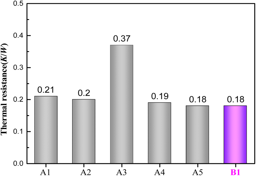 | ||
| Fig. 7 Thermal resistance of Si devices based on different solders (A1–A3: unoptimized Cu@Sn@Ag preform; A4, A5: optimized Cu@Sn@Ag preform; B1: PbSn5Ag2.5 preform). | ||
Fig. 8a and b show the I–V curve of Si devices with different preforms before and after power cycling, respectively. The overlap of the measured I–V curves of devices A4–A9 with the optimized preforms is comparable to that of the devices with the commercial PbSn5Ag2.5 preforms, even with a miniscule change trend and lower forward voltage drop, which proves that the Si devices welded with optimized Cu@Sn@Ag preforms have appreciable quality uniformity.
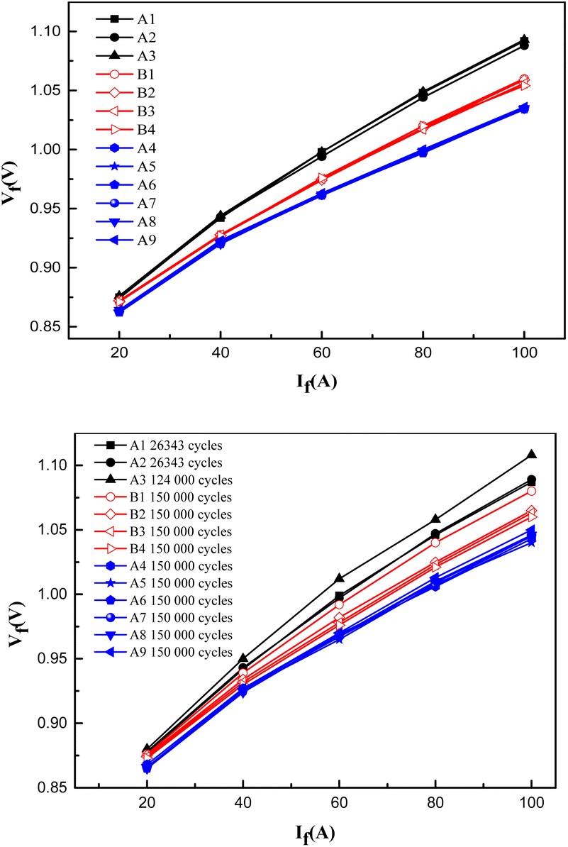 | ||
| Fig. 8 I–V curves of Si devices before and after power cycling (A1–A3: unoptimized Cu@Sn@Ag preform, B1–B4: PbSn5Ag2.5 preform; A4–A9: optimized Cu@Sn@Ag preform). | ||
The input current of 100 A is provided by an external DC power supply. During the power cycle test, the electrical performance and temperature parameters of the device will change, and a 5% increase in forward voltage drop after power cycle is generally employed as the criterion for device failure.25 The parameters of the power cycle test have been set as follows: constant on-time 1 s and off-time 1 s. When the chip temperature reaches the set maximum temperature of 125 °C, the Si device is turned off, and the chip temperature drops to the set minimum temperature of 65 °C, with the assistance of the radiator to complete the cycle process. The continuous cycle temperature difference (60 °C) will affect thermal stress and fatigue, and ultimately the reliability of the device in actual work will be calculated.
Further analysis of the I–V curves, before and after the power cycle, displays that there is little difference in the forward voltage drop of Si devices assembled with different solder pads. The growth rate of the forward voltage drop is below 2% (Fig. 9), before and after the power cycle at 100 A. The stability of the swing amplitude of the forward voltage drop difference of the Si device, which is welded using Cu@Sn@Ag, generally falls below that of the Si device welded using commercial PbSn5Ag2.5. The forward voltage drops of devices A4–A9, before and after the power cycle, falls below those of the four commercial PbSn5Ag2.5 solders, which shows that the optimized Cu@Sn@Ag preforms can meet the reliability requirements for the long-term operation of electronic devices with better application prospects.
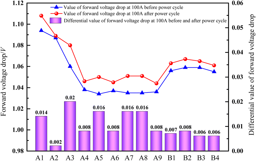 | ||
| Fig. 9 Change in forward voltage drop of Si devices at 100 A before and after power cycling (A1–A3 unoptimized: Cu@Sn@Ag preform; A4–A9: optimized Cu@Sn@Ag preform; B1–B4: PbSn5Ag2.5 preform). | ||
Conclusions
A novel type of Cu@Sn@Ag preform is developed, and a commercial Si chip is welded onto a DBC board using the developed preform and a commercial PbSn5Ag2.5 preform. The effects of different die attachment materials on the thermal, mechanical, and electrical properties and reliability of the Si device have been studied. It is found that the quality of preparation of the Cu@Sn@Ag preform has a tremendous influence on the shear strength and power cycle ability of the whole device.(1) Cu@Sn@Ag dual-core composite powder and its TLPS joint were prepared. The phase composition and micromorphology evolution of the three-dimensional network structure of Cu@Cu3Sn@Ag3Sn dense joint were investigated, which were used to obtain the optimized soldering parameters.
(2) The unique cladding structure of the Cu@Sn@Ag solder makes it possible to obtain a dense three-dimensional network structure of Cu3Sn/Ag3Sn/Cu with excellent mechanical and thermoelectric properties. The shear strength of the welding layer of Cu@Sn@Ag welded with double-sided Sn electroplating can reach 35 MPa, which exceeds that of PbSn5Ag2.5 solder and other welding layers in the same system. The minimum thermal resistance of the corresponding device is ∼0.18 K W−1, close to that of the PbSn5Ag2.5 joint.
(3) The I–V curves of the Si devices assembled by employing the optimized Cu@Sn@Ag and PbSn5Ag2.5 solders are approximately the same before and after 150000 power cycles. The forward voltage drop of the Si device welded with the optimized Cu@Sn@Ag solder is below that of the PbSn5Ag2.5 solder, which demonstrates its higher reliability during use.
Author contributions
Conceptualization, Hongyan Xu; methodology, Hongyan Xu, and Honghui Zhang; resources, Hongyan Xu, and Honghui Zhang; writing—original draft preparation, Honghui Zhang, Tianwen Wang; writing—review and editing, Hongyan Xu, Honghui Zhang, Tianwen Wang and Sheng Wang; supervision, Hongyan Xu, Tianwen Wang and Sheng Wang; project administration, Hongyan Xu; funding acquisition, Hongyan Xu. All authors have read and agreed to the published version of the manuscript.Conflicts of interest
There are no conflicts to declare.Acknowledgements
This work was supported by the Key Research and Development and Promotion of Special Project of Xinyang under Grant No. 20220039; Nature Science Foundation of Beijing under Grant No. 2222083.References
- H. Y. Xu and J. Xu, Fabrication of highly reliable joint based on Cu/Ni/Sn double-layer powder for high temperature application, J. Microelectron. Electron. Packag., 2019, 16(4), 188–195 CrossRef.
- A. Drevin-Bazin, F. Lacroix and J. F. Barbot, SiC Die Attach for High-Temperature Applications, J. Electron. Mater., 2014, 43, 695–701 CrossRef CAS.
- E. GEORGE and M. PECHT, RoHS compliance in safety and reliability critical electronics, Microelectron. Reliab., 2016, 65, 1–7 CrossRef.
- J. R. DAI, J. F. LI and P. AGYAKWA, et al., Comparative thermal and structural characterization of sintered nano-silver and high-lead solder die attachments during power cycling, IEEE Trans. Device Mater. Reliab., 2018, 18(2), 256–265 CAS.
- C. A. Yang, S. Yang and X. Liu, et al., Enhancement of nano-silver chip attachment by using transient liquid phase reaction with indium, J. Alloys Compd., 2018, 762, 586–597 CrossRef CAS.
- K. Chu, Y. Sohn and C. Moon, A comparative study of Cn/Sn/Cu and Ni/Sn/Ni solder joints for low temperature stable transient liquid phase bonding, Scr. Mater., 2015, 109, 113–117 CrossRef CAS.
- S. W. Yoon, M. D. Glover and K. Shiozaki, Nickel-Tin Transient Liquid Phase Bonding Toward High-Temperature Operational Power Electronics in Electrified Vehicles, IEEE Trans. Power Electron., 2013, 28(5), 2448–2456 Search PubMed.
- S. Park, et al., High-Temperature Die Attachment Using Sn-Plated Zn Solder for Power Electronics, IEEE Trans. Compon., Packag., Manuf. Technol., 2015, 5, 902–909 CAS.
- K. Chu, Y. Sohn and C. Moon, A comparative study of Cu/Sn/Cu and Ni/Sn/Ni solder joints for low temperature stable transient liquid phase bonding, Scr. Mater., 2015, 109, 113–117 CrossRef CAS.
- H. H. Zhang and H. Y. Xu, et al., Fabrication of Cu@Sn TLPS joint for high temperature power electronics application, RSC Adv., 2022, 12(45), 29063–29069 RSC.
- K. Guth, N. Oeschler, L. Bower, R. Speckels, G. Strotmann, N. Heuck, S. Krasel and A. Ciliox, New Assembly and Interconnect Technologies for Power Modules, CIPS, Germany, 2012 Search PubMed.
- K. Guth, D. Siepe, J. Görlich, H. Torwesten, R. Roth, F. Hille and F. Umbach, New Assembly and Interconnects beyond Sintering Methods, New Assembly and Interconnects Technology, PCIM, Europe, 2010 Search PubMed.
- J. Watson and G. Castro, A review of high-temperature electronics technology and applications, J. Mater. Sci.: Mater. Electron., 2015, 26, 9226–9235 CrossRef CAS.
- H. Greve, L. Y. Chen, I. Fox, et al., Transient liquid phase sintered attach for power electronics[C], Electronic Components and Technology Conference (ECTC) 2013, IEEE 63rd, IEEE, 2013 Search PubMed.
- M. Brincker, P. K. Kristensen and S. Söhl, et al., Low temperature transient liquid phase bonded Cu-Sn-Mo and Cu-Sn-Ag-Mo interconnects: a novel approach for hybrid metal baseplates [J], Microelectron. Reliab., 2018, 88/89/90, 774–778 CrossRef.
- K. Guth, N. Oeschler, L. Böwer, et al., New assembly and Interconnect Technologies for Power modules[C]∥Proceedings of the 7 Th International Conference on Integrated Power Electronics Systems (CIPS), Nuremberg, Germany, 2012, pp. 1–5 Search PubMed.
- H. Y. Xu, J. Q. Li, et al., Microstructure evolution and properties evaluation of a novel bondline based on Cu@Sn Preform during temperature treatment, ICEPT, 2018, pp. 1709–1715 Search PubMed.
- J. Liu, H. Liu and F. Yu, et al., Cu@ Sn@ Ag core–shell particles preform for power device packaging under harsh environments, J. Mater. Sci.: Mater. Electron., 2021, 32(11), 14703–14714 CrossRef CAS.
- X. Liu, S. He and H. Nishikawa, Low temperature solid-state bonding using Sn-coated Cu particles for high temperature die attach, J. Alloys Compd., 2017, 695, 2165–2172 CrossRef CAS.
- K. F. Muhammad, T. Yamamoto and M. Yoshida, Low temperature and low pressure bonding of plateless Cu–Cu substrates by Ag-based transient liquid phase sintering, J. Mater. Sci.: Mater. Electron., 2017, 28, 9351–9362 CrossRef CAS.
- S. T. Chua and K. S. Siow, Microstructural studies and bonding strength of pressureless sintered nano-silver joints on silver, direct bond copper (DBC) and copper substrates aged at 300 C, J. Alloys Compd., 2016, 687(5), 486–498 CrossRef CAS.
- H. Li, X. Liu, H. Y. Xu and J. Xu, Fabrication of joint based on Cu@Sn@Ag core-shell preform under ambient atmosphere for high-temperature applications, Weld. World, 2022,(66), 1461–1470 CrossRef.
- Y. Avenas, L. Dupont and Z. Khatir, Temperature measurement of power semiconductor devices by thermo-sensitive electrical parameters-A review, IEEE Trans. Power Electron., 2011, 27(6), 3081–3092 Search PubMed.
- P. M. Fabis, D. Shum, and H. Windischmann, Thermal Modeling of Diamond-Based Power Electronics packaging[C]∥ Proceedings of the 15 Th Annual IEEE Semicon-Ductor Thermal Measurement and Management Symposium, San Diego, USA, 1999, pp. 98–104 Search PubMed.
- A. Bajwa, E. Möller and J. Wilde, Die-attachment Technologies for High-Temperature Applications of Si and SiC-Based Power devices[C]∥Proceedings of the 65th Electronic Components and Technology Conference (ECTC), San Diego, USA, 2015, pp. 2168–2174 Search PubMed.
| This journal is © The Royal Society of Chemistry 2023 |