
 Open Access Article
 This Open Access Article is licensed under a Creative Commons Attribution-Non Commercial 3.0 Unported Licence
DFT calculations and giant dielectric responses in (Ni1/3Nb2/3)xTi1−xO2†
Nateeporn Thongyong,
Prasit Thongbai and
Pornjuk Srepusharawoot*
and
Pornjuk Srepusharawoot*
Giant Dielectric and Computational Design Research Group (GD–CDR), Institute of Nanomaterials Research and Innovation for Energy (IN–RIE), Department of Physics, Faculty of Science, Khon Kaen University, Khon Kaen 40002, Thailand. E-mail: spornj@kku.ac.th
First published on 1st November 2023
Abstract
The origins of dielectric responses in Ni2+ and Nb5+ co-doped TiO2 were explored considering intrinsic and extrinsic effects. DFT calculations demonstrated that Ni2+ doping induced oxygen vacancies, while Nb5+ doping generated free electrons. Theoretical predictions indicated complex defect dipoles forming in the rutile structure, contributing to overall dielectric responses. Theoretical calculations also showed a possible linear alignment of Ni2+–2Nb5+ without oxygen vacancies, especially in high doping concentrations. Experimentally, (Ni1/3Nb2/3)xTi1−xO2 ceramics (x = 1%, 2.5%, and 10%) were synthesized. The substantial dielectric response at room temperature, attributed to factors like defect dipoles and grain boundary/surface barrier layer capacitor (GBLC/SBLC) effects, increased with higher doping levels. However, in a temperature range where GBLC/SBLC effects were suppressed, the dielectric response decreased with increased doping, likely due to self-charge compensation between Ni2+–2Nb5+. Notably, (Ni1/3Nb2/3)xTi1−xO2 with x = 2.5% exhibited a high dielectric permittivity of 104 and a low loss tangent of 0.029 at 1 kHz. Moreover, the dielectric permittivity changed by less than ±15% (compared to 25 °C) at 150 °C. This work provides an understanding of the origins of dielectric responses in co-doped TiO2 and optimizes the doping concentration to achieve the best dielectric performance.
1 Introduction
Titanium dioxide (TiO2) and its derivatives have garnered significant attention in the realm of materials science and engineering due to their exceptional dielectric properties and diverse applications.1–3 In the constant pursuit of high performance, high reliability, and low electric power consumption in energy storage and miniaturized devices, there is a growing focus on materials with ‘high’ or ‘giant’ dielectric permittivity.1,4–6 High-quality dielectric materials present an opportunity to develop high-performance capacitor applications.7,8 According to the Electronics Industries Alliance (EIA), class II ceramic capacitors (such as X7R, X8R, and X9R capacitors) are recognized as high-performance capacitors and continue to be in development.7,9 These capacitors demand minimal variation in capacitance with temperature, not exceeding ±15% within a specific range. This requirement presents a significant challenge to overcome.In 2013, Hu et al.1 reported the excellent dielectric properties of (In3+, Nb5+) co-doped TiO2 ceramics (INTO). The remarkable dielectric permittivity (ε′) of approximately 6 × 10⁴ and low loss tangent (tan![[thin space (1/6-em)]](https://www.rsc.org/images/entities/char_2009.gif) δ) of less than 0.02 across a wide frequency and temperature range were achieved. Subsequently, a series of acceptor/donor co-doped TiO2 materials were widely investigated, involving trivalent acceptors and other acceptors. For instance, acceptor dopants (A+, B2+, C3+), isovalent dopant (I4+), and donor dopants (D5+) (A = Ag or Li,10,11 B = Mg, Zn, Sr, Cu or Ca,12–15 C = Al, Sm, Bi, Fe, In, Dy, Ga, Gd, Yb, or Sc,16–20 I = Zr,21 and D = Nb5+, Sb5+, and Ta5+ (ref. 1 and 22–26)).
δ) of less than 0.02 across a wide frequency and temperature range were achieved. Subsequently, a series of acceptor/donor co-doped TiO2 materials were widely investigated, involving trivalent acceptors and other acceptors. For instance, acceptor dopants (A+, B2+, C3+), isovalent dopant (I4+), and donor dopants (D5+) (A = Ag or Li,10,11 B = Mg, Zn, Sr, Cu or Ca,12–15 C = Al, Sm, Bi, Fe, In, Dy, Ga, Gd, Yb, or Sc,16–20 I = Zr,21 and D = Nb5+, Sb5+, and Ta5+ (ref. 1 and 22–26)).
In addition to the exploration of high dielectric performance materials, it is crucial to comprehend the underlying origin of their dielectric properties. The electron-pinned defect dipole (EPDD) mechanism represents a novel approach for elucidating the exceptional dielectric response within co-doped TiO2 systems.1,26,27 Taking into account the substitution of the donor Nb5+ ions for the Ti4+ sites, free electrons are generated, resulting in an increase in ε′ and tanδ. In order to suppress a large tanδ value, the introduction of oxygen vacancies was employed through acceptor doping, particularly with In3+. Doping acceptors or donors onto the Ti4+ sites leads to the formation of internal defect clusters, such as  .1 The dielectric properties of various acceptor/donor co-doped TiO2 systems have been elucidated through the EPDD concept.1,23,28,29 The sole EPDD mechanism still lacks a clear explanation for the overall dielectric properties over a wide frequency–temperature range. Additionally, the internal barrier layer capacitor (IBLC), electron hopping, and surface barrier layer capacitor (SBLC) models are widely employed to elucidate the contribution to the dielectric response.16,17,22,30–33 Based on previous literature, the majority of mechanisms is described in relation to trivalent acceptors. Surprisingly, few studies have explored the dielectric response in the context of bivalent acceptors, even though they also offer remarkable dielectric properties. For instance, (Mg2+, Ta5+),29 (Mg2+, Nb5+),34 and (Zn2+, Nb5+)23 co-doped TiO2 systems exhibit excellent dielectric characteristics. Thus, in this research work, Ni2+ ions have been chosen as acceptors due to their appropriate ionic radius of approximately 69 pm.35 The suitable ionic radius can readily facilitate the formation of EPDDs or remarkable defect dipoles.23,29,34 Unfortunately, the dielectric properties of (Ni2+, Nb5+) co-doped TiO2 have not been reported before.
Defects and their associated dipoles have emerged as crucial factors influencing the dielectric behavior of these materials. Defects, such as vacancies, interstitials, and substitutions, can significantly alter the local electronic structure and charge distribution, thereby inducing dipole moments within the crystal lattice.36 Understanding the impact of these defect-induced dipoles on the dielectric response is paramount for tailoring and optimizing the performance of TiO2-based materials in various technological applications.1,3,36 Density Functional Theory (DFT) has proven to be an indispensable computational tool for investigating the electronic and structural properties of materials at the atomic scale. This approach enables a comprehensive exploration of the underlying mechanisms governing the macroscopic dielectric response observed in TiO2-based materials. Therefore, this study also aims to delve into the realm of defect dipoles and their profound influence on the giant dielectric response exhibited by TiO2-based materials. Furthermore, the experimental data were also designed to support together between the theoretical and experimental results.
In this study, we conducted DFT calculations to predict the potential formation of defect dipoles. Ceramics of (Ni1/3Nb2/3)xTi1−xO2 (with x = 1%, 2.5%, and 10%) were prepared. A high ε′ with low tanδ was achieved at a 2.5% co-doping concentration. The temperature-dependent dielectric properties were investigated over a range of 20 to 483 K. Four relaxations were observed, signifying mechanisms within the dielectric properties. These relaxations provide insights into explaining the origins of the exceptional dielectric properties. Additionally, the contribution of dielectric values to each relaxation was determined to ascertain the most influential mechanisms on dielectric properties. Furthermore, fundamental characteristics were examined, including X-ray diffraction (XRD), Scanning Electron Microscopy (SEM), Raman spectroscopy, and X-ray photoelectron spectroscopy (XPS).
2 Experimental details
All the starting raw materials were obtained from Sigma-Aldrich, which include TiO2 (99.9% purity), NiO (99.99% purity), and Nb2O5 (Sigma-Aldrich, 99.99% purity). The conventional solid-state method formed the powder. Details were provided in the previous published works.24 The powders are neatly ground before being pressed into a disc shape by uniaxial compression at ∼180 MPa. After that, sintered at 1350 °C for 2 h, with a heating rate of 3 °C min−1 in a normal atmosphere, was used to obtain the (Ni1/3Nb2/3)xTi1−xO2 (x = 1%, 2.5% and 10%) ceramics and name as 1%NiNTO, 2.5%NiNTO and 10%NiNTO (xNiNTO).The phase structure of these co-doped ceramics was initially assessed using XRD technique (PANalytical, EMPYREAN). Subsequently, the microstructure of the co-doped ceramics was examined using SEM (SEC, SNE-4500M). For elemental distribution analysis, SEM-mapping was conducted using a focused ion beam-field emission scanning electron microscopy (FEI, QUANTA 450) equipped with energy-dispersive X-ray spectroscopy (EDS). Details of Raman spectroscopy, XPS, and the dielectric measurements were provided in the previous work.24 Before measuring the dielectric properties, we applied silver paste to both sides of the sample and then heated it at 600 °C for 0.5 h. The dielectric response was assessed using a KEYSIGHT E4990A Impedance Analyzer, applying an AC oscillation voltage of 0.5 V. Measurements were conducted over frequency and temperature ranges of 40 to 106 Hz and −258 to 210 °C, respectively.
For computational details, in our works, the Vienna ab initio simulation package (VASP),37 which is a code based on the density functional theory has been used. Additionally, spin-polarized calculations were used. The projector augmented wave approach and the Perdew–Burke–Ernzerhof functional exchange–correlation functional were employed. The energy cutoff and k-point mesh of reciprocal space are 600 eV and 5 × 3 × 3, respectively. For TiO2 structure, rutile phase has been used. Moreover, in these calculations, the 2 × 3 × 5 supercell of this phase was carried out. The chemical formula for this supercell is Ti60O120.
3 Results and discussion
Fig. 1 represents the two possible positions of the oxygen vacancy (Vo) in the Ni doped TiO2 structure. Our calculation results disclosed that total energy when the Vo is at position A is lower than that when the Vo is located at positon B for 0.29 eV. Hence, the Vo is preferably close to the Ni ion. Based on this observation, the oxygen vacancy can be induced by the Ni in this structure. By using the structure with the Vo is at position A as an initial structure, two Nb atoms are inserted into this structure.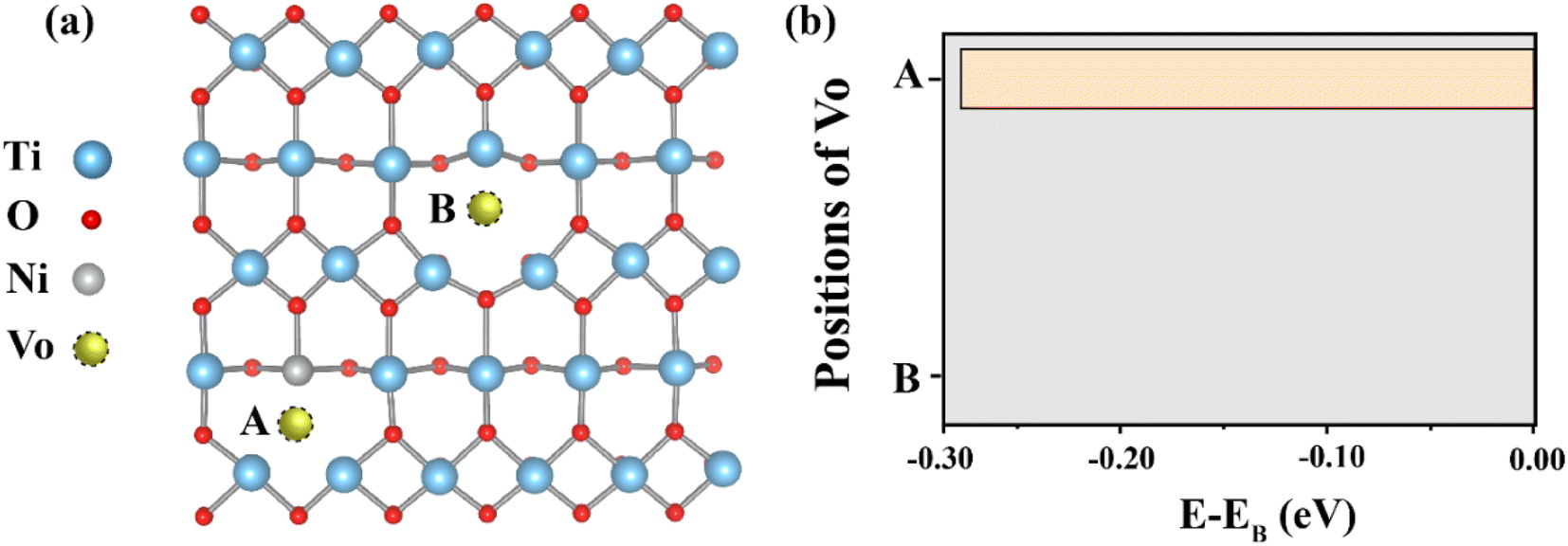 | ||
| Fig. 1 (a) Two possible positions of the oxygen vacancy in the Ni doped TiO2 structure. For position A, the oxygen vacancy is near the Ni, whereas this vacancy does not interact with the Ni when it is located at position B. (b) Total energy corresponds to two positions of the oxygen vacancy. | ||
The total energy of two Nb atoms in the TiO2 with NiVo inside was calculated, as displayed in Fig. 2(a). Four different positions of Nb in the Ni doped TiO2 host are displayed by structures I–IV in Fig. 2(b). According to structure I, two Nb atoms are rather far from both Ni and Vo. For structure II, Nb atoms approach the Vo side. Structure III represents the Nb atoms located at the Ni side. Lastly, two Nb atoms form as the Nb2Ni chain presented by structure IV. The total energy of these four structures is also presented in Fig. 2. We found that total energy of the structure II was the lowest followed by III, I and IV, respectively. Consequently, structure II was a stable structure. In other words, two Nb ions prefer to be close to the Vo.
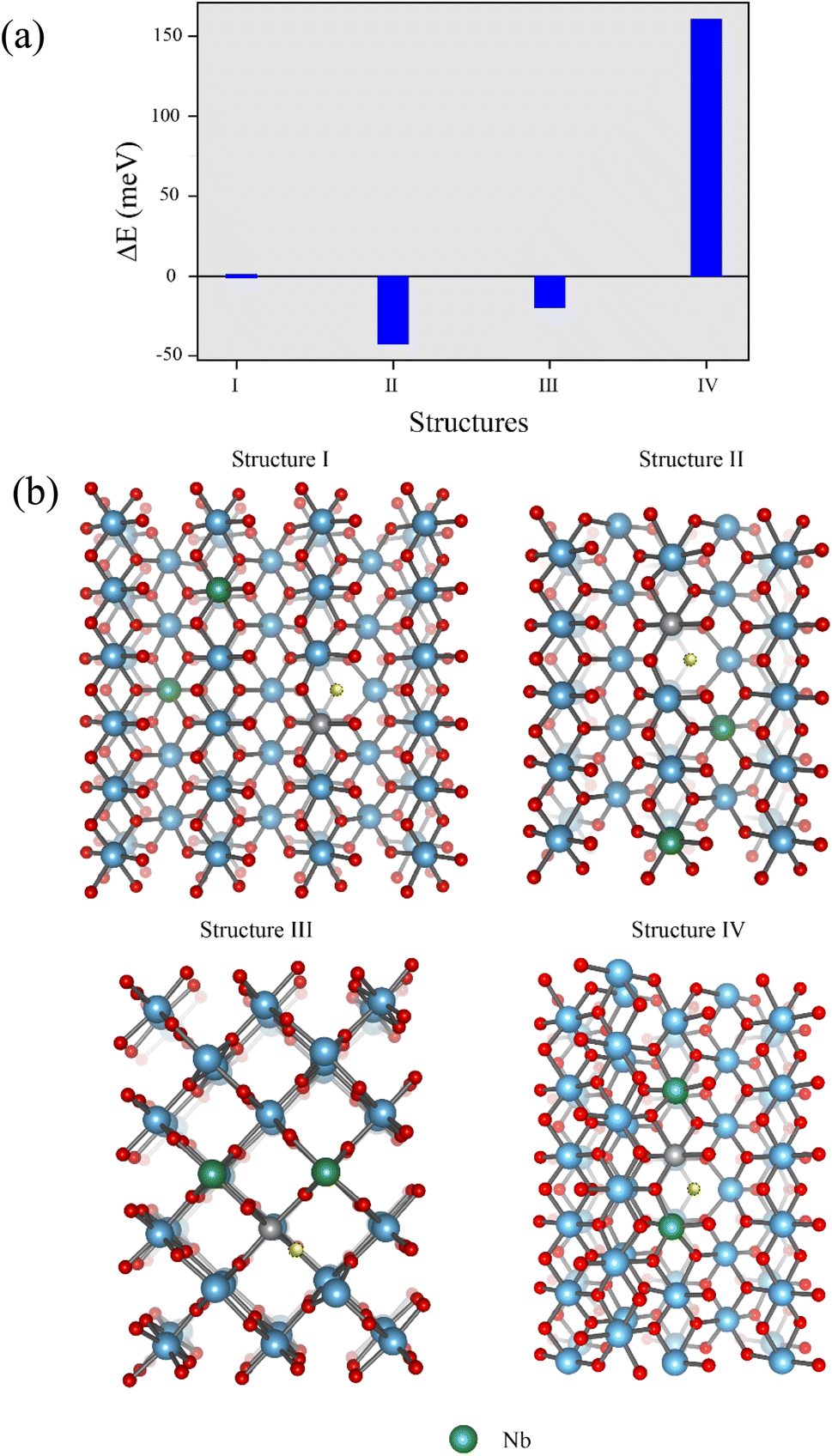 | ||
| Fig. 2 (a) Total energy of two Nb atoms in the TiO2 with NiVo inside. (b) Four different positions of Nb in the Ni doped TiO2: structure I, two Nb atoms are isolated from both Ni and Vo. Structures II and III, two Nb atoms approach the Vo and Ni sides, respectively. Structure IV, Ni and two Nb atoms form as a Nb2Ni chain. | ||
We also investigated the most stable structure of the Ni and Nb co-doped TiO2 without the Vo inside the structure. The total energy for the two distinct configurations of Nb2Ni is illustrated in Fig. 3(a). As shown in Fig. 3(b), for Nb2Ni chain, two Ni atoms are enclosed by two Nb atoms. According to the Nb2Ni triangular structure, as shown in Fig. 3(c), Ni and Nb atoms are located at the corner of the triangle. Total energy corresponding to these structures is presented in Fig. 3(a). Nb2Ni chain is more stable than the Nb2Ni triangle due to lowering in total energy. Hence, based on our calculations, the most stable structure of the Ni and Nb co-doped TiO2 without the Vo is the Nb2Ni chain. In this scenario, there is no requirement for any charge compensations, such as Vo or free electrons.
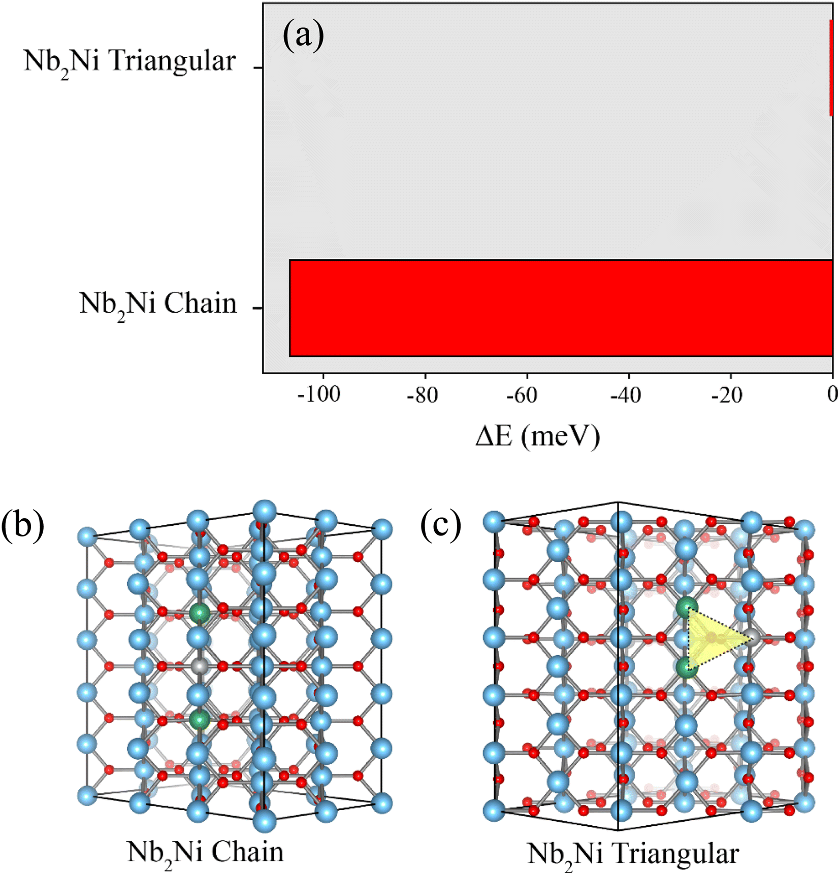 | ||
| Fig. 3 (a) Total energy associated with Nb2Ni in two distinct configurations. (b) Chain configuration of Nb2Ni. (c) Triangular configuration of Nb2Ni. | ||
The XRD patterns of the xNiNTO samples at various concentrations are presented in Fig. 4. All xNiNTO ceramics exhibited a tetragonal unit cell structure with the P42/mnm space group. The primary diffraction peak corresponds to the pure rutile TiO2 crystal structure (JCPDS #21-1276).38,39 No secondary phases are detected, which can be attributed to the close ionic radii of Ni2+ (∼69 pm) and Nb5+ (∼64 pm) to that of Ti4+ (∼60.5 pm), in accordance with the Hume-Rothery rules.18 The lattice parameters of the samples were determined through Rietveld refinement and are detailed in Table 1. The a and c values increase with higher co-doping content. This outcome aligns with observations in other acceptor/donor co-doped TiO2 materials.1,40,41 The substitution of co-dopant Ni2+ and Nb5+ ions at the Ti4+ sites leads to a significant expansion of the lattice parameters. This expansion provides crucial evidence supporting the incorporation of Ni2+ and Nb5+ ions at the Ti4+ sites without the emergence of secondary phases.35 This expansion can be attributed to the larger ionic radii of the dopants compared to Ti4+. It is important to note that the Ti3+, Ti4+,  , Ni2+, and Nb5+ were confirmed to exist in the samples using XPS technique, as shown in Fig. S1 and S2 (ESI†).
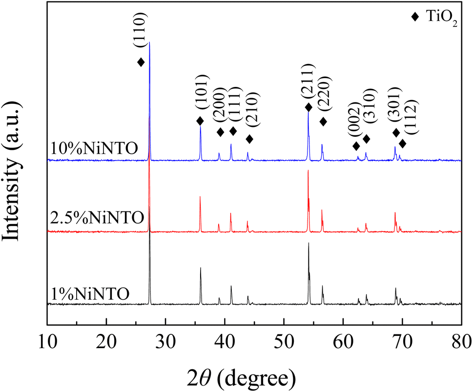 | ||
| Fig. 4 XRD patterns of xNiNTO with various dopant concentrations. | ||
| Sample | Lattice parameters (Å) | Raman shift (cm−1) | Density (g cm−3) | ||
|---|---|---|---|---|---|
| a | c | Eg | A1g | ||
| TiO2 | 4.593(1) | 2.959(3) | 448.3 | 610.6 | 4.23 |
| 1%NiNTO | 4.592(7) | 2.960(8) | 445.9 | 611.2 | 4.20 |
| 2.5%NiNTO | 4.593(2) | 2.960(9) | 444.1 | 613.0 | 4.26 |
| 10%NiNTO | 4.601(9) | 2.966(5) | 441.0 | 614.2 | 4.35 |
To provide further confirmation of the substitution co-doping within the Ti4+ sites, Raman spectroscopy was employed (Fig. 5). Four distinct Raman characteristics (B2g, B1g, Eg, and A1g) are consistent with the rutile TiO2 phase.42 Specifically, the B1g mode corresponds to the O–Ti–O bending vibration, the Eg mode involves oxygen atoms moving out of the crystal lattice along the c-axis, and the A1g mode signifies O–Ti–O stretching vibration.22,42 Generally, the observed shifts in the Raman peaks of rutile TiO2 with varying co-doping concentration suggest changes in the crystal environment due to the incorporation of foreign ions. As depicted in Table 1, the A1g peak demonstrates a shift towards higher wavelengths, signifying the impact of substituted dopants on the O–Ti–O stretching vibration. This shift is attributed to the distinct ionic radii between the dopants and host ions. The Eg peaks of all xNiNTO ceramics exhibit a shift to lower wavelengths with increasing co-doping concentration. This result indicated an increase in Vo concentration.42 The introduction of Ni2+ into the Ti4+ site necessitates a positive charge for charge equilibrium, leading to the generation of Vo according to the equation:
 | (1) |
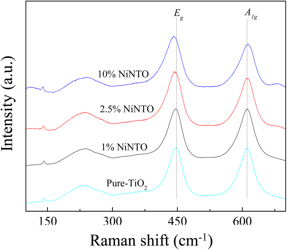 | ||
| Fig. 5 Raman spectra of TiO2 and xNiNTO with various dopant concentrations. | ||
SEM micrographs of the xNiNTO sample are illustrated in Fig. 6(a)–(d). All ceramic specimens exhibited a morphology characterized by smooth-surfaced grains. The average grain sizes for the 1%NiNTO, 2.5%NiNTO, and 10%NiNTO samples are measured and found to be 10.5 ± 4.2, 9.8 ± 4.9, and 4.9 ± 2.3 μm, respectively. As the co-doping (Ni1/3Nb2/3)x increased from 1% to 2.5%, there was a slight change in grain size. However, a notable reduction in grain size was observed when the co-doping concentration rose from 2.5% to 10%. This suggests that Ni2+ and Nb5+ presence hindered grain growth within the samples.43,44 According to previous work,24,45 the mean grain sizes of TiO2 were significantly reduced by factors of 2 and 3 when doped with 1.67 at% Ni2+ and 1 at% Nb5+, respectively. Therefore, the reduction in grain size of the xNiNTO can be attributed to the substitution by both Ni2+ and Nb5+ dopants. For BaTiO3 and CaCu3Ti4O12 doped with high concentrations of Nb5+ or Ta5+,46,47 significant grain growth inhibition was observed. This has been ascribed to the generation of space charges at grain boundaries. During the sintering process, the diffusion rate of O2− across grain boundaries, which contributes to grain growth, is impeded by space charges from accumulated free electrons (e−). This is due to the repulsive force between O2− and e−.
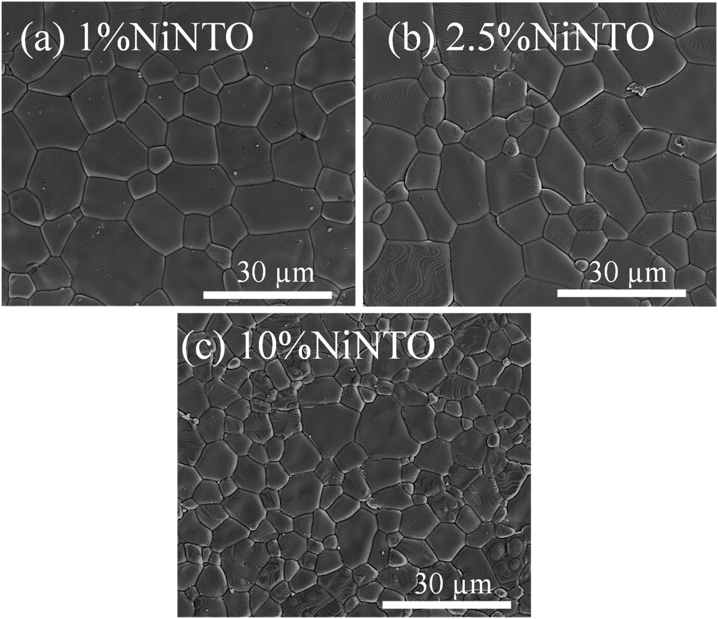 | ||
| Fig. 6 SEM images of (a) 1%NiNTO, (b) 2.5%NiNTO, and (c) 10%NiNTO. | ||
Furthermore, the element on the surface was investigated using the FE-SEM mapping technique, as shown in Fig. 7. The results reveal the elemental distribution of Ti, O, Nb, and Ni on the surface of the 2.5%NiNTO sample. The highest concentration is observed for Ti and O elements, while Ni and Nb exhibit slightly lower contributions, likely attributed to their dopant contents.
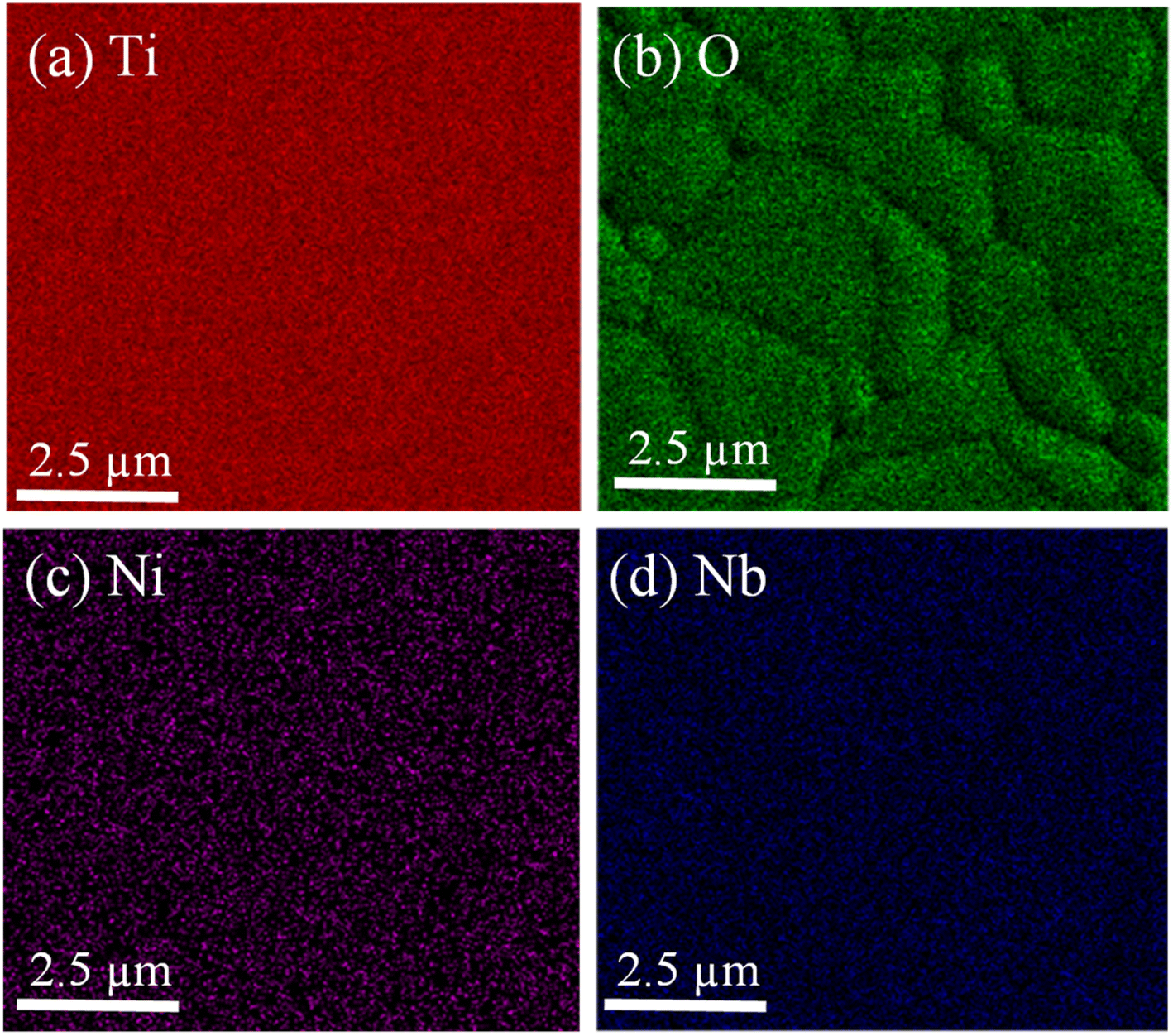 | ||
| Fig. 7 SEM mapping images of 2.5%NiNTO for (a) Ti, (b) O, (c) Ni, and (d) Nb elements. | ||
The frequency-dependent behavior of ε′ and tanδ for the xNiNTO samples is illustrated in Fig. 8(a) and (b), measured at room temperature. The ε′ values for all the samples exhibit a slight dependence on frequency, while the tanδ values show notable sensitivity to frequency variations. Notably, the ε′ value at approximately 30 °C for xNiNTO samples increases with higher co-dopant content. The increase in ε′ with higher co-dopant content is consistent with the behavior observed in similar systems,1 suggesting that the incorporation of Ni2+ and Nb5+ ions can enhance the dielectric response. The ε′ and tanδ values at around 30 °C and 1 kHz for the xNiNTO ceramics are summarized in Table 2. Particularly high ε′ values exceeding 104 were achieved at doping contents of x = 2.5% and 10%. Remarkably, the 2.5%NiNTO composition exhibited promising dielectric properties with an ε′ of approximately 11166 and a tanδ of 0.029 at 1 kHz. Interestingly, at 40 Hz, tanδ was as low as 0.01. This clearly demonstrates that the co-doping of Ni2+ and Nb5+ significantly influences the dielectric properties, potentially due to a range of contributing factors. Additionally, the co-doping content plays a crucial role, evident in the optimal co-doping content of 2.5%. The relationship between co-doping content and dielectric behavior further emphasizes the importance of precise tuning for optimal performance. The comparison of the ε′ and tanδ values at approximately 30 °C and 1 kHz for 2.5%NiNTO and previous works is depicted in Fig. 8(c).12,15,23,24,45,48–50 The comparative results reveal that 2.5%NiNTO, with its high ε′ and tanδ values, shows promise for applications in capacitors. It should be noted that while a high ε′ can be achieved in 5%Nb5+-doped TiO2, the tanδ was significantly large, approximately 0.5.49 On the other hand, 1.67%Ni2+-doped TiO2 offered a low tanδ, but its ε′ is only around 103.24
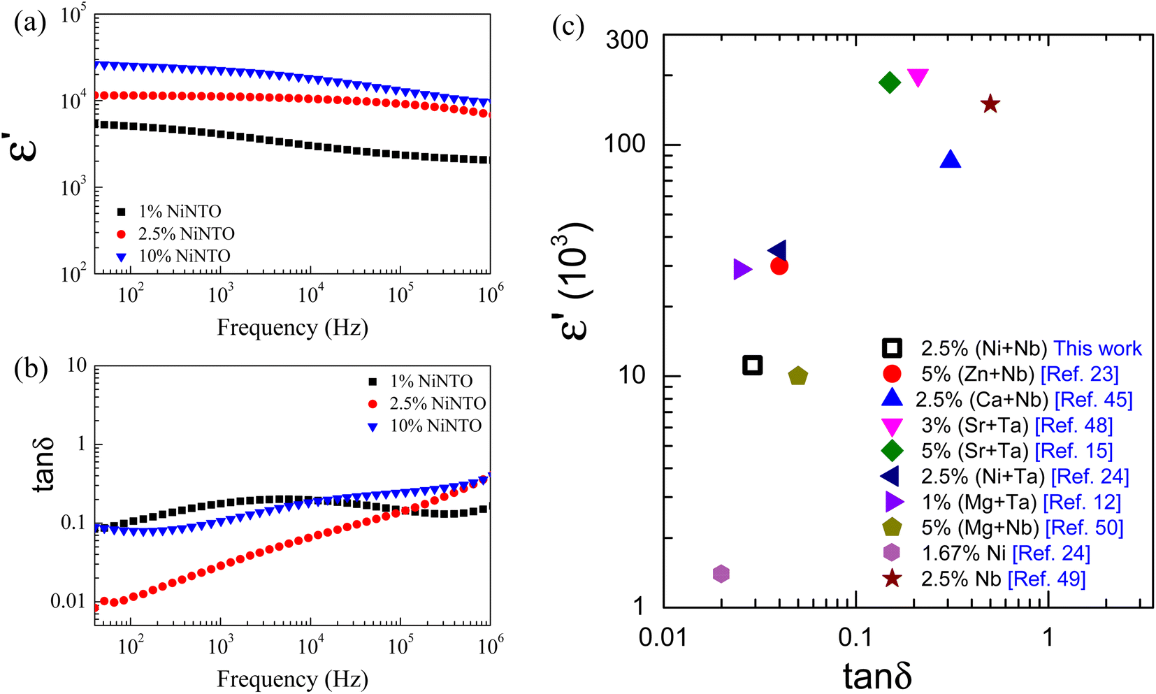 | ||
| Fig. 8 Frequency dependence of dielectric properties of (a) ε′ and (b) tanδ at ∼30 °C for 1%NiNTO, 2.5%NiNTO, and 10%NiNTO. (c) ε′ and tanδ at ∼30 °C and 1 kHz of 2.5%NiNTO compared to previous works. | ||
δ) at 1 kHz, and relaxation activation energies of xNiTTO ceramics
| Sample | Dielectric properties (∼30 °C/1 kHz) | Ea (eV) | |||
|---|---|---|---|---|---|
| ε′ | tanδ |
R1 | R2 | R3 | |
| 1%NiNTO | 4090 | 0.177 | — | — | — |
| 2.5%NiNTO | 11166 |
0.029 | 0.037 | 0.103 | 0.527 |
| 10%NiNTO | 22502 |
0.106 | 0.058 | 0.129 | 0.304 |
Dielectric spectroscopy assessments were performed on both the 2.5%NiNTO and 10%NiNTO ceramic materials across a temperature spectrum of 20 to 483 K. It should be noted that the temperature dependence of ε′ for the 1%NiNTO ceramic was not assessed due to its pronounced tanδ value at lower frequency ranges. These findings are delineated in Fig. 9(a) and (b). The 10%NiNTO variant manifested a heightened temperature sensitivity, evidenced by a considerable augmentation in the ε′ value in response to increasing temperatures. In contrast, the 2.5%NiNTO ceramic demonstrated superior temperature stability, maintaining a relatively constant ε′ value, a trait corroborated by data depicted in Fig. 9(b). Moreover, when comparing the temperature coefficients of ε′ (Δε′/ε′30), the 2.5%NiNTO ceramic exhibits changes within ±15% of the Δε′/ε′30 over a temperature range from 243 to 453 K.
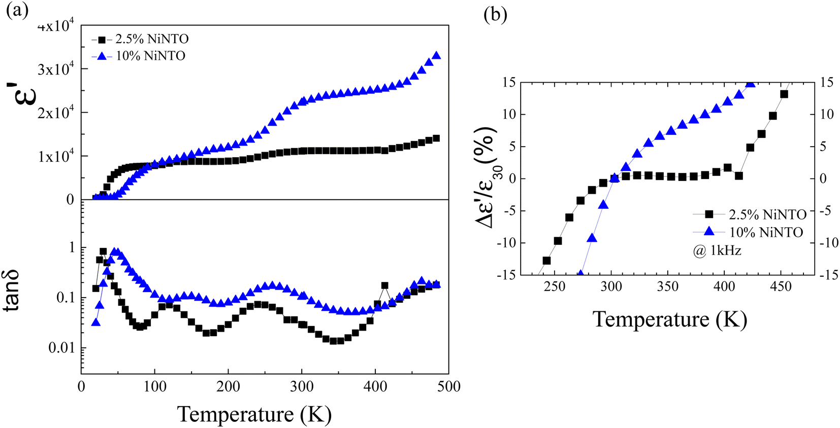 | ||
| Fig. 9 (a) Temperature-dependent behaviors of ε′ and tanδ for ceramics composed of 2.5%NiNTO and 10%NiNTO, measured over a temperature range of 20 to 483 K. (b) Temperature coefficient of ε′ at a frequency of 1 kHz for 2.5%NiNTO and 10%NiNTO. | ||
As shown in Table 2 and Fig. 9(b), among the three samples, the 2.5%NiNTO ceramic displayed both the lowest tanδ value and the most favorable temperature coefficient. Consequently, we selected the 2.5% sample for detailed analysis, with the belief that its properties can be further fine-tuned to better suit capacitor applications. Fig. 10(a) and (b) depict the ε′ and tanδ as functions of temperature and frequency, respectively, showing multiple relaxation responses of the 2.5%NiNTO ceramic. Several dielectric relaxations in the 2.5%NiNTO ceramic were observed, labeled as R1, R2, R3, and R4 in ascending order from low to high temperatures. A step-like decrease in ε′ was accompanied by a shift in the tanδ peak position, which moved to higher frequencies as the temperature increased. This observation signifies the thermally activated dielectric relaxation phenomenon. The R1, R2, and R3 relaxations were evident in the temperature ranges of 20–70 K, 100–180 K, and 190–260 K, respectively. The R4 relaxation emerged at temperatures exceeding 400 K. In xNiNTO ceramics, when we observe an ε′ value around room temperature (∼300 K), it is important to note that there are at least four primary associated polarizations that collaborate to contribute to the dielectric response, resulting in such an ε′ value at 300 K. First, a low ε′ value of roughly 230 below 20 K can be attributed to electronic and ionic polarization. The contributions from R1, R2, and R3 will be discussed in subsequent sections. It should be noted that the contribution from R4 occurs at temperatures exceeding 400 K. Nevertheless, the R4 relaxation will also be described.
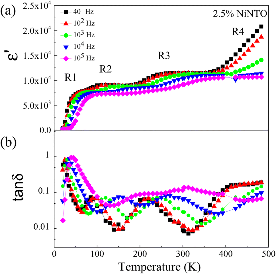 | ||
| Fig. 10 Dielectric relaxation steps in 2.5%NiNTO contributed from different mechanisms of polarizations: (a) ε′ and (b) tanδ as functions of temperature and frequency. | ||
To better understand the physical mechanism underlying the dielectric relaxations, the imaginary part (ε′′ = ε′tanδ) of the complex dielectric permittivity (ε* = ε′ − iε′′) for 2.5%NiNTO as a function of frequency has been plotted in different temperature ranges, as shown in Fig. 11(a)–(c). Generally, the Debye model accounts for the dielectric relaxation using the Arrhenius equation as:
 | (2) |
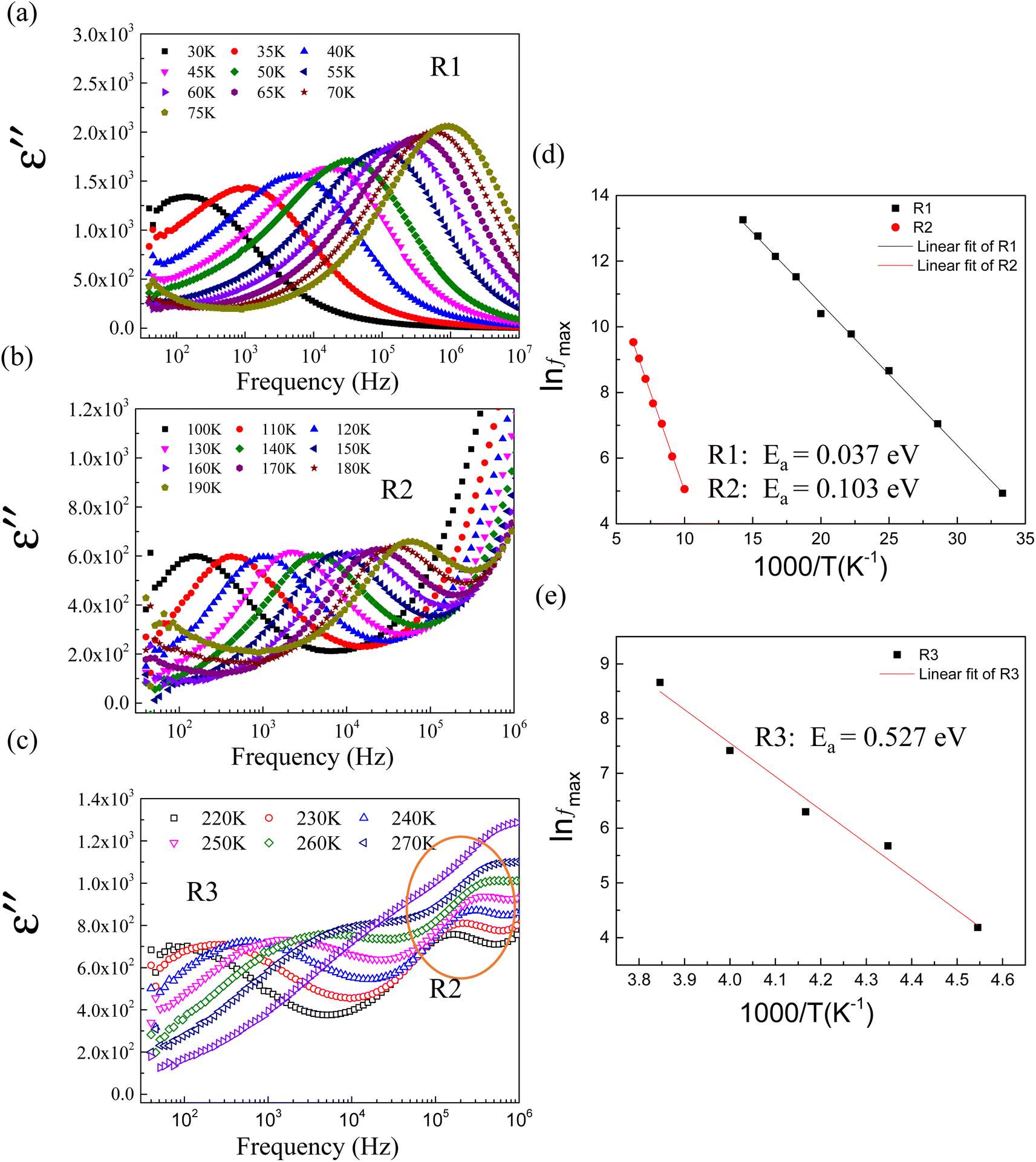 | ||
| Fig. 11 Frequency dependence of ε′′ (ε′′ = ε′tanδ), expanding view of dielectric relaxations in 2.5%NiNTO: (a) R1, (b) R2, and (c) R3. (d) Arrhenius plot for R1 and R2 relaxations. (e) Arrhenius plot for R3 relaxation. | ||
We focused on the contribution of the R1 relaxation to the dielectric response, which was approximately 7.5 × 10³. Fig. 11(a) illustrates the frequency dependence of ε′′ across temperatures ranging from 30 to 75 K, where a distinct ε′′ peak is evident. As the temperature rises, the relaxation peak shifts towards higher frequencies, a characteristic of thermally activated relaxation. The Ea of 0.037 eV was calculated, as shown in Fig. 11(d). This Ea value, being modest, is less than the conduction activation energy within the semiconducting grains. According to the DFT calculations presented in Fig. 1–3, it was theoretically established that defect clusters associated with  and free electrons from Nb5+ were formed, leading to the creation of EPDDs conceptually. Consequently, the R1 relaxation is likely related to the activation or freezing of electrons in defect-dipole clusters. This interpretation aligns with the DFT calculations, which confirm the existence of EPPDs arising from acceptor and donor dopants.51
The R2 relaxation was then characterized. In this study, the formation of some Ti3+ occurred due to the doping of donor ions, while doping with Ni2+ led to the creation of oxygen vacancies. The point defects associated with 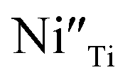 ,
, 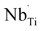 ,
,  and
and  were formed and interconnected, aligning with the configurations predicted by the DFT calculation. A detailed examination of the R2 relaxation is provided in Fig. 11(b). An Arrhenius plot of the relaxation was derived from the linearly fitted curve, as illustrated in Fig. 11(d). The Ea for the R2 relaxation was calculated to be 0.103 eV. This value closely matches the activation energy associated with the movement of free electrons within the semiconducting grains. The Ea value is consistent with findings in +3/+5 co-doped TiO2 and the grain of CCTO.4,52,53 In giant dielectric oxides possessing an IBLC structure, previous studies have demonstrated that the activation energy for dielectric relaxation and the conduction activation energy within semiconducting grains are nearly identical.53,54 Therefore, the origin of the R2 relaxation is attributed to the IBLC effect. The relaxation polarization at the grain boundary, framed by neighboring semiconducting grains, can be accentuated. Additionally, the relaxation time (τ = 1/2πfmax) of the dipole moment for R2 rotates more slowly than that of the R1 relaxation. This can be attributed to the fact that free electrons confined in defect dipoles are more readily moved by the electric force from an applied field (F = qE) than the electron hopping between Ti3+–O2−–Ti4+. The movement of a negatively charged electron is often hindered by the negative charges of the O2− ion. As a result, it takes longer for the electron to move and accumulate at the grain boundary, leading to the production of interfacial polarization. At any given temperature, polarization from the IBLC effect requires a longer duration, indicating a larger relaxation time for R2.
Fig. 11(c) illustrates the relaxation peak of ε′′ occurring below 105 Hz, corresponding to the R3 relaxation. The activation energy for the R3 relaxation, depicted in Fig. 11(e), is 0.527 eV. This value is possibly attributable to the SBLC effect.24,55 Interfacial polarization predominates at the boundary between the outer surface layer and the inner semiconducting core, leading to polarization relaxation.
Additionally, results derived from the fitting of the Arrhenius equation for other co-doped TiO2 contents are presented in Table 1. The mechanism underlying each relaxation remains consistent with that observed in 2.5%NiNTO. Notably, the R1 relaxation increases prominently from a concentration of 2.5% to 10%. These findings suggest that the relaxation of polarized electron confinement within the EPDD structure becomes more challenging to induce as co-doping content rises. This is evidenced by the R1 relaxation in the 10%NiNTO ceramic requiring greater activation energy than its 2.5%NiNTO counterpart.56 This observation aligns with the DFT calculations, which forecast the formation of a linear alignment of Ni2+–2Nb5+ without oxygen vacancies (self-charge compensation) as co-doping content increases. Consequently, the EPDD concentration in the 10%NiNTO ceramic should be diminished compared to the 2.5%NiNTO ceramic. This is attributed to the self-charge compensation mechanism, which negates the formation of free electrons from Nb5+ doping ions.1 The activation energy for the R2 relaxation escalates as co-doping concentration rises, indicating that the R2 relaxation demands more energy under increased co-doping. This can be linked to the anticipated self-charge compensation in the 10%NiNTO ceramic, leading to a reduced concentration of free electrons within the semiconducting grains and  . Thus, relaxation due to the IBLC effect in the 10%NiNTO ceramic, associated with semiconducting grains and insulating grain boundaries, necessitates higher energy. Although the activation energy of the R3 relaxation pertains to the SBLC effect,24 its trend diminishes in the 10%NiNTO ceramic. This suggests a reduced resistivity of the 10%NiNTO ceramic's insulating surface compared to the 2.5%NiNTO. This could be because the active acceptor ions in the 10%NiNTO were mitigated due to the self-charge compensation of Ni2+–2Nb5+. This results in a diminished Schottky barrier height at the interface between the semiconducting inner core and the outer layer.57 Thus, less activation energy is needed for a dielectric response at this Schottky contact. Minimal energy is adequate to surpass a low Schottky barrier height. At elevated temperatures, the movement of
  or oxygen ions becomes feasible, contributing to the dielectric response. Therefore, the R4 relaxation is associated with the DC conduction of
  or O2− ions.5 This research has unveiled critical insights into dielectric relaxation, underscoring the intricate behaviors and mechanisms within co-doped TiO2 ceramics. The profound interplay between material concentrations and their associated polarizations is pivotal, shaping the broader understanding of materials science.
4 Conclusion
The dielectric responses in Ni2+ and Nb5+ co-doped TiO2 were comprehensively explored, considering both intrinsic and extrinsic effects. DFT calculations revealed that Ni2+ doping induced oxygen vacancies, while Nb5+ doping led to the generation of free electrons. Complex defect dipoles were predicted to form in the rutile structure, influencing the overall dielectric response. The theoretical findings also unveiled the potential for linear Ni2+–2Nb5+ alignment without oxygen vacancies at high doping concentrations. Experimentally, (Ni1/3Nb2/3)xTi1−xO2 ceramics (x = 1%, 2.5%, and 10%) exhibited enhanced dielectric responses, attributed to defect dipoles and GBLC/SBLC effects. Notably, (Ni1/3Nb2/3)xTi1−xO2 with x = 2.5% demonstrated a high ε′ of 104 and low tanδ ∼0.029, while maintaining stability over a broad temperature range to 423 K (150 °C). This material showed the significant potential of tailored Ni2+–Nb5+ co-doping strategies in enhancing dielectric properties.
Conflicts of interest
The authors declare no competing financial interests.Acknowledgements
This research has received funding support from the NSRF via the Program Management Unit for Human Resources & Institutional Development, Research and Innovation (BF05F650017) and the National Science, Research, and Innovation Fund (NSRF). This research was partially supported by the Fundamental Fund of Khon Kaen University and the Research and Graduate Studies of Khon Kaen University. N. Thongyong would like to thank the Science Achievement Scholarship of Thailand (SAST) for her PhD scholarship.References
- W. Hu, Y. Liu, R. L. Withers, T. J. Frankcombe, L. Norén, A. Snashall, M. Kitchin, P. Smith, B. Gong, H. Chen, J. Schiemer, F. Brink and J. Wong-Leung, Nat. Mater., 2013, 12, 821–826 CrossRef CAS PubMed.
- X. Chen, Chin. J. Catal., 2009, 30, 839–851 CrossRef CAS.
- X. Chen and S. S. Mao, Chem. Rev., 2007, 107, 2891–2959 CrossRef CAS PubMed.
- C. C. Homes, T. Vogt, S. M. Shapiro, S. Wakimoto and A. P. Ramirez, Science, 2001, 293, 673–676 CrossRef CAS PubMed.
- J. Wu, C.-W. Nan, Y. Lin and Y. Deng, Phys. Rev. Lett., 2002, 89, 217601 CrossRef PubMed.
- S. Krohns, P. Lunkenheimer, S. Meissner, A. Reller, B. Gleich, A. Rathgeber, T. Gaugler, H. U. Buhl, D. C. Sinclair and A. Loidl, Nat. Mater., 2011, 10, 899–901 CrossRef CAS PubMed.
- M. J. Pan and C. A. Randall, IEEE Electr. Insul. Mag., 2010, 26, 44–50 Search PubMed.
- Y. Wang, W. Jie, C. Yang, X. Wei and J. Hao, Adv. Funct. Mater., 2019, 29, 1808118 CrossRef.
- A. J. Moulson and J. M. Herbert, Electroceramics: materials, properties, applications, Wiley, West Sussex, New York, 2nd edn, 2003 Search PubMed.
- P. Liang, J. Zhu, D. Wu, H. Peng, X. Chao and Z. Yang, J. Am. Ceram. Soc., 2021, 104, 2702–2710 CrossRef CAS.
- W. Li, Z. Liu, F. Zhang, Q. Sun, Y. Liu and Y. Li, Ceram. Int., 2019, 45, 11920–11926 CrossRef CAS.
- N. Thongyong, N. Chanlek, P. Srepusharawoot and P. Thongbai, Molecules, 2021, 26, 6952 CrossRef CAS PubMed.
- N. Thongyong, W. Tuichai, N. Chanlek and P. Thongbai, Ceram. Int., 2017, 43, 15466–15471 CrossRef CAS.
- L. Yuan, L. Li, G. Li, D. Zhang, W. Han and D. Lu, J. Alloys Compd., 2019, 780, 8–16 CrossRef CAS.
- J. Liu, J. Xu, B. Cui, Q. Yu, S. Zhong, L. Zhang, S. Du and D. Xu, J. Mater. Sci.: Mater. Electron., 2020, 31, 5205–5213 CrossRef CAS.
- T. Nachaithong, P. Thongbai and S. Maensiri, J. Eur. Ceram. Soc., 2017, 37, 655–660 CrossRef CAS.
- G. Liu, H. Fan, J. Xu, Z. Liu and Y. Zhao, RSC Adv., 2016, 6, 48708–48714 RSC.
- Z. Cao, J. Zhao, J. Fan, G. Li and H. Zhang, Ceram. Int., 2021, 47, 6711–6719 CrossRef CAS.
- C. Zhao and J. Wu, ACS Appl. Mater. Interfaces, 2018, 10, 3680–3688 CrossRef CAS PubMed.
- W. Tuichai, S. Danwittayakul, N. Chanlek and P. Thongbai, Mater. Res. Bull., 2019, 116, 137–142 CrossRef CAS.
- Z. Li, J. Wu, D. Xiao, J. Zhu and W. Wu, Acta Mater., 2016, 103, 243–251 CrossRef CAS.
- W. Hu, K. Lau, Y. Liu, R. L. Withers, H. Chen, L. Fu, B. Gong and W. Hutchison, Chem. Mater., 2015, 27, 4934–4942 CrossRef CAS.
- X. Wei, W. Jie, Z. Yang, F. Zheng, H. Zeng, Y. Liu and J. Hao, J. Mater. Chem. C, 2015, 3, 11005–11010 RSC.
- N. Thongyong, N. Chanlek, P. Srepusharawoot, M. Takesada, D. P. Cann and P. Thongbai, J. Eur. Ceram. Soc., 2022, 42, 4944–4952 CrossRef CAS.
- N. Thanamoon, N. Chanlek, P. Srepusharawoot, P. Moontragoon and P. Thongbai, J. Alloys Compd., 2023, 935, 168095 CrossRef CAS.
- W. Dong, W. Hu, T. J. Frankcombe, D. Chen, C. Zhou, Z. Fu, L. Candido, G. Hai, H. Chen, Y. Li, R. L. Withers and Y. Liu, J. Mater. Chem. A, 2017, 5, 5436–5441 RSC.
- W. Dong, D. Chen, W. Hu, T. J. Frankcombe, H. Chen, C. Zhou, Z. Fu, X. Wei, Z. Xu, Z. Liu, Y. Li and Y. Liu, Sci. Rep., 2017, 7, 9950 CrossRef PubMed.
- Y. Xue, Z. Wang, Y. Li, Z. Yi, X. Li and D. Wu, J. Mater. Sci.: Mater. Electron., 2023, 34, 864 CrossRef CAS.
- W. Dong, D. Chen, W. Hu, T. J. Frankcombe, H. Chen, C. Zhou, Z. Fu, X. Wei, Z. Xu, Z. Liu, Y. Li and Y. Liu, Sci. Rep., 2017, 7, 9950 CrossRef PubMed.
- T. Nachaithong, P. Kidkhunthod, P. Thongbai and S. Maensiri, J. Am. Ceram. Soc., 2017, 100, 1452–1459 CrossRef CAS.
- Y. Q. Wu, X. Zhao, J. L. Zhang, W. B. Su and J. Liu, Appl. Phys. Lett., 2015, 107, 242904 CrossRef.
- Y. Song, X. Wang, X. Zhang, Y. Sui, Y. Zhang, Z. Liu, Z. Lv, Y. Wang, P. Xu and B. Song, J. Mater. Chem. C, 2016, 4, 6798–6805 RSC.
- W. Tuichai, N. Thongyong, S. Danwittayakul, N. Chanlek, P. Srepusharawoot, P. Thongbai and S. Maensiri, Mater. Des., 2017, 123, 15–23 CrossRef CAS.
- C. Yang, M.-Y. Tse, X. Wei and J. Hao, J. Mater. Chem. C, 2017, 5, 5170–5175 RSC.
- R. D. Shannon, Acta Crystallogr., 1976, A32, 751–767 CrossRef CAS.
- H. Zhao, F. Pan and Y. Li, J. Materiomics, 2017, 3, 17–32 CrossRef.
- G. Kresse and J. Furthmüller, Comput. Mater. Sci., 1996, 6, 15–50 CrossRef CAS.
- N. Sapawe, A. A. Jalil, S. Triwahyono, S. H. Adam, N. F. Jaafar and M. A. H. Satar, Appl. Catal., B, 2012, 125, 311–323 CrossRef CAS.
- M. Zhu, H. Zhang, S. W. L. Favier, Y. Zhao, H. Guo and Z. Du, J. Mater. Sci. Technol., 2022, 105, 286–292 CrossRef CAS.
- H. Peng, P. Liang, X. Zhou, Z. Peng, Y. Xiang, X. Chao and Z. Yang, J. Am. Ceram. Soc., 2019, 102, 970–975 CrossRef CAS.
- W. Tuichai, S. Danwittayakul, N. Chanlek, M. Takesada, A. Pengpad, P. Srepusharawoot and P. Thongbai, ACS Omega, 2021, 6, 1901–1910 CrossRef CAS PubMed.
- J. C. Parker and R. W. Siegel, Appl. Phys. Lett., 1990, 57, 943–945 CrossRef CAS.
- C. Yang, X. Wei and J. Hao, Ceram. Int., 2018, 44, 12395–12400 CrossRef CAS.
- M.-Y. Tse, X. Wei and J. Hao, Phys. Chem. Chem. Phys., 2016, 18, 24270–24277 RSC.
- L. Zhenwei, L. Xuan, W. Wenjuan and W. Jiagang, J. Am. Ceram. Soc., 2017, 100, 3004–3012 CrossRef.
- J. Boonlakhorn, N. Chanlek, J. Manyam, P. Srepusharawoot, S. Krongsuk and P. Thongbai, J. Adv. Ceram., 2021, 10, 1243–1255 CrossRef CAS.
- M. N. Rahaman and R. Manalert, J. Eur. Ceram. Soc., 1998, 18, 1063–1071 CrossRef CAS.
- J. Liu, L. Wang, X. Yin, Q. Yu and D. Xu, Ceram. Int., 2020, 46, 12059–12066 CrossRef CAS.
- W. Tuichai, S. Danwittayakul, N. Chanlek, P. Srepusharawoot, P. Thongbai and S. Maensiri, RSC Adv., 2017, 7, 95–105 RSC.
- N. Thongyong, P. Srepusharawoot, W. Tuichai, N. Chanlek, V. Amornkitbamrung and P. Thongbai, Ceram. Int., 2018, 44, S145–S147 CrossRef CAS.
- X.-g. Zhao, P. Liu, Y.-C. Song, A.-p. Zhang, X.-m. Chen and J.-p. Zhou, Phys. Chem. Chem. Phys., 2015, 17, 24475 RSC.
- C. H. Kim, Y. H. Jang, S. J. Seo, C. H. Song, J. Y. Son, Y. S. Yang and J. H. Cho, Phys. Rev. B: Condens. Matter Mater. Phys., 2012, 85, 245210 CrossRef.
- J. Liu, C.-G. Duan, W.-G. Yin, W. Mei, R. Smith and J. Hardy, Phys. Rev. B: Condens. Matter Mater. Phys., 2004, 70, 144106 CrossRef.
- J. Liu, Y. Sui, C.-g. Duan, W.-N. Mei, R. W. Smith and J. R. Hardy, Chem. Mater., 2006, 18, 3878–3882 CrossRef CAS.
- C. C. Wang and L. W. Zhang, Appl. Phys. Lett., 2006, 88, 042906 CrossRef.
- L. Li, T. Lu, N. Zhang, J. Li and Z. Cai, J. Mater. Chem. C, 2018, 6, 2283–2294 RSC.
- T. Adams, D. Sinclair and A. West, Phys. Rev. B: Condens. Matter Mater. Phys., 2006, 73, 094124 CrossRef.
Footnote |
| † Electronic supplementary information (ESI) available. See DOI: https://doi.org/10.1039/d3ra06541c |
| This journal is © The Royal Society of Chemistry 2023 |