DOI:
10.1039/D3RA06332A
(Paper)
RSC Adv., 2023,
13, 36455-36466
Controlling the optical and magnetic properties of CdTeSe and Gd-doped CdTeSe alloy semiconductor nanocrystals
Received
17th September 2023
, Accepted 8th December 2023
First published on 14th December 2023
Abstract
In this study, CdTexSe1−x (0 ≤ x ≤ 1) and CdTeSe:Gd y% (y = 0–8.05) alloy semiconductor nanocrystals (NCs) were prepared by wet chemical method. The presence and composition of the elements in the sample were determined by energy dispersive X-ray (EDX) spectroscopy and X-ray photoelectron spectroscopy (XPS). Structural analysis of X-ray diffraction (XRD) patterns indicated that most NCs crystallized in the zinc blende (ZB) structure however some Gd-doped NCs (y = 4.52 and 8.05%) crystallized in the wurtzite (WZ) structure. The emission peak of CdTexSe1−x (0 ≤ x ≤ 1) NCs varied over a wide range when changing x while the particle size remained almost unchanged. The effect of Gd doping on the structure and optical and magnetic properties of CdTeSe NCs was studied in detail. When the Gd concentration increases from 0–8.05%: (i) the structure of CdTeSe NCs gradually changed from ZB to WZ, (ii) the emission efficiency of the material was significantly reduced, (iii) the PL lifetime of samples increased more than 10 times, and (iv) the ferromagnetic properties of the material were enhanced. The research findings demonstrated that it is possible to control the crystal structure, optical characteristics, and magnetic properties of Gd-doped CdTeSe nanocrystals by adjusting the dopant concentration and chemical composition of the host material.
1. Introduction
In recent years, semiconductor nanocrystals (NCs) have been widely applied in many fields such as biomedical,1,2 solar cells,3,4 lasers,5,6 optoelectronic devices, and light-emitting diodes,7,8 especially the two- and three-component semiconductor compounds in group II–IV such as CdSe, CdTe, CdS, CdTeSe, and CdSSe….9–14 Semiconductor NCs have many advantages compared to bulk semiconductors such as high quantum luminescence efficiencies (QYs), tunable emission wavelengths, and color stability. They have superior photoelectric properties with great optical absorption and suitable band gap for conversion of solar energy.11–14 The size, shape, and components of NCs directly affect their electronic structure and quantum confinement. Their bandgap energies can be altered by changing the NC core/shell structure, composition modification, and doping.15–18
For doped semiconductor NCs, F. J. Willars-Rodríguez et al. studied the effects of aluminum doping in CdS.19 The authors found that the metal cations in the crystalline structure of CdS modified the electrical and structural properties of the undoped material. They also observed that the electrical properties of the Schottky diode ITO/CdS:Al/C improved owing to the effect of aluminum. P. Sheng et al. studied the origin of the enhanced photoelectrochemical activity in metal-ion-doped ZnO/CdS quantum dots.20 The authors have accurately evaluated the photoelectrochemical activity enhancement from indium, copper, manganese, and cerium ion doping. Recently, C. Doroody et al. studied the incorporation of a Mg-doped zinc oxide (MZO) layer in CdTe quantum dots.21 Their results showed that magnesium doping improved the efficiency of the ITO/MZO/CdS/CdTe structure (up to 20.27%). In addition to binary nanostructures, ternary alloy nanostructures have demonstrated their suitability as hosts for doping with transition-metal (TM) ions.22–24 W. Xu et al. studied the photoluminescence (PL) properties of Mn-doped ZnxCd1−xS nanocrystals.22 The results obtained the doped nanocrystals with PL quantum yield up to 29%. S. K. Verma et al. fabricated Cu-doped CdSe0.6Te0.4-alloyed quantum dots and studied their band engineering for solar cells.23 They found that the best light-conversion efficiency of 1.25%, achieved by the fabricating a Cu-doped Cu0.2Cd0.8Se0.6Te0.4 QD-based solar cell. The influence of precursor ratio and impurity concentration on the structure and optical properties of Cu-doped ZnCdSe alloy QDs have been studied in detail.17 The research results show that the dual emission, fluorescence lifetime, and crystal structure of the Cu-doped ZnCdSe alloy QDs can be controlled by varying the Cu concentration and the Zn/Cd ratio. I. F. Li and C. S. Yeh successfully synthesized CdSe:Gd nanoparticles in aqueous solution for potential optical and magnetic resonance imaging applications. CdSe:Gd nanoparticles provided potential integration systems for cellular imaging and 3D anatomical details in biomedical applications.24
The optical and magnetic properties of TM ion-doped binary NCs have been often studied using TM ions such as Mn, Cu, Fe, and Ni. There are only a few studies on the optical properties of TM ion-doped ternary NCs, and there is almost no research on their magnetic properties to extend their application potential. In this study, we fabricated Gd-doped CdTeSe alloy NCs and controlled their optical and magnetic properties by varying their Te/Se ratio and Gd concentration. For the first time, a change in the crystal structure of CdTeSe:Gd y% NCs from ZB to WZ was noted as the value of y increased from 0 to 10. Gd-doped CdTeSe NCs with tunable optical and magnetic properties are potential materials in various technological areas, such as photovoltaics, photocatalysts, electrical, and biological imaging.
2. Experimental
2.1. Materials
Cadmium oxide (CdO, 99.99%, powder), gadolinium acetate (Gd(CH3COO)3·xH2O, 99.9%), selenium (Se, 99.99%, powder), tellurium (Te, 99.99%, powder), 1-octadecene (ODE, 90%), oleic acid (OA, 90%), isopropanol (99.7%), toluene (99.8%), and tri-n-octylphosphine (TOP, 97%) were purchased from Sigma-Aldrich.
2.2. Synthesis of CdTe1−xSex nanocrystals
Colloidal CdSeTe alloy NCs were synthesized by modifying the fabrication method of CdSSe NCs in our previous study.25 A mixture of CdO, OA, and ODE was stirred at 260 °C in a three-neck flask under a continuous flow of argon. During this stage, solutions containing Se and Te were introduced rapidly. Precursor solutions containing Se and Te were created by dissolving Se and Te in TOP and ODE at 120 °C. The quantities of the Se and Te precursors utilized were determined by the Te/Se ratio. After injecting these solutions, the reaction mixture was maintained at 260 °C for 45 minutes. The resulting solution, which contained the CdTe1−xSex NCs, was subsequently allowed to cool to room temperature. After subjecting the solution to centrifugation in isopropanol at 12![[thin space (1/6-em)]](https://www.rsc.org/images/entities/char_2009.gif) 000 rpm for 5 minutes and eliminating the supernatant and any residual materials, the collected CdTe1−xSex NCs sediment was redispersed in toluene for subsequent measurements.
000 rpm for 5 minutes and eliminating the supernatant and any residual materials, the collected CdTe1−xSex NCs sediment was redispersed in toluene for subsequent measurements.
2.3. Synthesis of Gd-doped CdTe1−xSex nanocrystals
Gd(CH3COO)3·xH2O, TOP, and ODE were combined in a three-necked flask at 180 °C under argon atmosphere with continuous stirring for 30 minutes. The amount of Gd(CH3COO)3·xH2O was adjusted based on the desired Gd/Cd ratio. A solution containing Gd3+ ions was swiftly introduced into a reaction solution containing Cd2+ ions. Subsequently, the solutions containing Te2− and Se2− ions were rapidly added to a reaction flask containing Gd3+ and Cd2+ precursors at 260 °C and stirred for 120 minutes. The resulting solution containing Gd-doped CdTe1−xSex NCs was then cooled to room temperature and purified similarly to the CdTe1−xSex NCs.
2.4. Characterization
The structural phases of the samples were studied using X-ray diffraction (XRD). This measurement was carried out using an X-ray diffractometer SIMEMS D5005, with Cu-Kα radiation (λ = 1.54056 Å). The morphology of the NCs was analyzed using transmission electron microscopy (TEM), operated at an accelerating voltage of 100–200 kV. Ultraviolet-visible (UV-vis) absorption spectra were recorded on a V-770 (Varian-Cary) spectrophotometer. The photoluminescence (PL), and lifetime of the samples were obtained using a spectrophotometric system FLS1000 with a 450 W Xe lamp. Raman spectra (RS) were acquired using a LABRAM-HR800 spectrometer with an excitation wavelength of 488 nm. X-ray photoelectron spectroscopy (XPS) measurements were performed using a Thermo VG Escalab 250 photoelectron spectrometer. The elemental composition of the NCs was analyzed using energy dispersive X-ray spectroscopy (EDX, Model JOEL JSM-5610).
3. Results and discussion
3.1. Effect of Te/Se ratio on the optical properties, crystalline structure, and morphology of the CdTexSe1−x NCs
Energy dispersive X-ray spectroscopy (EDX) was employed to investigate the elemental composition of the CdTexSe1−x (x = 0.3, 0.5, 0.7) alloy NCs, as shown in Fig. 1. It should be noted that the values of x (number of moles of Te/(Te + Se)) are calculated during the experiment, while the actual values of x are determined from the EDX spectra. The CdTexSe1−x (x = 0.3, 0.5, 0.7) NCs are denoted as CTS1, CTS2, and CTS3, respectively. The elemental compositions of the all samples, obtained from the EDX spectra are presented in Table 1. The composition is given in terms of atomic and weight percentages. Distinct characteristic peaks corresponding to C, O, Se, Te, and Cd are observed in the EDX spectra. The results in Table 1 show that the actual Te/Se ratio participating in the reaction is larger than this ratio when calculated experimentally, proving that the chemical activity of Te is stronger than that of Se. Some previous studies have also demonstrated that the chemical activity of Te is stronger than that of Se.15,26,27 This property is important for the fabrication of alloy NCs that simultaneously contain Se and Te. After accurately determining the x ratio, the CTS1, CTS2, and CTS3 samples are re-designated as CdTe0.41Se0.59, CdTe0.62Se0.38, CdTe0.82Se0.18, respectively.
 |
| | Fig. 1 The EDX spectra of nanocrystals: (a) CTS1, (b) CTS2, and (c) CTS3. | |
Table 1 The composition of the atomic and weight (%) of CdTexSe1−x alloy NCs
| Sample |
Atomic (%) |
Weight (%) |
| Cd |
Te |
Se |
Cd |
Te |
Se |
| CTS1 |
47.34 |
21.67 |
30.99 |
50.51 |
26.25 |
24.24 |
| CTS2 |
49.80 |
31.12 |
19.08 |
50.54 |
35.85 |
13.61 |
| CTS3 |
50.45 |
40.63 |
8.92 |
49.06 |
44.84 |
6.10 |
The Te/Se ratio significantly affects the optical properties of the CdTexSe1−x alloy NCs. To investigate the effect of the Te/Se ratio on the optical properties of the CdTexSe1−x alloy NCs, the absorption and photoluminescence spectra of the samples were measured and are presented in Fig. 2. The intensities of the first absorption and PL peaks were normalized. The results in Fig. 2 show that as x increases, the first absorption and PL peaks of the CdTexSe1−x NCs shift towards longer wavelengths indicating a decrease in their bandgap. For NCs of the same size, the bandgap of CdTexSe1−x NCs is within the bandgap of CdTe and CdSe NCs. Therefore, the emission and first absorption peaks of CdTexSe1−x NCs lie between those of CdTe and CdSe NCs. The bandgap of CdTe and CdSe bulk semiconductors are 1.4 eV and 1.74 eV, respectively.15,28,29 As x increased from 0 to 1, the PL peak of the CdTexSe1−x NCs shifted from 551 nm (x = 0) to 670 nm (x = 1) corresponding to a change in the emission color from blue to red (see Fig. 2a). Because the size of the CdTexSe1−x (0 ≤ x ≤ 1) NCs did not change significantly, their PL peaks changed over such a wide range mainly because of the change in the Te/Se ratio. This result shows that the emission wavelength of CdTexSe1−x alloy NCs strongly depends on the Te/Se ratio. Similarly, the first absorption peaks of the samples shifted towards longer wavelengths, from 530 nm (x = 0) to 660 nm (x = 1) (see Fig. 2b).
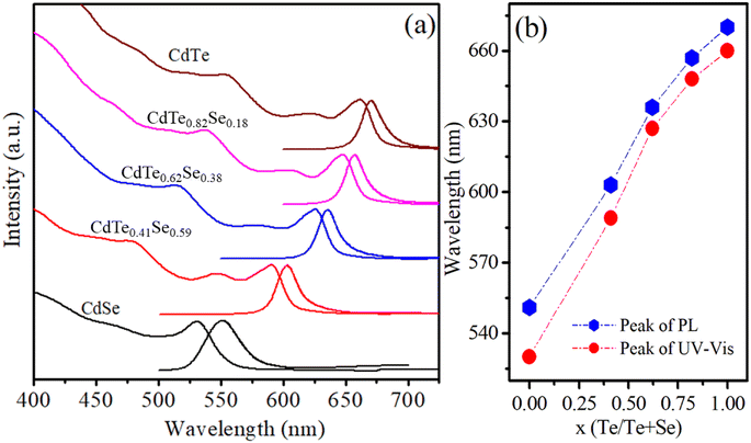 |
| | Fig. 2 (a) UV-vis absorption (Abs) and PL spectra, (b) the variation of Abs and PL peaks in relation to the composition ratio, x, of CdTexSe1−x alloy NCs. | |
Vegard's law was used to verify the uniform distribution of Se and Te in the CdTexSe1−x alloy NCs. This law represents the linear dependence of the lattice constant (a) on component x according to the following formula:26
| | |
a(CdTexSe1−x) = xa(CdTe) + (1 − x)a(CdSe)
| (1) |
where
a is the lattice constant of the CdTe, CdSe, and CdTe
xSe
1−x NCs.
x is the actual fraction of the Te element that participated in the reaction and is given in
Table 2. The
a values of the CdTe
xSe
1−x NCs are shown in
Table 2 and
Fig. 3. The results in
Fig. 3b show that the obtained values of
a from the XRD patterns and Vegard's law have large differences when
x is small. However, the bandgap energy does not depend linearly on
x, and a term is added to determine the curvature of the bandgap energy as a function of
x. This curvature correction is characterized by the
b bowing parameter:
26| | |
Eg(CdTexSe1−x) = xEg(CdTe) + (1 − x)Eg(CdSe) − bx(1 − x)
| (2) |
In the above formula,
Eg is the bandgap of the CdTe, CdSe, and CdTe
xSe
1−x NCs and is determined by the first exciton peak energy of the absorption spectrum. In this study, the values of
b were determined to be 0.154, 0.29, and 0.3 eV corresponding to the actual
x values of 0.41, 0.62, and 0.82, respectively. For CdTeSe thin-film, the
b bowing parameter is determined to be 0.75 eV.
30 The bowing parameter of
b = 0.46 eV for the Cd
1−xZn
xTe alloys.
31 The actual
x values,
a, and
Eg of the CdTe
xSe
1−x NCs were calculated and are listed in
Table 2.
Table 2 The synthetic x and actual x are determined from EDX. The lattice constants are determined from XRD and Vegard's law, and bandgap energy of CdTexSe1−x NCs
| Synthetic x |
0 |
0.3 |
0.5 |
0.7 |
1 |
| Actual x (determined from EDX) |
0 |
0.41 |
0.62 |
0.82 |
1 |
| a (determined from XRD) (Å) |
6.07 |
6.12 |
6.22 |
6.37 |
6.43 |
| a (determined from Vegard) (Å) |
6.07 |
6.21 |
6.29 |
6.36 |
6.43 |
| Bandgap energy (eV) |
2.34 |
2.11 |
1.98 |
1.91 |
1.87 |
 |
| | Fig. 3 (a) XRD patterns of CdTexSe1−x alloy NCs. (b) The dependence of the crystal lattice constant on the x ratio according to the XRD pattern and Vegard's law. The solid line is a linear fit of the data. | |
To investigate the effect of x on the structure of the CdTexSe1−x NCs, the value of x was systematically adjusted from 0 to 1. As x changed, the crystal structure of the CdTexSe1−x NCs was investigated using the XRD pattern, as depicted in Fig. 3. All the samples exhibited a ZB structure, which was confirmed by the presence of three diffraction peaks corresponding to the lattice planes (111), (220), and (311). For x = 0, the diffraction peaks observed for CdTexSe1−x NCs were consistent with the diffraction peaks positions of CdSe (PDF#19-0191), and for x = 1 consistent with the diffraction peaks positions of CdTe (PDF#15-0770).15,18 The broad diffraction peaks observed in the samples are due to the diminutive dimensions of the CdTexSe1−x NCs at the nanoscale and the strain induced in the NCs. This strain (ε) was calculated using the Stokes–Wilson equation:32
| |
 | (3) |
where
β is the full width at half maximum (FWHM) of the diffraction peak and
θ is the diffraction angle.
Dislocation density δ, that is, the total number of dislocations per unit volume of material, was determined from equation:32
| |
 | (4) |
where
D is the crystallite size of the synthesized NCs and is calculated using the Debye Scherrer formula:
33| |
 | (5) |
where,
λ = 0.154 nm, is the X-ray wavelength;
k = 0.9, and is the Scherrer constant.
The lattice constant (a) of the NC was determined from the XRD data using the following equation:
| |
 | (6) |
dhkl is the distance between the lattice planes corresponding to Miller indices
h,
k, and
l and is calculated using Bragg's equation:
32–34| | |
nλ = 2dhklsinθ
| (7) |
The position of the diffraction peaks gradually shifted towards a smaller theta angle value as x increased. This shift is due to the fact that the ionic radius of Te2− is larger than the ionic radius of Se2−. The shifting of the diffraction peaks of the CdTexSe1−x NCs indicates the formation of a homogeneous alloy structure, rather than a mere physical mixture of CdTe and CdSe NCs.
The values of a are calculated and shown in Table 3. It can be observed that when x increases from 0 to 1, a increases from 6.07 to 6.43 Å demonstrating the expansion of the unit lattice cell. The expansion of the unit lattice cell is due to the gradual substitution of smaller Se2− ions (radius: 1.96 Å) by larger Te2− ions (radius: 2.11 Å).15,35 Other reports give similar results: L. Baufay et al. indicated that the lattice constant (a) increases from 6.077 to 6.481 Å,36 while Z. Han et al. also found that (a) increases from 6.05 to 6.45 Å as the ratio of x increases from 0 to 1.29 The dependence of the lattice constant on x is shown in Fig. 3b. It can be seen that the lattice constant is linearly dependent on x, in accordance with Vegard's law, demonstrating that Te and Se ions are evenly distributed in the CdTeSe NCs. The gradual replacement of Se ions with Te ions in CdTexSe1−x NCs is believed to result in the relaxation of anion–cation bonds towards their equilibrium positions. This relaxation leads to local structural changes and a linear increase in the lattice parameters.37
Table 3 Lattice parameters and crystallite size of CdTexSe1−x alloy NCs
| Sample |
2θ (°) |
d[111] (Å) |
a (Å) |
β × 10−2 (rad) |
D (nm) |
δ × 10−2 |
ε × 10−3 |
| CdSe |
25.33 |
3.50 |
6.07 |
4.15 |
3.35 |
8.88 |
10.33 |
| CdTe0.41Se0.59 |
25.04 |
3.53 |
6.12 |
4.03 |
3.44 |
8.44 |
10.06 |
| CdTe0.62Se0.38 |
24.97 |
3.59 |
6.22 |
3.91 |
3.55 |
7.91 |
9.74 |
| CdTe0.82Se0.18 |
24.89 |
3.68 |
6.37 |
3.94 |
3.54 |
7.96 |
9.78 |
| CdTe |
24.58 |
3.71 |
6.43 |
3.96 |
3.64 |
7.56 |
9.52 |
The TEM images and particle size distributions of three typical samples: (a) CdTe, (b) CdTe0.62Se0.38, and (c) CdSe are shown in Fig. 4. The particle size distributions were calculated using ImageJ software. The TEM images showed that the obtained NCs were spherical with a narrow size distribution. The sizes of the particles were mostly in the range of 3 to 5 nm. The change in the Te/Se ratio did not significantly change the size and shape of the alloy NCs.
 |
| | Fig. 4 TEM images and particle size distributions of NCs: (a) CdTe, (b) CdTe0.62Se0.38, and (c) CdSe. | |
3.2. The influence of Gd concentration on the optical properties of CdTe1−xSex NCs
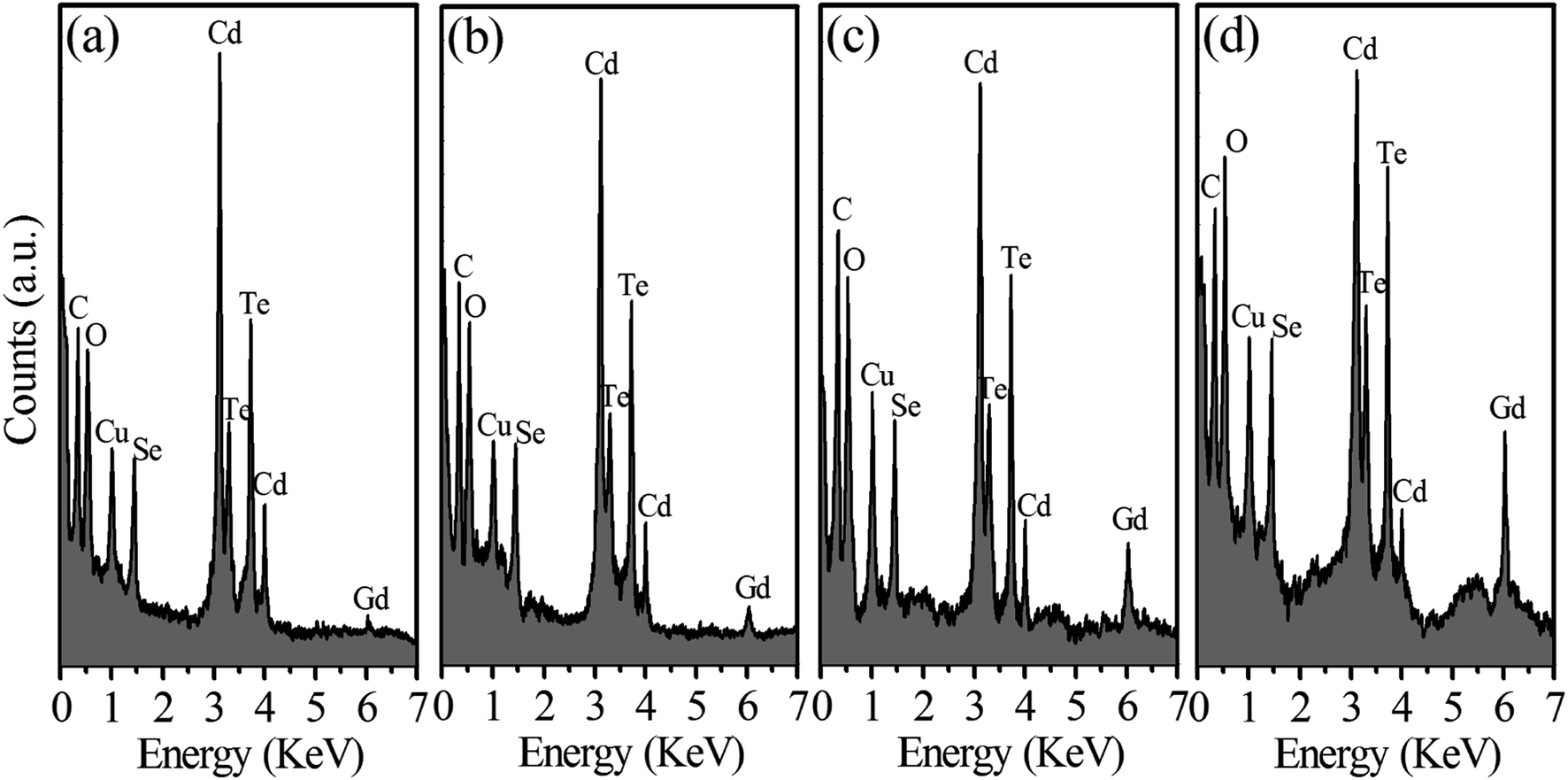
In this experiment, x = 0.5, and the impurity concentration of Gd (y) varied from 0 to 10%. EDX was used to investigate the elemental composition of the CdTe0.5Se0.5:Gd y% (y = 1–10) NCs, Fig. 5. The elemental compositions of all samples, obtained from the EDX spectra are presented in Table 4. Samples CdTe0.5Se0.5, CdTe0.5Se0.5:Gd 1%, CdTe0.5Se0.5:Gd 3%, CdTe0.5Se0.5:Gd 5%, and CdTe0.5Se0.5:Gd 10% are actually CdTe0.62Se0.38, CdTe0.64Se0.36:Gd 0.94%, CdTe0.62Se0.38:Gd 2.77%, CdTe0.60Se0.40:Gd 4.52%, and CdTe0.61Se0.39:Gd 8.05%, respectively. These samples are denoted as CTS, CTS:G1, CTS:G2, CTS:G3, and CTS:G4, respectively. Within the error limit of 5%, in this section it can be considered that x does not change but only the Gd impurity concentration changes (CdTe0.62±0.02Se0.38±0.02 denoted CdTeSe).
 |
| | Fig. 5 The EDX spectra of nanocrystals: (a) CTS:G1, (b) CTS:G2, (c) CTS:G3, and (d) CTS:G4. | |
Table 4 The composition of the atomic and weight (%) of samples
| Sample |
Atomic (%) |
Weight (%) |
| Cd |
Te |
Se |
Gd |
Cd |
Te |
Se |
Gd |
| CdTe0.5Se0.5:Gd 1% |
47.69 |
32.88 |
18.49 |
0.94 |
48.02 |
37.58 |
13.08 |
1.32 |
| CdTe0.5Se0.5:Gd 3% |
45.83 |
31.92 |
19.48 |
2.77 |
46.00 |
36.37 |
13.74 |
3.89 |
| CdTe0.5Se0.5:Gd 5% |
42.78 |
31.80 |
20.90 |
4.52 |
42.83 |
36.14 |
14.7 |
6.33 |
| CdTe0.5Se0.5:Gd 10% |
39.52 |
32.13 |
20.30 |
8.05 |
38.93 |
35.93 |
14.05 |
11.09 |
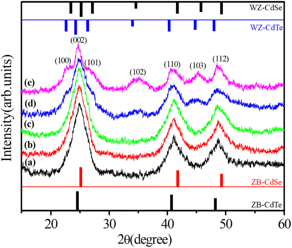
3.2.1. X-ray diffraction pattern. The structure of the host material is significantly affected by doping. Fig. 6 illustrates the effect of the Gd impurity concentration on the structure of CdTexSe1−x alloy NCs through X-ray diffraction (XRD). As the concentration of Gd (y) increased, the crystal structure of the Gd-doped CdTeSe NCs changed from zinc blende (ZB) to wurtzite (WZ). When the Gd concentration was low (0 to 2.77%), the Gd-doped CdTeSe NCs had a ZB structure. This structure is confirmed by three characteristic diffraction peaks, related to the (111), (220), and (311) planes. At a dopant concentration of 4.52%, the diffraction peaks associated with the ZB structure exhibited smearing, whereas the characteristic peaks of the WZ structure became more prominent. This result is similar to that of CdSe0.6Te0.4 alloy NCs.23 At 8.05% Gd concentration, Gd-doped CdTeSe NCs completely changed to a WZ structure with characteristic lattice planes such as (002), (102), (110), (103), and (112). This structural phase transition is closely related to the increasing degree of ionic bonding of the compounds in the Gd-doped CdTeSe alloy NCs. Gradually introducing Gd, which has an electronegativity of 1.2,29,30 into the CdTeSe NCs (including Se with an electronegativity of 3.1 and Te with an electronegativity of 2.61) leads to an increase in the ionic bonding in the CdTeSe NCs, ultimately leading to the structural phase transformation. Thus, Gd doping could serve as an important factor contributing to the transition between the two structures. An earlier theoretical study also showed a structural phase transition between ZB and WZ when Gd was doped into CdSe NCs.31
 |
| | Fig. 6 XRD pattern of NCs: (a) CTS, (b) CTS:G1, (c) CTS:G2, (d) CTS:G3, and (e) CTS:G4. | |
3.2.2. X-ray photoelectron spectroscopy. X-ray photoelectron spectroscopy (XPS) is a valuable technique for discerning the elemental composition of materials and is effective in elucidating the properties (valence) of the constituent atoms or ions by revealing their binding energies. Fig. 7a shows the typical XPS survey scans for the CdTeSe:Gd 4.52% NCs. The XPS survey scan revealed seven distinct peaks, each corresponding to different levels of Se-3d, Gd-4d, C-1s, Cd-3d, O-1s, Te-3d, and Gd-3d. Specifically, in Fig. 7b, the high-resolution XPS spectrum of Cd-3d displays two discernible peaks at 404.2 and 411.8 eV, which are indicative of the Cd 3d5/2 and Cd 3d3/2 levels of Cd2+ ions. The separation between these two peaks is 7.6 eV, which is consistent with previously reported values.38 The high-resolution XPS spectrum (Fig. 7c) of Te-3d reveals two well-defined peaks positioned at 570.8 and 581.2 eV, corresponding to the Te-3d5/2 and Te-3d3/2 levels.39 The peak observed at approximately 53.9 eV corresponds to the Se-3d level, Fig. 7d.40 The high-resolution XPS spectrum (Fig. 7e) reveals a Gd-3d spin–orbit positioned at 1186.8 eV, corresponding to the Gd-3d5/2 oxidation state.41 This result suggests that Gd ions within the CdTeSe NCs possess a +3 oxidation state.
 |
| | Fig. 7 (a) XPS survey spectrum of CdTeSe:Gd 4.52% NCs. High-resolution XPS spectra of: (b) Cd-3d, (c) Te-3d, (d) Se-3d, and (e) Gd-3d. | |
3.2.3. Absorption and photoluminescence properties. Absorption and photoluminescence spectroscopy were used to study the effect of the Gd doping on the optical properties of CdTeSe NCs. Fig. 8a shows the absorption spectra of the Gd-doped CdTeSe NCs at different Gd concentrations. The absorption spectra of the pure CdTeSe NCs have a sharp first absorption peak at 625 nm, which proves that the CdTeSe NCs have a narrow size distribution. This peak is attributed to the optical transition from the lowest energy state 1S3/2–1Se and is called the excitonic absorption peak or first absorption peak.9,15 As the Gd concentration increased, the excitonic absorption peak of the samples shifted towards a larger wavelength (red shift). This result can be attributed to two reasons: (i) Gd-doped CdTeSe NCs become larger, and/or (ii) the quantum-size effect is reduced owing to the presence of the Gd dopant incorporated into the CdTeSe NCs. The absorption peak shifted towards longer wavelengths because the binding energy of the exciton decreased with increasing size.
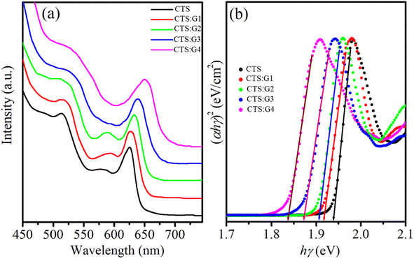 |
| | Fig. 8 (a) UV-vis spectra, and (b) the plot of variation of (αhν)2 versus (hν) of CdTeSe:Gd y% (y = 0–8.05) NCs. | |
Doping introduces defects in the crystal lattice. These defects can include vacancies, interstitial atoms, or impurities. These defects can create energy levels within the band gap, influencing the electronic structure of the material. In the case of CdTeSe, the dopant atoms used are Gd elements (the trivalent Gd3+ ions replace the position of the divalent Cd2+ ions), which create the excess of electrons in the conduction band and hence make them become to the n-type semiconductors. As a result, a new defect band (donor level) is formed below the conductor band, leading to a reduction in the bandgap of CdTeSe NCs. Similar results were also observed for Ce3+ doped ZnO and Sm3+, Tb3+ co-doped ZnS QDs.42,43
Tauc's relation was used to calculate the bandgap of the Gd-doped CdTeSe NCs.44–46
| |
 | (8) |
where
α is the absorption coefficient calculated from the equation
α = [(2.303 ×
A)/
τ] where
A is the absorbance and
τ is the path length.
hν is the energy of the excited photon, and
n is the transition coefficient, which can assume values of 1/2, 3/2, 2, and 3 for direct allowed, direct forbidden, indirect allowed, and indirect forbidden, respectively. In our case,
n = 1/2 because of the direct allowed transition of CdTeSe NCs. A graph was drawn between photon energy
hν and (
αhν)
2. The extrapolation of the linear section of the (
αhν)
2 versus (
hν) plot to the energy axis reveals a decrease in the optical bandgap energy from 1.93 eV to 1.84 eV when
y increases from 0 to 8.05% (
Fig. 8b). The effect of narrowing the bandgap energy of NCs with increasing Gd doping concentration can be due to two following reasons: (i) the local volume expansion in the CdTeSe lattice enhances interstitial defects such as Cd
i, Te
i, and Se
i, (ii) the Fermi level is lowered in the conduction band of CdTeSe and is explained by the Burstein–Moss shift.
44 The decrease in bandgap with increasing impurity concentration is also observed in material systems such as Fe-doped ZnS
45 and La-doped ZnS.
46
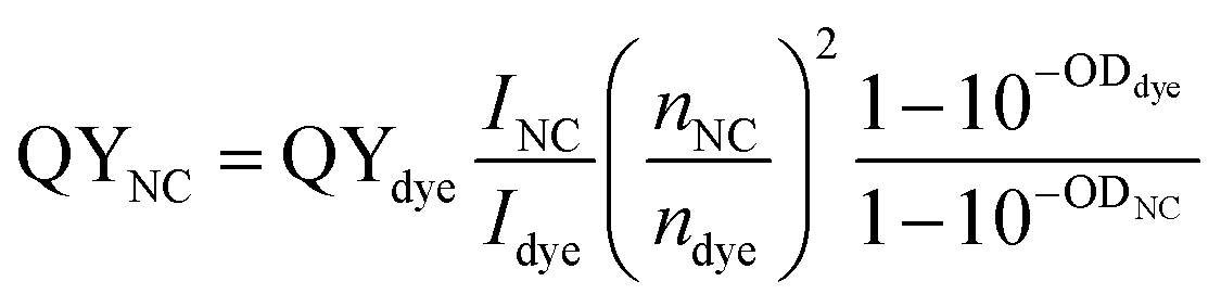
The dopant concentration significantly affected the emission characteristics of the NCs. Fig. 9 shows the photoluminescence spectra of the Gd-doped CdTeSe NCs at different Gd concentrations. The photoluminescence spectrum of pure CdTeSe NCs has an emission peak at approximately 635 nm, which is an excitonic emission arising from the recombination of electrons in the conduction band with holes in the valence band. For Gd-doped CdTeSe NCs, in addition to the excitonic emission peak, there is another emission peak at approximately 800 nm, commonly referred to as the dopant, lattice defects, and/or surface state emission. These emission types occur as electrons undergo transitions from the lower energy level of the CB of the host to localized holes situated within the dopant centers, lattice defects, and/or surface states. As the concentration of Gd increased from 0.94% to 8.05%, the doped samples exhibited a red shift in the excitonic emission (from 641 nm to 665 nm) similar to the absorption spectrum. The Gd concentration not only affects the emission wavelength of the host but also affects the quantum yield (QY) of the host and dopant. Quantum yield (QY) is a crucial parameter for assessing the emission ability of materials. The photoluminescence (PL) QY of a sample was compared to that of an organic dye with a known QY, and the calculation was performed using the following equation:15
| |
 | (9) |
where
I represents the integrated emission intensity of the PL spectrum, acquired by fitting the PL spectrum using a combination of Gaussian and Lorentzian functions.
n denotes the refractive index, and OD signifies the optical density of either the NCs or dye samples. It's worth noting that the organic dye employed in this study was Rhodamine 6G, which exhibited a QY of 95% when dissolved in ethanol. In
Fig. 9b, it is evident that as the concentration of Gd increases from 0 to 8.05%, the QY of excitonic emission decreases from 54 to 21%. This phenomenon is commonly referred to as the “PL quenching effect due to the concentration”. This effect is closely associated with non-radiative recombination processes, energy transfer mechanisms from the host to the dopant, and cross-relaxation interactions occurring among neighboring Gd
3+ ions. The results in
Fig. 9b show that when Gd concentration increases from 0 to 8.05%, the PL FWHM increases from 18–32 nm. The PL spectra of the NCs were broadened with increasing Gd concentration for three main reasons: (i) the size of the particles was not uniform, (ii) enhanced exciton scattering by lattice defects, and (iii) enhanced exciton–phonon interaction due to the lattice constant difference between Gd
3+ and Cd
2+ ions.
47,48
 |
| | Fig. 9 (a) PL spectra of CdTeSe:Gd y% (y = 0–8.05) NCs, and (b) the dependence of their QY and FWHM on Gd concentration. | |
3.2.4. Raman scattering spectrum. The Raman scattering (RS) spectrum is a powerful tool for studying mode vibrations and demonstrating the formation of alloy structures. The RS spectra of the alloyed CdTeSe:Gd y% (y = 0–8.05) NCs are shown in Fig. 10. The RS spectra of all samples have 2 peaks at 175 and 350 cm−1, corresponding to the longitudinal optical (LO) phonon peaks 1LO and 2LO of the CdTeSe alloy NCs. For CdSe and CdTe bulk semiconductors, the 1LO peaks of are located at approximately 210 and 170 cm−1, respectively.49 If separate CdTe and CdSe NCs are formed instead of CdTeSe alloy NCs, the 1LO peak of the samples appears at wave numbers less than 170 and 210 cm−1 due to the quantum confinement effect. The 1LO peaks of the CdTe and CdSe NCs were not observed. This result proves that CdTeSe NCs were fabricated successfully because their 1LO peaks are between those of CdTe and CdSe NCs. It can be seen that both the 1LO and 2LO peaks shift slightly towards smaller wave numbers as the Gd concentration increases. This shift is due to the greater replacement of large-radius Gd ions (180 pm) for small-radius Cd ions (154 pm).
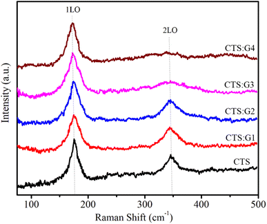 |
| | Fig. 10 Raman spectra of CdTeSe:Gd y% (y = 0–8.05) NCs. | |
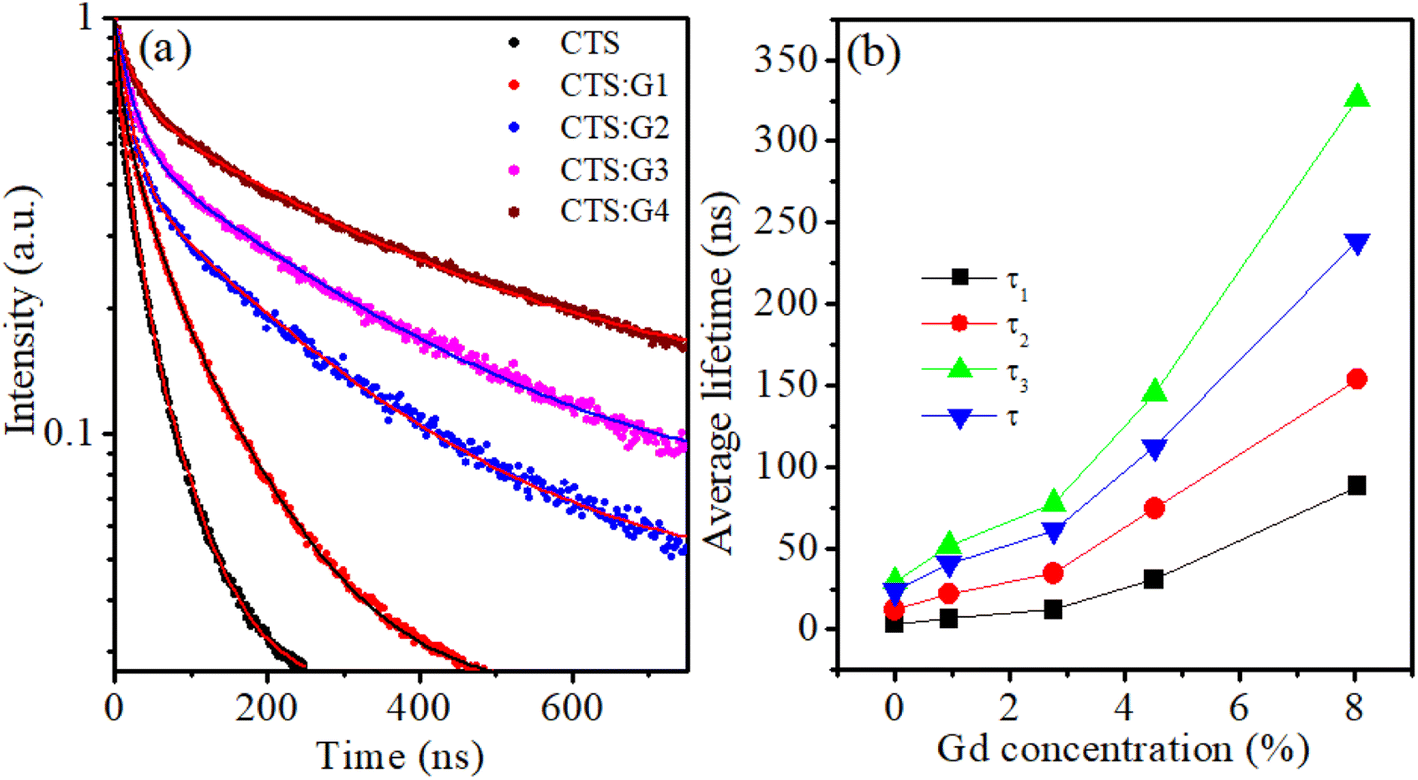
3.2.5. Photoluminescence decay curves. Emission kinetic measurement was used to study the effect of the Gd impurity concentration on the emission decay time of CdTeSe:Gd y% (y = 0–8.05) NCs. Fluorescence lifetime measurement provides useful information for investigating the emission mechanisms of a material. Fig. 11 shows the photoluminescence (PL) decay curves of the CdTeSe:Gd y% (y = 0–8.05) NCs excited at 488 nm. The observed results showed that the slope of the decay curves gradually decreased with increasing Gd concentration, indicating that a higher impurity content led to a longer PL lifetime. The decay curves for CdTeSe:Gd y% (y = 0–8.05) NCs exhibit multi-exponential behavior. The decay curves were well-fitted with the following equation:9,15,43| |
 | (10) |
where τi is the lifetime, and Ai is the pre-exponential factor. The average lifetime is determined by equation:9,15,43| |
 | (11) |
where, n = 3, is the number of components contributing to the decay processes.
 |
| | Fig. 11 (a) PL-decay kinetics of CdTeSe:Gd y% (y = 0–8.05) NCs, the solid lines present fitting curves to a multiexponential function; (b) the dependence of the lifetime values on Gd concentration. | |
The fitting constants of the time decay curves are listed in Table 5. For pure CdTeSe NCs, the constant τ1 = 3.2 ns can be ascribed to the near-band-edge emission of excitons, whereas the components τ2 = 11.8 ns and τ3 = 29.5 ns are the lifetimes of the surface-trapped charge carriers and the dark-exciton state in CdTeSe NCs, respectively.15 The average lifetime of 〈τ〉 = 23.45 ns obtained in this study, is in good agreement with the results of previous studies.15,50 The average lifetime increased from 23.45 ns to 238.98 ns (more than 10 times) when Gd concentration increased from 0% to 8.05%. The longer lifetime observed in the doped samples is the result of the existence of Gd3+ trap centers, which are positioned at greater depths than those present in the undoped sample. This reduces the overlap between the hole and electron wavefunctions that occurs because of the delocalization of these deeper states, ultimately leading to an enhanced lifetime. The significantly increased lifetimes of the Gd-doped CdTeSe NCs make them highly promising for applications in areas such as biolabeling and energy conversion.
Table 5 Experimental values of time constants obtained for CdTeSe:Gd y% (y = 0–8.05) NCs excited at 488 nm. The numbers in brackets are the amplitude percentage of each component
| Sample |
τ1 (ns) |
τ2 (ns) |
τ3 (ns) |
〈τ〉 (ns) |
| CTS |
3.2 (19.2%) |
11.8 (41.7%) |
29.5 (39.1%) |
23.45 |
| CTS:G1 |
6.5 (22.7%) |
21.7 (39.1%) |
51.3 (38.2%) |
40.56 |
| CTS:G2 |
11.8 (18.7%) |
34.3 (42.9%) |
77.4 (38.4%) |
60.7 |
| CTS:G3 |
30.7 (20.4%) |
74.2 (43.2%) |
145.1 (36.4%) |
112.3 |
| CTS:G4 |
87.8 (23.6%) |
153.3 (44.8%) |
326.4 (31.6%) |
238.98 |
3.3. The influence of Gd dopant concentration on the magnetic properties of CdTeSe NCs
Doping strongly magnetic elements such as Gd into CdTeSe semiconductor NCs significantly changes the magnetic properties of the material. The magnetic properties of powdered Gd-doped CdTeSe NCs at room temperature were studied by analyzing the magnetization, M(H), as a function of the magnetic field strength. Fig. 12 depicts the hysteresis loops of CdTeSe NCs doped with Gd, which were recorded at room temperature using a vibrating sample magnetometer. These NCs exhibited paramagnetic properties in the case of pure CdTeSe and ferromagnetic (FM) behavior with Gd-doping. Pure CdTeSe NCs exhibit paramagnetic properties, because Cd2+, Te2−, and Se2− represent nonmagnetic ions. The ferromagnetic properties of the Gd-doped CdTeSe NCs originate from Gd3+ magnetic ions and crystal lattice defects due to doping. This result demonstrates that introduction of Gd3+ ions into CdTeSe NCs can change the magnetism of the material. Table 6 presents the saturation magnetization (Ms), remanent magnetization (Mr), and (HC) coercivity values for both undoped and Gd-doped CdTeSe NCs. Notably, the saturation magnetization increased with increasing concentrations of 4f orbital dopants. No previous studies have been conducted on the magnetic properties of Gd-doped CdTeSe NCs. However, for Gd-doped ZnS nanoparticles, R. S. Kumar et al.51 previously suggested that the increase in their saturation magnetization could be attributed to the existence of sulfur vacancies, which give rise to long-range ferromagnetism. In CdTeSe NCs, the roles of Te and Se are completely similar to those of S in ZnS NCs. Therefore, as the concentration of Gd ions increased, so did the number of Te–Se vacancies. This leads to increased saturation magnetization, primarily due to ferromagnetic coupling among Gd3+ ions. As the doping concentration increased, the relationship between the magnetization and the applied magnetic field exhibited a linear trend, which is indicative of ferromagnetic behavior. The origin of this magnetism lies in the strong sp–f exchange interactions between CdTeSe and Gd3+ ions, suggesting that it is intrinsic and arises from the substitution of Gd3+ ions for Cd2+ ions. The observed room-temperature ferromagnetism is likely a result of Gd3+ substitution for Cd2+ in the CdTeSe host lattice. Increasing the concentration of Gd doping reduces the distance between Gd3+ ions and enhances the magnetization.52 Ferromagnetism in the Gd-doped CdTeSe NCs can be ascribed to the emergence of small magnetic dipoles situated on the surface of the NCs. These dipoles interact with their nearest neighbors within the NCs, leading to alignment of the dipoles in a common direction. This alignment is facilitated by the high surface-to-volume ratio of atoms in the NCs, resulting in a substantial population of magnetic dipoles oriented in the same direction, ultimately causing ferromagnetic behavior.53
 |
| | Fig. 12 M(H) data of Gd y% (y = 0–8.05) NCs at room temperature. | |
Table 6 Values of Gd-doped CdTeSe NCs magnetic properties pattern at different Gd concentrations
| Sample |
Ms (emu g−1) |
Mr (emu g−1) |
HC (kOe) |
| CTS |
0.041 |
— |
— |
| CTS:G1 |
0.153 |
0.037 |
1.01 |
| CTS:G2 |
0.23 |
0.068 |
1.22 |
| CTS:G3 |
0.289 |
0.132 |
1.89 |
| CTS:G4 |
0.376 |
0.202 |
2.39 |
However, the origin of FM in Gd-doped semiconductor NCs remains controversy.51–54 In Gd-doped CdTeSe NCs, Gd3+ ions exhibit larger magnetic moments owing to the robust FM coupling between the f-electrons of the Gd3+ ions and the s-electrons of the CdTeSe host semiconductor. As the concentration of Gd is further increased, the paramagnetic contribution becomes more pronounced owing to the presence of a large number of localized 4f electrons in the Gd ions.51,52 Unlike 3d transition metal ions, the 4f electrons of Gd are localized, necessitating indirect ferromagnetic coupling via the 5d or 6s conduction electrons. Moreover, the unique characteristics of Gd, such as its partially filled 4f and 5d orbitals, may introduce novel exchange mechanisms through intra-ion and inter-ion coupling, ultimately inducing ferromagnetism.53,54
During the doping process, Gd3+ ions substitute Cd2+ ions within the lattice, resulting in the introduction of free electrons. This incorporation of local magnetic moments through doping induces enhanced magnetic coupling and increases the Curie temperature.54 When y increased, the presence of the Gd3+ paramagnetic ions also increased, which increased the ferromagnetism of the doped sample. As shown in the inset of Fig. 12, the values of Ms have been found to be 0.041, 0.153, 0.23, 0.289, and 0.376 emu g−1 for 0, 0.94, 2.77, 4.52 and 8.05% Gd-doped CdTeSe NCs, respectively. These Ms values are similar to the Ms values obtained with Gd-doped CdS nanorods.55 An augmentation in the magnetic saturation value was observed with the introduction of Gd doping, owing to its substantial magnetic moment. This increase in saturation magnetization can be attributed to the heightened density of electron states in proximity to the Fermi level, thereby prompting ferromagnetic interactions among the Gd ions.55
4. Conclusion
CdTexSe1−x (0 ≤ x ≤ 1) and CdTeSe:Gd y% (y = 0–8.05) alloy semiconductor NCs with an average particle size of about 3–5 nm were successfully prepared using a wet chemical method. Evidence of the replacement of Cd2+ ions by Gd3+ ions was demonstrated through XRD pattern and XPS spectrum. As x increased from 0 to 1, the PL peaks of the CdTexSe1−x NCs shifted from 551 nm to 670 nm corresponding to a change in the emission color from blue to red. Doping Gd3+ ions into CdTeSe alloy NCs can simultaneously control their structures and magneto-optical properties. Notably, the crystal structure of Gd-doped CdTeSe alloy NCs changed from ZB to WZ when the Gd concentration was high above 4.52%. When Gd concentration increased from 0 to 8.05%, the QY of excitonic emission decreased from 54 to 21%, the PL lifetime of NCs increased from 23.45 to 238.98 ns, and the PL FWHM increased from 18–32 nm. These changes are caused by enhanced exciton scattering and exciton–phonon interaction by lattice defects, which are generated by the difference between Gd3+ and Cd2+ ions. The magnetic study shows that the pure CdTeSe NCs exhibit paramagnetic behavior while the Gd-doped CdTeSe NCs exhibit ferromagnetic character and the magnetization increased by three times from 0.153 to 0.376 emu g−1 upon Gd-doping. Gd-doped CdTeSe NCs with controllable optical and magnetic properties are potential materials for applications such as electronics, photonics, photocatalysts, and biosensors.
Conflicts of interest
There are no conflicts to declare.
Acknowledgements
This research was supported by Ministry of Education and Training of Vietnam under grant number B2022-TTB-03.
References
- M. Bruchez, M. Moronne, P. Gin, S. Weiss and A. P. Alivisatos, Science, 1998, 281, 2013–2016 CrossRef CAS PubMed.
- H. Peng, L. Zhang, T. H. M. Kjällman, C. Soeller and J. Travas-Sejdic, J. Am. Chem. Soc., 2007, 129, 3048–3049 CrossRef CAS PubMed.
- C. Cavallo, F. Di Pascasio, A. Latini, M. Bonomo and D. Dini, J. Nanomater., 2017, 5323164 Search PubMed.
- F. Dimroth, Phys. Status Solidi C, 2006, 3, 373–379 CrossRef CAS.
- N. Tessler, Adv. Mater., 1999, 11, 363–370 CrossRef CAS.
- S. Mirov, V. Fedorov, I. Moskalev, D. Martyshkin and C. Kim, Laser Photonics Rev., 2010, 4, 21–41 CrossRef CAS.
- V. L. Colvin, M. C. Schlamp and A. P. Alivisatos, Nature, 1994, 370, 354–357 CrossRef CAS.
- N. Tessler, V. Medvedev, M. Kazes, S. H. Kan and U. Banin, Science, 2002, 295, 506–1508 CrossRef PubMed.
- P. M. Tan, N. X. Ca, N. T. Hien, H. T. Van, P. V. Do, L. D. Thanh, V. H. Yen, V. P. Tuyen, Y. Peng and P. T. Tho, Phys. Chem. Chem. Phys., 2020, 22, 6266 RSC.
- N. T. Hien, N. X. Ca, N. T. Kien, N. T. Luyen, P. V. Do, L. D. Thanh, H. T. Van, S. Bharti, Y. Wang, N. T. M. Thuy and P. M. Tan, J. Phys. Chem. Solids, 2020, 147, 109638 CrossRef CAS.
- N. T. M. Thuy, V. T. K. Lien, P. V. Do, V. T. K. Oanh, N. X. Truong, N. X. Ca, N. T. Hien and P. M. Tan, J. Lumin., 2023, 255, 119538 CrossRef CAS.
- N. T. Hien, Y. Y. Yu, K. C. Park, N. X. Ca, T. T. K. Chi, B. T. T. Hien, L. D. Thanh, P. V. Do, P. M. Tan and P. T. T. Ha, J. Phys. Chem. Solids, 2021, 148, 109729 CrossRef CAS.
- N. X. Ca, N. D. Vinh, S. Bharti, P. M. Tan, N. T. Hien, V. X. Hoa, Y. Peng and P. V. Do, J. Alloys Compd., 2021, 883, 160764 CrossRef CAS.
- O. P. Malyk, J. Electron. Mater., 2020, 49, 3080–3088 CrossRef CAS.
- H. T. Van, N. D. Vinh, P. M. Tan, U. T. D. Thuy, N. X. Ca and N. T. Hien, Opt. Mater., 2019, 97, 109392 CrossRef CAS.
- N. X. Ca, N. D. Vinh, P. V. Do, N. T. Hien, V. X. Hoa and P. M. Tan, Phys. Chem. Chem. Phys., 2021, 23, 15257 RSC.
- N. X. Ca, H. T. Van, P. V. Do, L. D. Thanh, P. M. Tan, N. X. Truong, V. T. K. Oanh, N. T. Binh and N. T. Hien, RSC Adv., 2020, 10, 25618–25628 RSC.
- N. X. Ca, N. T. Hien, P. N. Loan, P. M. Tan, U. T. D. Thuy, T. L. Phan and Q. B. Nguyen, J. Electron. Mater., 2019, 48, 2593–2599 CrossRef CAS.
- F. J. W. Rodríguez, I. R. Chávez-Urbiola, R. Ramírez-Bon, P. Vorobiev and Y. V. Vorobiev, J. Alloys Compd., 2020, 817, 152740 CrossRef.
- P. Sheng, et al., J. Alloys Compd., 2020, 822, 153700 CrossRef CAS.
- C. Doroody, et al., Results Phys., 2023, 47, 106337 CrossRef.
- W. Xu, X. Meng, W. Ji, P. Jing, J. Zheng, X. Liu, J. Zhao and H. Li, Chem. Phys. Lett., 2012, 532, 72–76 CrossRef CAS.
- S. K. Verma, et al., Sol. Energy Mater. Sol. Cells, 2016, 157, 161–170 CrossRef CAS.
- I. F. Li and C. S. Yeh, J. Mater. Chem., 2010, 20, 2079–2081 RSC.
- H. T. Van, N. D. Vinh, N. X. Ca, N. T. Hien, N. T. Luyen, P. V. Do and N. V. Khien, Mater. Lett., 2020, 264, 127387 CrossRef CAS.
- F. Yang, P. Yang and L. Zhang, Luminescence, 2012, 28, 836–841 CrossRef PubMed.
- S. Meng and Y. Yan, J. Adv. Phys., 2016, 12, 4213–4218 CrossRef CAS.
- L. Baufay, D. Dispa, A. Pigeolet and L. D. Laude, J. Cryst. Growth, 1982, 59, 143–147 CrossRef CAS.
- Z. Han, et al., J. Alloys Compd., 2017, 699, 216–221 CrossRef CAS.
- S. Meng and Y. Yan, J. Adv. Phys., 2016, 12, 4213–4218 CrossRef CAS.
- O. Zelaya-Angel, et. al, J. Appl. Physiol., 2004, 95, 6284–6288 CrossRef CAS.
- A. K. Zak, W. H. A. Majid, M. E. Abrishami and R. Yousefi, Ceram. Int., 2011, 37, 393–398 CrossRef CAS.
- A. L. Patterson, Phys. Rev., 1939, 56, 978 CrossRef CAS.
- N. X. Ca, et al., RSC Adv., 2023, 13, 27292 RSC.
- Y. Ban and J. B. Wagner, J. Appl. Phys., 1970, 41, 2818–2823 CrossRef CAS.
- L. Baufay, D. Dispa, A. Pigeolet and L. D. Laude, J. Cryst. Growth, 1982, 59, 143–147 CrossRef CAS.
- B. Kong, T. X. Zeng, Y. G. Wu, Z. J. Fu and Z. W. Zhou, Comput. Mater. Sci., 2018, 142, 14–24 CrossRef CAS.
- Z. Yan, L. Du and D. L. Phillips, RSC Adv., 2017, 7, 55993–55999 RSC.
- C. Zeng, A. R. Ruiz, J. A. Field and R. S. Alvarez, J. Environ. Manage., 2015, 154, 78–85 CrossRef CAS PubMed.
- J. E. B. Katari, V. L. Colvin and A. P. Alivisatos, J. Phys. Chem., 1994, 98, 4109–4117 CrossRef CAS.
- S. Majeed and S. A. Shivashankar, J. Mater. Chem. B, 2014, 2, 5585–5593 RSC.
- L. F. Koao, F. B. Dejene, H. C. Swart and J. R. Botha, J. Lumin., 2013, 143, 463 CrossRef CAS.
- P. M. Tan, T. Ngoc, V. D. Nguyen, N. T. Hien, V. X. Hoa, N. X. Truong, V. T. K. Oanh, N. D. Tam, N. X. Ca, S. Bharti and Y. Peng, Opt. Mater., 2021, 114, 110901 CrossRef CAS.
- N. Suganthi and K. Pushpanathan, Surf. Rev. Lett., 2018, 25, 1850063 CrossRef CAS.
- N. Suganthi and K. Pushpanathan, J. Electron. Mater., 2018, 47, 7343–7357 CrossRef CAS.
- N. Suganthi and K. Pushpanathan, J. Mater. Sci.: Mater. Electron., 2018, 29, 13970–13983 CrossRef CAS.
- Y. Q. Chang, P. W. Wang, S. L. Ni, Y. Long and X. D. Li, J. Mater. Sci. Technol., 2012, 28, 313–316 CrossRef CAS.
- T. V. Vineeshkumar, D. R. Raj, S. Prasanth, P. Sankar, N. V. Unnikrishnan, V. P. M. Pillai and C. Sudarsanakumar, Opt. Mater., 2016, 58, 128–135 CrossRef CAS.
- P. T. Tho, N. D. Vinh, H. T. Van, P. M. Tan, V. X. Hoa, N. T. Kien, N. T. Hien, N. T. K. Van and N. X. Ca, J. Phys. Chem. Solids, 2020, 139, 109332 CrossRef CAS.
- N. T. Hien, P. M. Tan, H. T. Van, V. T. K. Lien, P. V. Do, P. N. Loan, N. T. Kien, N. T. Luyen and N. X. Ca, J. Lumin., 2020, 218, 116838 CrossRef CAS.
- R. Sanjeev Kumar, V. Veeravazhuthi, N. Muthukumarasamy, M. Thambidurai, M. Elango, A. Gnanaprakasam and G. Rajesh, SN Appl. Sci., 2019, 1, 268 CrossRef CAS.
- B. Poornaprakash, U. Chalapathi, M. Reddeppa and S. H. Park, Superlattices Microstruct., 2016, 97, 104–109 CrossRef CAS.
- K. Kaur, G. S. Lotey and N. K. Verma, J. Mater. Sci.: Mater. Electron., 2014, 25, 311–316 CrossRef CAS.
- R. S. Selinsky, J. H. Han, E. A. Morales Pérez, I. A. Guzei and S. Jin, J. Am. Chem. Soc., 2010, 132, 5997–16005 CrossRef PubMed.
- K. Kaur, G. S. Lotey and N. K. Verma, Mater. Sci. Semicond. Process., 2014, 19, 6–10 CrossRef CAS.
|
| This journal is © The Royal Society of Chemistry 2023 |
Click here to see how this site uses Cookies. View our privacy policy here. 
 Open Access Article
 This Open Access Article is licensed under a Creative Commons Attribution-Non Commercial 3.0 Unported Licence
 a,
N. T. Hien
a,
N. T. Hien