DOI:
10.1039/D3RA06162K
(Paper)
RSC Adv., 2023,
13, 29706-29720
Giant dielectric response, nonlinear characteristics, and humidity sensing properties of a novel perovskite: Na1/3Sr1/3Tb1/3Cu3Ti4O12†
Received
10th September 2023
, Accepted 4th October 2023
First published on 10th October 2023
Abstract
In this study, we unveil a novel perovskite compound, Na1/3Sr1/3Tb1/3Cu3Ti4O12, synthesized through a solid-state reaction method, exhibiting remarkable giant dielectric response, nonlinear characteristics, and humidity sensing capabilities. This research highlights the emergence of a Cu-rich phase, the properties of which undergo significant alterations depending on the sintering conditions. The optimization of sintering parameters, encompassing a temperature range of 1040–1450 °C for 1–8 h, resulted in substantial dielectric permittivity (ε′) values (∼2800–6000). The temperature dependence of ε′ demonstrated relationship to the particular sintering conditions utilized. The acquired loss tangent values were situated within encouraging values, ranging from 0.06 to 0.16 at 1 kHz. Furthermore, the material revealed distinct nonlinear electrical characteristics at 25 °C, with the nonlinear coefficient values of 5–127, depending on ceramic microstructures. Additionally, we delved deeply into the humidity-sensing properties of the Na1/3Sr1/3Tb1/3Cu3Ti4O12 material, showing a considerable variation in ε′ in response to fluctuations in relative humidity, thereby indicating its prospective application in humidity sensing technologies. The hysteresis error and response/recovery times were calculated, highlighting the versatility of this compound and its promising potential across multiple applications. The Na1/3Sr1/3Tb1/3Cu3Ti4O12 not only shows remarkable giant dielectric responses but also portrays significant promise for nonlinear and humidity sensing applications, marking it as a significant participant in the advancement of perovskite-based functional materials.
1. Introduction
Calcium copper titanate (CCTO) is a complex oxide compound that has gained significant attention in the field of materials science and engineering.1,2 One of the most notable properties of CCTO and related perovskite oxides is its exceptionally high dielectric permittivity (ε′), often reaching values in the range of 103 to 104 at room temperature.3–6 This extraordinary property is attributed to a phenomenon called the Maxwell–Wagner polarization,7,8 resulting from the accumulation of charges at the interfaces between the semiconducting grains. The existence of the internal barrier layer capacitor (IBLC) microstructure in polycrystalline CCTO ceramics has been definitively demonstrated.9–12 When subjected to an electric field, charges within the semiconducting grains of the IBLC structure can accumulate at the insulating grain boundary, leading to interfacial polarization, also commonly known as Maxwell–Wagner polarization.13 Such a high ε′ makes CCTO an ideal candidate for ceramic capacitors, where size of capacitors can be reduced without changing in capacitance value using a dielectric material with a higher ε′ value.
CCTO is composed of calcium (Ca), copper (Cu), and titanium (Ti) atoms arranged in a perovskite crystal structure. The crystal lattice structure of CCTO consists of corner-sharing octahedra formed by the arrangement of copper and titanium ions, with calcium atoms occupying the interstitial sites.14 Generally, the crystal structure of a perovskite material shows a high degree of flexibility, allowing for accommodation of a wide range of A cation sizes. However, when the octahedra tilts to create square planar sites for three quarters of the A cations like CCTO compound, the structure becomes rigid.14 Consequently, for the ACu3Ti4O12 compounds, Ca and Cd cations of A2+ size are suitable.1,14–17 Despite the strict limitation on appropriate A2+ cations for the ACu3Ti4O12 structure, numerous closely related compounds can be prepared. One method involves introducing vacancies on the A cation site, typically resulting in A3+2/3Cu3Ti4O12. Another ACu3Ti4O12 structure is the mixed monovalent (+1) and trivalent (+3) cations in A site, such as [Na+1/2Bi3+1/2] and [Na+1/2Y3+1/2].18,19
Most recently, the ACu3Ti4O12 compound was created by designing A as the mixed monovalent (+1), divalent (+2), and trivalent (+3) cations, i.e., [Na+1/3Ca2+1/3Bi3+1/3].20 The dielectric properties of this material were very attractive because a high ε′ of ∼104 with low loss tangent (tan![[thin space (1/6-em)]](https://www.rsc.org/images/entities/char_2009.gif) δ) compared to that of CCTO ceramic, which its tanδ value is usually ≫0.1. After the significantly improved giant dielectric properties of the Na1/3Ca1/3Bi1/3Cu3Ti4O12 were reported, the impressive giant dielectric properties of similar compounds were reported, such as Na1/3Cd1/3Bi1/3Cu3Ti4O12 (ref. 21) and Na1/3Ca1/3Y1/3Cu3Ti4O12.22,23 In essence, the exploration of the distinctive dielectric properties of a new dielectric material in the ACu3Ti4O12 family and its potential in capacitor applications represents a promising avenue for advancing the frontiers of electronic devices.
δ) compared to that of CCTO ceramic, which its tanδ value is usually ≫0.1. After the significantly improved giant dielectric properties of the Na1/3Ca1/3Bi1/3Cu3Ti4O12 were reported, the impressive giant dielectric properties of similar compounds were reported, such as Na1/3Cd1/3Bi1/3Cu3Ti4O12 (ref. 21) and Na1/3Ca1/3Y1/3Cu3Ti4O12.22,23 In essence, the exploration of the distinctive dielectric properties of a new dielectric material in the ACu3Ti4O12 family and its potential in capacitor applications represents a promising avenue for advancing the frontiers of electronic devices.
Besides the capacitor applications, there have been reports about the potential application of CCTO ceramics as humidity sensors.24–26 Humidity sensing plays a pivotal role in numerous applications spanning industries such as environmental monitoring, agriculture, food production, and industrial processes.27 Capacitive humidity sensors, in particular, have gained significant attention due to their sensitivity, reliability, and ease of integration.25,28,29 Furthermore, capacitive-type sensors are particularly promising due to their simple capacitor structure, which facilitates miniaturization, and cost-effectiveness. Importantly, capacitance can be effortlessly amplified using oscillator circuits.24,25,30 These sensors operate on the principle that the ε′ (or capacitance) of a material changes in response to variations in humidity, leading to changes in capacitance. As a result, capacitive humidity sensors offer a versatile and efficient means of quantifying moisture levels in various environments. To optimize the performance of capacitive humidity sensors, the choice of sensing materials is of paramount importance. Researchers have extensively explored a diverse range of dielectric materials.24–26,28,29
While elements such as Bi1/3 and Y1/3, as well as other lanthanide ions, have been extensively researched in ACu3Ti4O12 compounds,21–23 the incorporation of Tb remains less explored. Previous studies have demonstrated that doping CCTO ceramics with Tb can significantly improve their nonlinear electrical properties.31 Additionally, the mixed valence states of Tb3+/Tb4+ might offer electrical compensation in instances of Na evaporation.32 In this work, we represented the synthesis and analytical exploration of a novel perovskite compound, Na1/3Sr1/3Tb1/3Cu3Ti4O12. Characterized by an interesting giant dielectric response, nonlinear characteristics, and potent humidity-sensing capabilities, this material showed notable advancements in the field of perovskite-based functional materials. The investigation not only uncovers the substantial ε′ values attained through optimized sintering conditions but also highlights the promising potential of this compound in nonlinear and humidity sensing applications.
2. Experimental details
A wet-ball milling technique was employed to prepare Na1/3Sr1/3Tb1/3Cu3Ti4O12, [NST]CTO, powders. The starting materials used were Na2CO3 (99%), SrCO3 (99.9%), Tb4O7 (99.95%), CuO (99%), and TiO2 (99.9%). Initially, a wet-ball milling process was conducted to mix the powders of the starting materials in ethanol, utilizing ZrO2 balls with a diameter of 2 mm. Subsequently, the ZrO2 balls were separated, and the ethanol was evaporated in an oven at 80 °C for 24 h. Thereafter, the mixed powders were ground using a mortar and pestle and calcined at 950 °C for 5 h at a heating rate of 5 °C min−1, followed by natural cooling to room temperature. Following this, the calcined powder was ground again and pressed into pellets to create the green body, using a uniaxial compressive stress of 200 MPa, omitting the use of a polymeric binder. The pellets had a diameter of 9.5 mm and a thickness of 1.2 mm. In the final stage, the green bodies were sintered at temperatures of 1020, 1030, 1040, and 1050 °C for a duration of 4 h to investigate the effect of sintering temperature (Ts). Additionally, some green bodies were sintered at 1050 °C for periods of 1 and 2 h, and at 1040 °C for 8 h to investigate the effect of sintering time (ts). It should be noted that the samples began to melt when sintered at 1060 °C. The notation for the sintered ceramics is based on a specific pattern: the Ts (in °C) followed by the ts (in hours), formatted as 10X0/Y. For example, a sample sintered at a temperature of 1020 °C for a duration of 2 h would be denoted as the 1020/2 sample. It is important to note that all heat treatments were performed in the atmosphere.
Initially, we measured the densities of all sintered ceramics using the Archimedes method. We then calculated the relative densities (ρr). The calcined powder and sintered ceramics were characterized using X-ray diffraction (XRD) with a PANalytical EMPYREAN instrument, complemented by field-emission scanning electron microscopy (FE-SEM; accelerating voltage of 20 kV) and energy-dispersive X-ray analysis (EDS) conducted on a HITACHI SU8030 instrument from Japan. The XRD spectra were acquired over a 2θ range of 20° to 80°, with a step size of 0.02° and a dwell time of 30 seconds per step. We employed the continuous/scanning (θ − 2θ) mode. The equipment operated at 45 kV and 40 mA, utilizing CuKα radiation with a wavelength (λ) of 0.15406 nm. Additionally, the SEM-mapping technique was utilized to systematically analyze the sintered specimens. The mean grain size of the sintered samples, along with the average particle size and size distribution of the powder, were determined from the SEM images. We determine grain size by measuring the circumference of each grain using Adobe software. The grain size is then defined as the diameter of a circle whose circumference matches that of the grain. The average grain size is derived from an assessment of ∼200 grains.
The dielectric properties and nonlinear current density–electric field (J–E) characteristics were evaluated. Air-dried silver (Ag) paint was used as the electrode material and was applied to both sides of the polished samples to form a simple parallel plate capacitor. Dielectric parameters were evaluated utilizing a KEYSIGHT E4990A Impedance Analyzer, spanning a frequency range of 40 Hz to 107 Hz, employing an oscillating voltage with an amplitude of 0.5 V. Measurements were conducted over a temperature range of −100 to 150 °C in an atmospheric environmental humidity–temperature chamber (ESPEC SH-222 model). To investigate the humidity-sensing properties, dielectric parameters were measured at 25 °C, with frequencies between 40 and 106 Hz, across various levels of relative humidity (RH) ranging from 30% to 90% RH, utilizing the aforementioned chamber. Subsequently, the response–recovery times, repeatability, and hysteresis error were calculated.
For varistor application, the nonlinear electrical characteristics were assessed using a high-voltage unit, specifically the Keithley Model 247. The setup was immersed in silicone oil to prevent flashover-induced breakdown between the top and bottom electrodes. The DC voltage (V) range was applied from 0 to 2000 V. The current (I) was measured. The sweep rate for the nonlinear tests was 0.95 V s−1. The α value was computed using the following formula:
| |
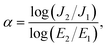 | (1) |
where
E1 and
E2 are the electric fields, at which
J1 = 1 and
J2 = 10 mA cm
−2, respectively. The breakdown electric field (
Eb) was defined as equal to being
E1. Note that
J and
E were determined using the relations
J =
I/
A and
E =
V/
d, where
A and
d were the electrode area (0.61 cm
2 for all samples) and the thickness of the sintered sample, respectively. The geometric factors
A/
d were taken into account for all impedance data, allowing for a comparison of the contributions of various regions to the overall response.
33
3. Results and discussion
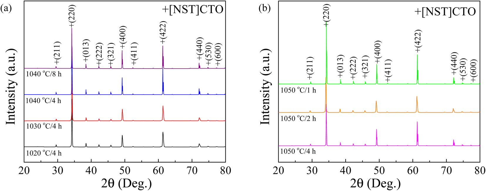
Firstly, the phase composition and crystal structure of the sintered [NST]CTO ceramics were examined to verify the successful synthesis of the designed material. As depicted in Fig. 1, the dominant phase, resembling the CCTO-like compound with a body-centered cubic perovskite structure with a space group Im![[3 with combining macron]](https://www.rsc.org/images/entities/char_0033_0304.gif) (75-2188), is observed in the XRD patterns of all ceramics without additional diffraction peaks. The overall XRD patterns closely align with the known CCTO compound,4,8,25 allowing these diffraction peaks to be indexed as the [NST]CTO phase, which shares the same crystal structure, as observed in the CCTO compound. However, the existence of a secondary phase, undetectable by the XRD technique due to instrument resolution limitations, cannot be ruled out. Various CCTO-like compounds have been fabricated and reported in the literature, including Na1/3Ca1/3Bi1/3Cu3Ti4O12,20 Na1/3Cd1/3Bi1/3Cu3Ti4O12,21 and Na1/3Ca1/3Y1/3Cu3Ti4O12,22 with lattice parameters (a = b = c) of 7.400, 7.408, and 7.387 Å, respectively. The a value of CCTO is 7.391 Å.14 Consequently, further crystal characterization was undertaken using the Rietveld refinement technique, as demonstrated in Fig. S1 and S2 (ESI†). The associated fitting parameters and cell parameters have been summarized in Table 1. The a values of the [NST]CTO sintered under different conditions ranged from 7.399 to 7.402 Å, fluctuating slightly by approximately 0.04% with changes in Ts. The bond lengths slightly vary compared to the perovskite structure of the CCTO compound. Hence, a novel perovskite with a body-centered cubic structure with an Im space group, denoted as [NST]CTO, can be fabricated.
(75-2188), is observed in the XRD patterns of all ceramics without additional diffraction peaks. The overall XRD patterns closely align with the known CCTO compound,4,8,25 allowing these diffraction peaks to be indexed as the [NST]CTO phase, which shares the same crystal structure, as observed in the CCTO compound. However, the existence of a secondary phase, undetectable by the XRD technique due to instrument resolution limitations, cannot be ruled out. Various CCTO-like compounds have been fabricated and reported in the literature, including Na1/3Ca1/3Bi1/3Cu3Ti4O12,20 Na1/3Cd1/3Bi1/3Cu3Ti4O12,21 and Na1/3Ca1/3Y1/3Cu3Ti4O12,22 with lattice parameters (a = b = c) of 7.400, 7.408, and 7.387 Å, respectively. The a value of CCTO is 7.391 Å.14 Consequently, further crystal characterization was undertaken using the Rietveld refinement technique, as demonstrated in Fig. S1 and S2 (ESI†). The associated fitting parameters and cell parameters have been summarized in Table 1. The a values of the [NST]CTO sintered under different conditions ranged from 7.399 to 7.402 Å, fluctuating slightly by approximately 0.04% with changes in Ts. The bond lengths slightly vary compared to the perovskite structure of the CCTO compound. Hence, a novel perovskite with a body-centered cubic structure with an Im space group, denoted as [NST]CTO, can be fabricated.
 |
| | Fig. 1 (a) XRD patterns of [NST]CTO ceramics sintered at 1020, 1030, and 1040 °C for 4 h and 1040 °C for 8 h. (b) XRD patterns of [NST]CTO ceramics sintered at 1050 °C for 1, 2, and 4 h. | |
Table 1 Structural parameters obtained through Rietveld refinement and relative density (ρr) of [NST]CTO ceramics sintered at different conditions
| Sample (sintering condition) |
1020/4 |
1030/4 |
1040/4 |
1040/8 |
1050/4 |
1050/2 |
1050/1 |
| a (Å) |
7.399 |
7.399 |
7.402 |
7.400 |
7.398 |
7.402 |
7.396 |
| Rexp (%) |
5.746 |
5.783 |
5.675 |
5.805 |
5.595 |
7.402 |
5.909 |
| Rp (%) |
7.715 |
4.627 |
5.591 |
8.133 |
4.628 |
5.476 |
5.315 |
| GOF |
2.877 |
1.368 |
2.061 |
2.942 |
1.544 |
1.988 |
1.657 |
|
| Bond length (Å) A = Cu and B = Ti |
| A–O |
1.976 |
1.976 |
1.976 |
1.976 |
1.975 |
1.976 |
1.975 |
| B–O |
1.960 |
1.960 |
1.961 |
1.961 |
1.960 |
1.961 |
1.960 |
| B–A |
3.204 |
3.204 |
3.205 |
3.204 |
3.203 |
3.205 |
3.203 |
| B–Ca |
3.204 |
3.204 |
3.205 |
3.204 |
3.203 |
3.205 |
3.203 |
| ρr (%) |
65.3 |
67.3 |
98.7 |
99.9 |
96.1 |
89.5 |
86.4 |
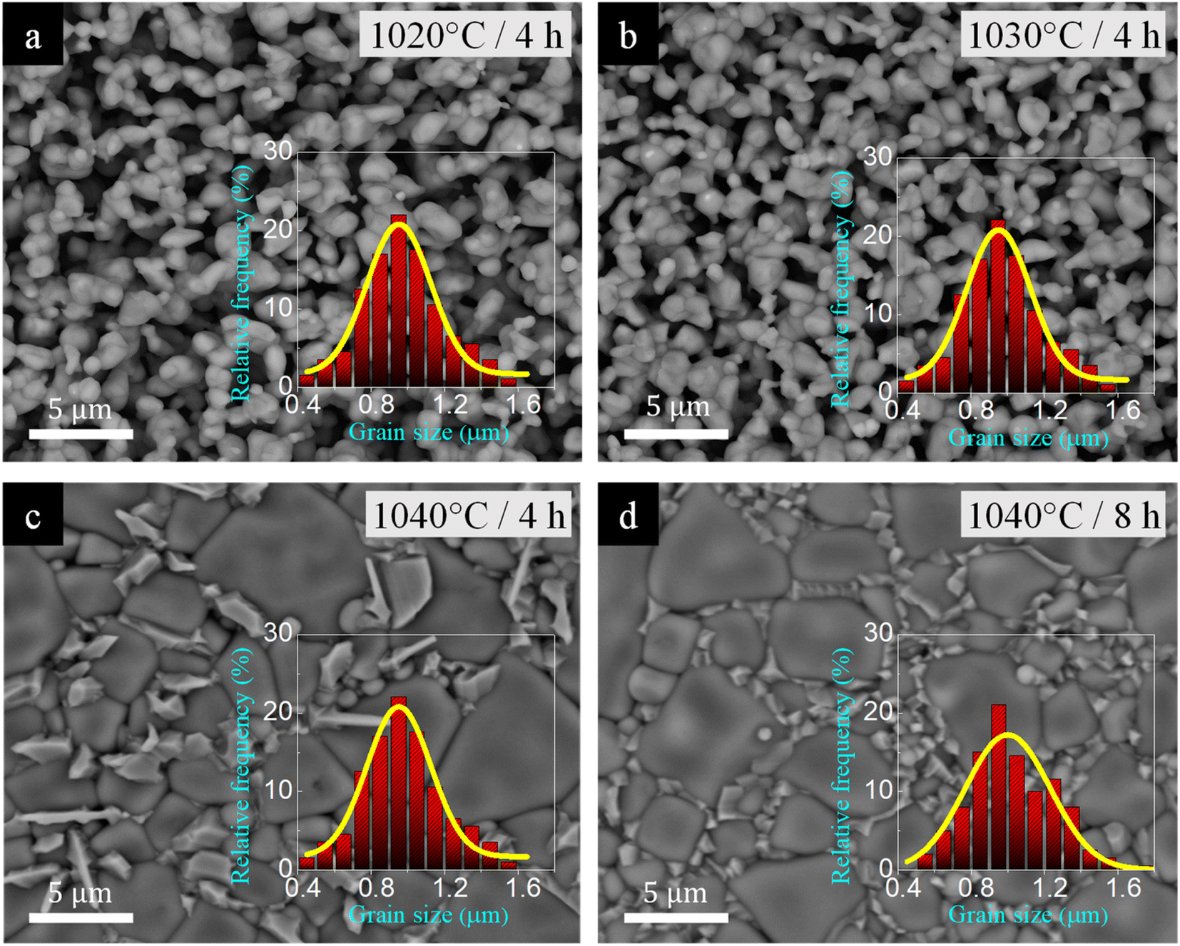
As is well known, the dielectric properties of the ACu3Ti4O12 family are closely related to the microstructure, which can typically be modified by adjusting Ts and ts.3,11 Consequently, the influence of sintering conditions on the microstructural evolution of [NST]CTO was characterized. First of all, the ρr values for all sintered ceramics were listed in Table 1. As illustrated in Fig. 2(a) and (b), both the 1020/4 and 1030/4 samples contain a significant amount of pores and exhibit nearly identical average grain sizes and narrow grain size distributions. This corresponds to their low ρr values of 65.3% and 67.3%, respectively. Notably, the microstructure underwent a dramatic change when the Ts was raised from 1030 to 1040 °C for 4 h, resulting in a ρr of 98.7%, as depicted in Fig. 2(c). The 1040/4 sample revealed a dense ceramic composition, characterized by regular, smooth surface grains and a presence of rock-like grains; the latter are commonly identified as the CuO/Cu2O secondary phase.34 The rapid escalation in grain size observed in CCTO and analogous compounds is widely attributed to the liquid phase sintering mechanism.11,35,36 As seen in Fig. 2(d), when the ts extended to 8 h (in the 1040/8 sample), the regular grains exhibited a slight enlargement with a high ρr of 99.9%. Simultaneously, the anticipated CuO/Cu2O phase particles in the 1040/8 sample diminished in size and dispersed homogeneously along the grain boundaries.
 |
| | Fig. 2 Surface morphologies of [NST]CTO sintered at (a) 1020 °C for 4 h, (b) 1030 °C for 4 h, (c) 1040 °C for 4 h, and (d) 1040 °C for 8 h; insets display grain size distribution. | |
To further substantiate this assumption, the SEM-EDX mapping technique was employed. Fig. 3(a) and (b) depict the elemental mapping images of the 1040/4 and 1040/8 samples, respectively. Notably, the rock-like grains in Fig. 3(a) are confirmed to be CuO/Cu2O phases, which are dispersed quite homogeneously along the grain boundaries when the ts increased to 8 h (1040/8 sample, Fig. 3(b)). As depicted in Fig. S3 within the ESI,† the EDS spectra, as acquired from various grains, substantiate the presence of the CuO/Cu2O phase.
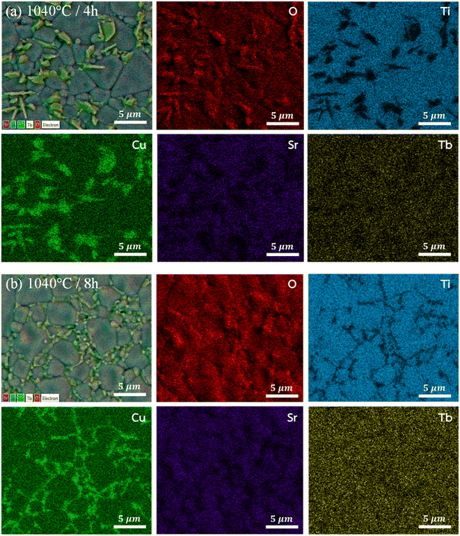 |
| | Fig. 3 SEM-mapping images for elements of [NST]CTO sintered at (a) 1040 °C for 4 h and (b) 1040 °C for 8 h. | |
In Fig. 4(a), we noted a similar trend in microstructural evolution between the 1040/4 and 1050/4 samples, as well as between the 1040/4 and 1040/8 samples. In both cases, the [NST]CTO grains notably enlarged, accompanied by a more uniform dispersion of CuO/Cu2O along the grain boundaries as the Ts and ts increased. Upon examining the microstructural evolution of the 1050/4, 1050/2, and 1050/1 samples, as depicted in Fig. 4(a)–(c), we observed continuous changes in the microstructure with ρr values of 96.1, 89.5, and 86.4%, respectively. Particularly, the microstructure of the 1050/1 sample, especially in terms of the segregation of the CuO/Cu2O phase, bore a strong resemblance to that of the 1040/4 sample. The SEM mapping images presented in Fig. S4(a) and (b)† affirm the similarities in the overall microstructure between the 1040/4 and 1050/1 samples, as well as between the 1040/8 and 1050/4 samples. Fig. 4(d) reveals the morphologies of [NST]CTO powder. It is crucial to note that the segregation of the CuO/Cu2O phase occurred in the sintered ceramics, even when the impurity phase is undetectable in the XRD pattern of the [NST]CTO powder, calcined at 900 °C for 5 h, as shown in Fig. S5.†
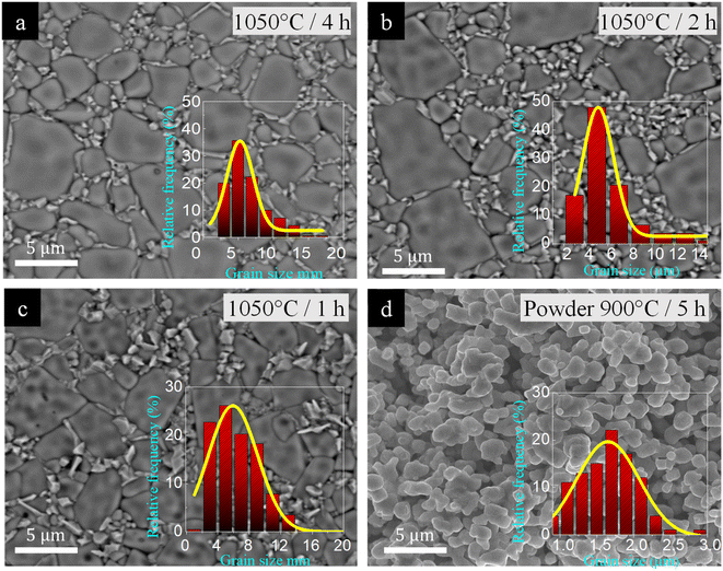 |
| | Fig. 4 Surface morphologies of [NST]CTO sintered at (a) 1050 °C for 4 h, (b) 1050 °C for 2 h, (c) 1050 °C for 1 h, and (d) [NST]CTO powder calcined at 900 °C for 5 h; insets display grain size and particle size distribution. | |
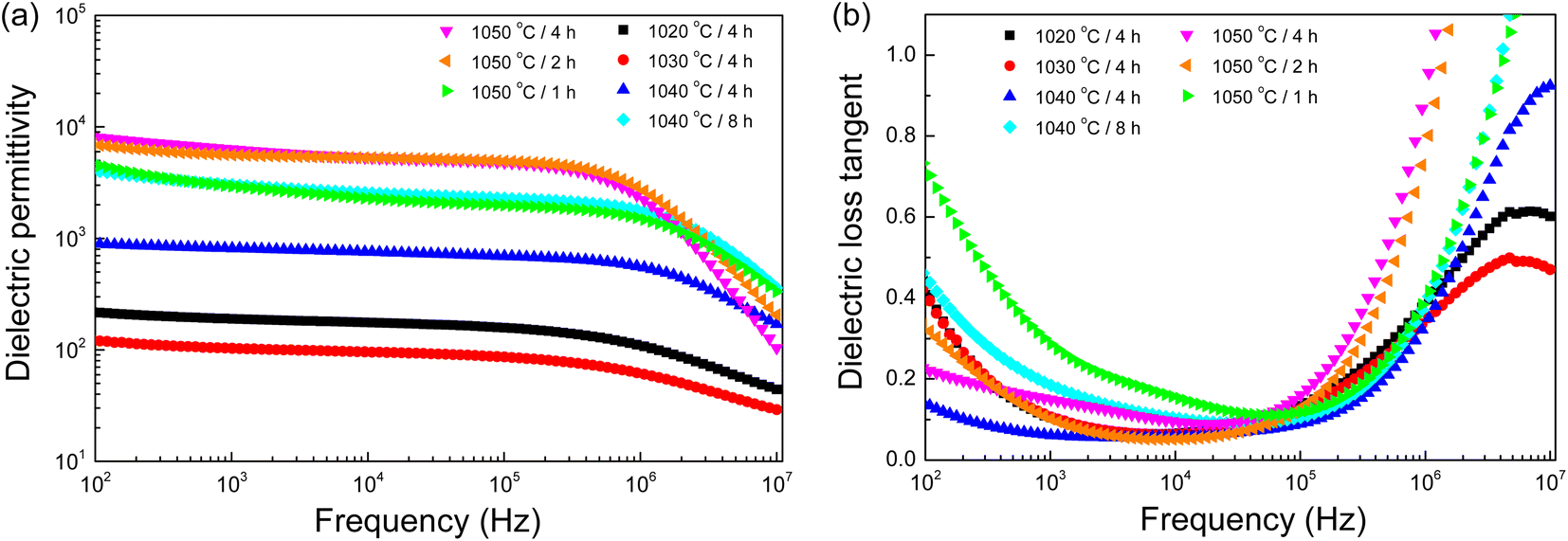
We investigated the frequency-dependent dielectric response of distinct samples, each subjected to different sintering conditions. As illustrated in Fig. 5(a), the ε′ values of all samples maintain a near-static state across a wide frequency range, spanning from 103 to 106 Hz, thereby indicating a frequency independence within this region. However, a notable deviation becomes evident as the frequency surpasses 106 Hz, where the ε′ values exhibit a marked decrease, a phenomenon attributed to the activation of the dielectric relaxation mechanism.7,8,18 Further, a critical examination of the influence of sintering conditions on the ε′ unveils a discernible pattern. The ε′ values at 1 kHz and 20 °C are listed in Table 2. The 1020/4, 1030/4, and 1040/4 samples exhibited ε′ values that remained below the threshold of 103 across the investigated frequency spectrum. This value is significantly lower compared to their counterparts. As depicted in the SEM images, the low ε′ values of the 1020/4 and 1030/4 samples (∼200) can be primarily attributed to their porous microstructures. The denser 1040/4 sample exhibited a higher ε′ of ∼550, which may be ascribed to a reduced capacitance at grain boundaries.11 On the other hand, the remaining samples, characterized by a dense ceramic microstructure, manifested a notable escalation in ε′ values, breaching the 103 threshold and hence delineating a giant ε′ behavior—a significant achievement in the context of novel perovskite [NST]CTO ceramics. Special recognition is warranted for the 1050/2 and 1050/4 samples, which exhibited exceptional performance, registering astonishing ε′ values of ∼5500 and 5800, respectively. This groundbreaking development in the study of perovskite ceramics underscores the vital role that sintering conditions play in modulating the ε′ values.
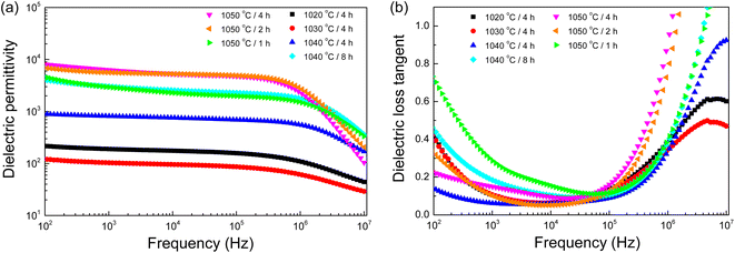 |
| | Fig. 5 (a) Dielectric permittivity (ε′) and (b) loss tangent (tanδ) at 25 °C (102–107 Hz) for all sintered ceramics. | |
Table 2 Dielectric properties (ε′ and tanδ), nonlinear J–E parameters (α and Eb), and humidity sensing parameter (γH) of [NST]CTO ceramics sintered at different conditions
| Sample |
Dielectric properties 1 kHz |
Nonlinear properties |
Humidity sensing property |
| E′ (20 °C) |
tanδ (20 °C) |
Eb (V cm−1) |
α |
γH (%) |
| 1020/4 |
218 |
0.33 |
16687 |
127 |
— |
| 1030/4 |
218 |
0.28 |
13649 |
45 |
— |
| 1040/4 |
544 |
0.06 |
1634 |
7 |
— |
| 1040/8 |
2725 |
0.14 |
1292 |
11 |
— |
| 1050/4 |
5838 |
0.10 |
2305 |
6 |
10 |
| 1050/2 |
5479 |
0.06 |
985 |
5 |
17 |
| 1050/1 |
2679 |
0.16 |
1534 |
7 |
11 |
Fig. 5(b), we analyze the behavior of the tanδ across a broad frequency range of 102 to 107 Hz at 20 °C for all samples. At high frequency ranges, a rapid increment in the tanδ was observed, which corresponded to a decrease in the ε′, thereby affirming the occurrence of dielectric relaxation phenomena.7,8 Conversely, in the low-frequency range, a substantial increase in the tanδ was witnessed, largely attributable to the long-range movement of free charges near the electrode, a phenomenon referred to as DC conduction.37,38 Particularly, the 1050/2 and 1050/4 samples demonstrated low tanδ values at 1 kHz, indicative of their superior performance within this study. Table 2, these values, recorded at 1 kHz and 20 °C, were the lowest among all the tested samples, which also exhibited the highest ε′.
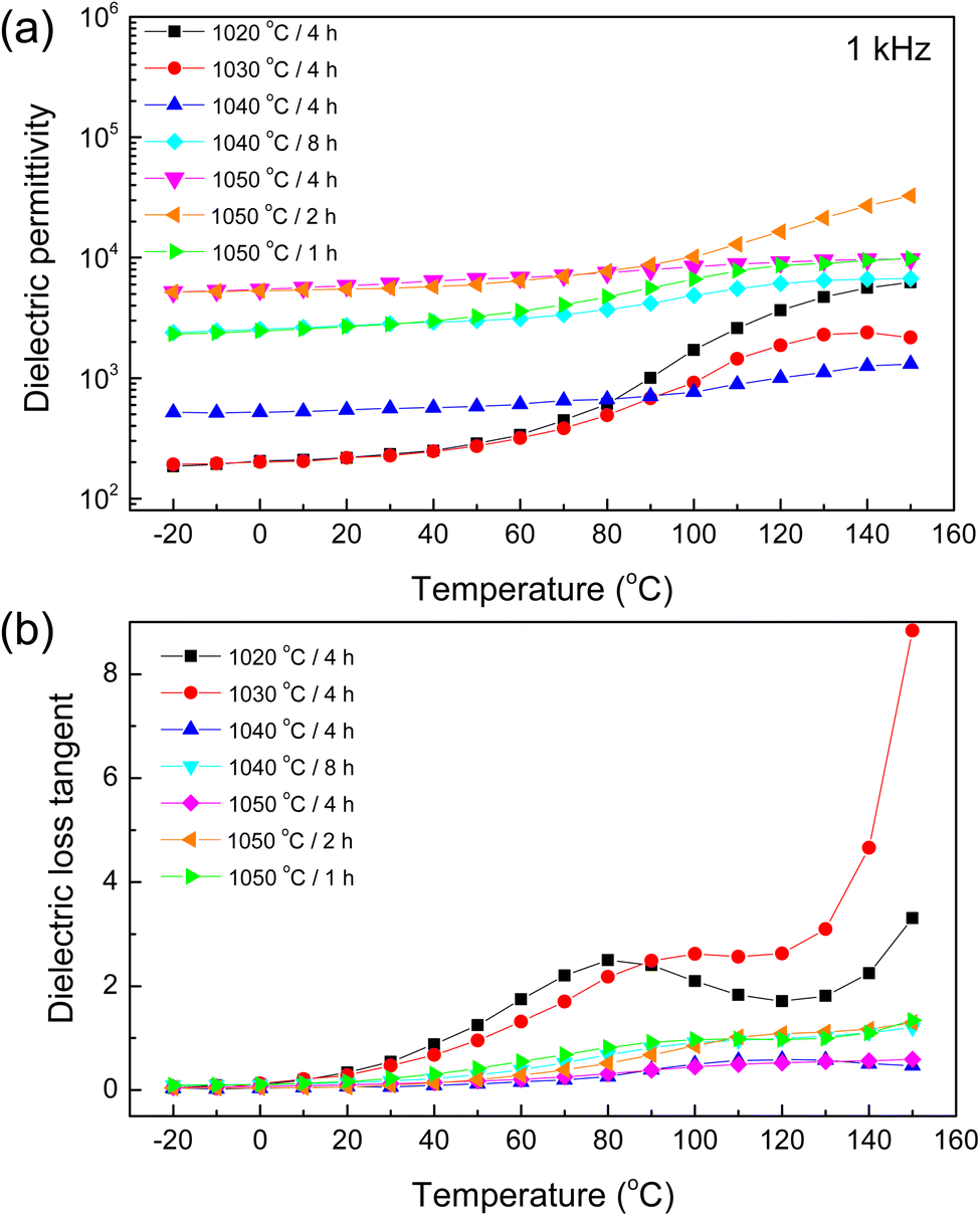
As depicted in Fig. 6(a), initial observations highlighted a marked variation in the ε′, particularly at temperatures exceeding 60 °C. This analysis delineated a distinctive pattern emphasizing the robust temperature dependency of the ε′ across most samples, with the notable exception of the 1050/4 sample. This specimen exhibited remarkable stability in its ε′ throughout the entire temperature span investigated, indicating an inherent resilience to temperature-induced fluctuations. In contrast, the 1020/4 and 1030/4 samples experienced substantial variations in their ε′ values, particularly beyond the 60 °C benchmark, hinting at a potential variation in material polarization mechanisms at higher temperature regimes.39 Fig. 6(b), the tanδ analysis portrayed a trend of ascending values concomitant with rising temperatures, particularly prominent in the higher temperature. This pronounced increase in tanδ primarily resulted from a heightened DC conduction phenomenon.8,37,39 Remarkably, the 1050/4 sample distinguished itself, not only demonstrating a diminished tanδ but also exhibiting significant stability across varying temperature conditions. This behavior hints at the potentiality that the sintering conditions adopted for this sample facilitated a microstructural configuration that is inherently favorable, leading to enhanced stability and reduced energy loss characteristics.
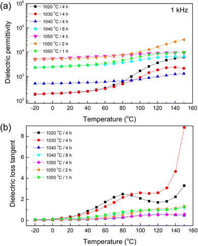 |
| | Fig. 6 (a) Dielectric permittivity (ε′) and (b) loss tangent (tanδ) at 1 kHz (−20–150 °C) for all sintered ceramics. | |
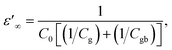
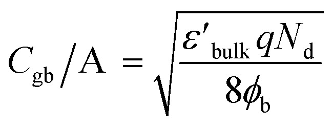
According to the internal barrier layer capacitor (IBLC) theory and impedance spectroscopy,7,11 the significant dielectric response in CCTO-based materials is closely associated with the insulating grain boundaries and the electrical characteristics of the semiconducting grains.3,9–12 In this setting, the insulating grain boundaries predominantly influence the tanδ behavior. The grain resistance (Rg) can be deduced from the nonzero intercept on the Z′-axis,10–12 close to the origin at high frequencies. Specifically, in the case of CCTO ceramics, which are capable of exhibiting ε′ values approximately equal to 104, the Rg was found to be below 100 Ω cm around room temperatures.8,11 Notably, as delineated in Fig. 7(a), the ceramics denoted as 1020/4, 1030/4, and 1040/4 – which fail to exhibit a giant dielectric response (ε′ < 103) – presented considerably high Rg values at 20 °C. This Rg exhibited a decreasing trend, falling from 2.2 to 1.0 kΩ cm with an increase in Ts from 1020 to 1040 °C. This trend suggests an increase in the number of internal free electrons (Nd), and consequently, a rise in the ε′ values, as is illustrated by the following equation:12,40
| |
 | (2) |
where
Cgb/A represents the grain boundary capacitance per unit area,

is the permittivity of bulk material, and
ϕb is the potential barrier height at the grain boundary. On the other hand, as shown in
Fig. 7(b), a surge in
Ts to 1050 °C led to a substantial reduction in
Rg, ranging between 0.2 and 0.4 kΩ cm. This shift resulted in further enhanced
ε′ values for the 1050/2 and 1050/4 specimens, exceeding the 1040/5 sample. Adams
et al.9 observed that, around room temperature, a CCTO ceramics
Z* plot displayed only a nonzero intercept without any evident semicircular arc in the lower MHz region. They attributed this behavior to the electrical response of the semiconducting grains. Later, Sinclair
et al.,
10 conclusively demonstrated that a semicircular arc become visible at temperatures around −100 °C. This observation aligned with what was seen in the [NST]CTO ceramics, as highlighted in the inset of
Fig. 7(b).
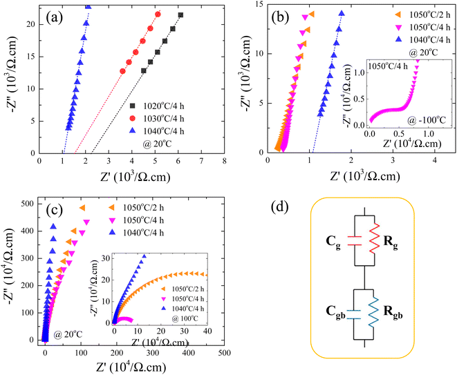 |
| | Fig. 7 (a) Z* plots at 20 °C for [NST]CTO sintered at 1020, 1030, and 1040 °C for 4 h near the origin for showing a nonzero intercept on Z′-axis. (b and c) Z* plots at 20 °C of [NST]CTO sintered at 1050 °C for 2 and 4 h compared to that sintered at 1040 °C for 4 h for showing a nonzero intercept on Z′-axis and for revealing overall spectra, respectively; inset displays Z* plots at 100 °C for showing large semicircular arcs for the insulating grain boundary response. (d) Equivalent circuit for IBLC microstructure of [NST]CTO polycrystalline ceramic. | |
As depicted in Fig. 7(c) and its inset, prominent semicircular arcs are evident, symbolizing the reactions at the insulating grain boundaries.3,7,11 Clearly, the dielectric properties of the [NST]CTO ceramics are influenced by the IBLC effect. This relationship forms the basis for the correlation between the ε′ and Rg values, employed to articulate the dielectric responses observed in the [NST]CTO ceramics, following the IBLC model. When subjected to an external electric field, there is a heightened movement of free charges within the semiconducting grains towards the grain boundary interface, resulting in intensified interfacial polarization and consequently, higher ε′ values, particularly for the 1050/2 and 1050/4 samples. It is noteworthy that in the [NST]CTO ceramics, the semicircular arcs representing the grains and grain boundaries exhibit relatively low and high resistances, respectively. As a result, the microstructure can be characterized as having an IBLC configuration. The ideal equivalent circuit for this microstructure comprises two parallel RC elements connected in series: one RC element for the bulk and another for the grain boundary response.7,11,12 This circuit is illustrated in Fig. 7(d).
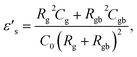
Based on the IBLC microstructure, the primary cause of a large ε′ value is likely the interfacial polarization, also known as Maxwell–Wagner polarization.13 To delve deeper into the origins of the substantial dielectric properties, we employed the modified Maxwell–Wagner relaxation model based on the equivalent circuit (Fig. 7(d)) for IBLC microstructure to fit the experimental data. Accordingly, Z* can be expressed as:7
| |
 | (3) |
where
Z′ and
Z′ represent the real and imaginary parts of
Z*, respectively.
Rg and
Rgb are the grain and grain boundary resistance values, respectively, while
Cg and
Cgb represent the grain and grain boundary capacitance values. The dielectric complex dielectric permittivity (
ε*) can be derived as,
| |
 | (4) |
where
ε′ and
ε′′ =
ε′
tan
δ represent the real and imaginary parts of
ε*, respectively.

and

denote the dielectric permittivities at low and high frequency respectively.
τ is a relaxation time. The last term reflects the impact of conductivity on energy loss.
| |
 | (5) |
| |
 | (6) |
| |
 | (7) |
| |
 | (8) |
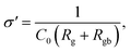
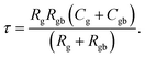
Experimental results of [NST]CTO (Fig. 7) showed that Rgb ≫ Rg and Cgb ≫ Cg. Thus, eqn (6)–(8) can be suitably reduced to  σ′ = 1/C0Rgb, and τ = RgCgb, respectively. Eqn (4) was derived from an ideal RgbCgb parallel circuit corresponding to a perfect IBLC microstructure. However, such an ideal IBLC microstructure is theoretical and does not exist in practice. Consequently, the dielectric and impedance data can be more accurately described using a modified model, as illustrated in the subsequent equation:
| |
 | (9) |
where 0 <
β ≤ 1. For an ideal IBLC microstructure,
β = 1. As demonstrated in
Fig. 8(a) and (b), both
ε′ and
ε′′ of the 1050/4 sample were well fitted using
eqn (3) were effectively fitted using
eqn (9) by adjusting the IBLC parameters as described in
eqn (5)–(8). Form the fitted results,
β values were in the range of 0.85–0.87 over the temperature range from −100 to −40 °C. The fitted
Cgb and
Cg values were ∼0.81 nF and ∼25 pF, respectively. Meanwhile, both
Rg and
Rgb decreased with rising temperatures.
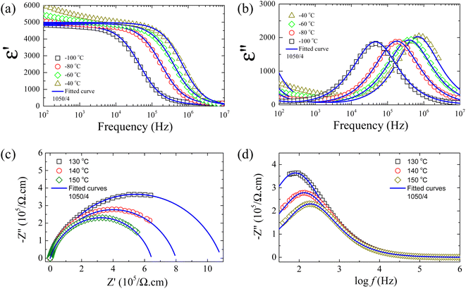 |
| | Fig. 8 (a and b) Real part (dielectric permittivity, ε′) and imaginary part (dielectric loss, ε′′) of the complex dielectric permittivity (ε*) at different temperatures for [NST]CTO ceramic sintered at 1050 °C for 4 h fitted by eqn (9). (c and d) Z* plots and −Z′′ as a function of frequency at different temperatures for [NST]CTO ceramic sintered at 1050 °C for 4 h fitted by eqn (10). | |
Just as with eqn (9), eqn (3) can be more accurately represented using a modified model, expressed as:
| |
 | (10) |
where 0 <
α1,2 ≤ 1. In an ideal IBLC microstructure,
α1,2 = 1. As depicted in
Fig. 7, when the temperature increased, the semicircular arc related to grain boundaries moved into the measured frequency range. Conversely, the peaks that represented the grains moved out of this range. Thus,
Z* was aptly modeled using a singular
RgbCgb parallel circuit, as denoted by the second term of
eqn (10). As demonstrated in
Fig. 8(c) and (d), the
Z* plots and the frequency dependence of
Z′′ at 130–150 °C for the 1050/4 samples aligned well with the predictions of
eqn (10). Below 130 °C, the data could not be accurately fitted as the
Z′′ shifted outside the lowest limited frequency range. This is because when fitting the impedance data of a giant dielectric material with an IBLC microstructure, the diameter of the semicircular arc and the peak position of −
Z′′ were governed by the corresponding
R and
C values, respectively. Based on the fitted results, the
Cgb values at higher temperatures slightly increased to ∼1.3–1.8 nF compared to a low temperature range, with
α2 values ranging from 0.75 to 0.79. The fitting of the dielectric and impedance data unambiguously confirmed that the giant dielectric properties were governed by the electrical characteristics of both the grains and grain boundaries that together formed the IBLC structure, consistent with the Maxwell–Wagner polarization relaxation model.
In addition to their pronounced dielectric properties, which are favorable for applications in ceramic capacitors, the [NST]CTO ceramics demonstrate distinct nonlinear characteristics in their J–E relationships. This makes them promising materials for use in varistors,41 a potential vividly illustrated in Fig. 9. The specific parameters Eb and α have been comprehensively evaluated and the results have been consolidated in Table 2. Notably, the 1020/4 and 1030/4 samples exhibit the highest Eb values, a phenomenon attributed to their smaller grain sizes and a significant presence of pores within the bulk ceramics. Despite the high Eb and α values observed, the practical applicability of these materials is somewhat limited. The 1040/8 sample stands out with a considerably higher α value when juxtaposed with other members of the ACu3Ti4O12 family, showcasing a dense microstructure which augments its potential applications. This nonlinear behavior predominantly arises from the development of potential barrier height at the grain boundaries, occurring in conjunction with the semiconductor grains present.41,42 Furthermore, the presence of the CuO/Cu2O phase that tends to segregate along the grain boundaries enhances grain boundary resistance as well as intrinsic properties,35 amplifying the nonlinear characteristics of the ceramics. This not only enhances their performance but also positions [NST]CTO ceramics as superior alternatives to the members of the ACu3Ti4O12 compounds.8,20,34,35
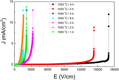 |
| | Fig. 9 J–E characteristics at 25 °C for all sintered ceramics. | |
In addition to their potential applications in capacitor and varistor devices, the humidity-sensing properties of [NST]CTO ceramics were also studied. The capacitance (Cp) as a function of RH was investigated at 25 °C, ranging from 30% to 90% RH. Fig. 10(a)–(d) show the Cp values of the 1040/8, 1050/1, 1050/2, and 1050/4 samples, respectively. The Cp values of the 1040/8 sample are independent of humidity over the measured range. Specifically, a notable trend emerged wherein the Cp values exhibited an increase in response to rising humidity levels at low frequencies for the 1050/1, 1050/2, and 1050/4 samples. This finding suggests the potential for these sintered ceramics to be employed as humidity-sensing devices. This heightened responsiveness was particularly conspicuous at frequencies ranging from 40 to 1 kHz.24 Changes in Cp with humidity are similar to those reported in previous works.24,25 In the case of ceramic-based humidity sensors,29,43 H2O molecules in the air chemisorb onto the oxide surfaces, forming the initial layer and creating two hydroxyl ions. Subsequently, additional layers of H2O molecules are physically adsorbed as multilayers, wherein the molecules in these layers are singly bonded.
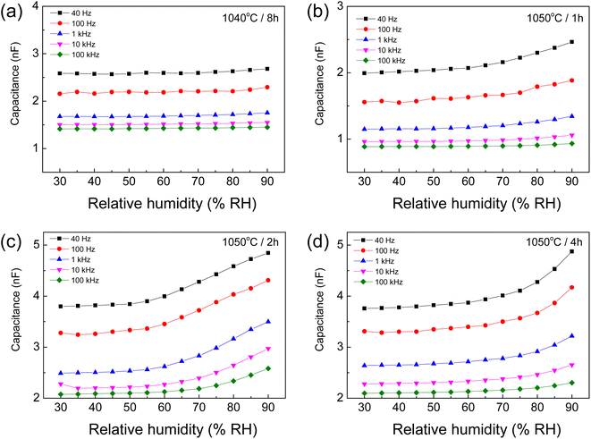 |
| | Fig. 10 Humidity dependence of capacitance at 25 °C (40 Hz to 100 kHz) of [NST]CTO sintered at (a) 1040 °C for 8 h, (b) 1050 °C for 1 h, (c) 1050 °C for 2 h, and (d) 1050 °C for 4 h. | |
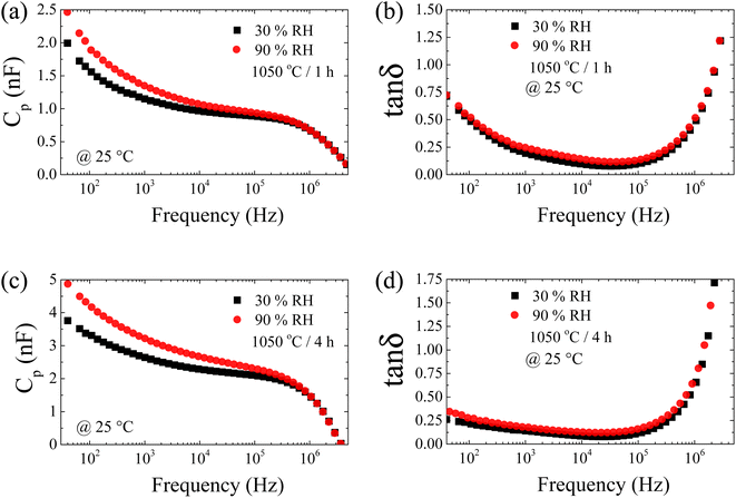
As mentioned above, the changes in Cp in response to humidity are likely caused by the physisorbed H2O on the surface of [NST]CTO.25 Consequently, the dielectric response of [NST]CTO in a low-frequency range (usually lower than 103 Hz) originates from the surface barrier layer capacitor (SBLC) effect.38,44 To further understand this, we examined the frequency dependence of Cp and tanδ at both 30% and 90% RH. As illustrated in Fig. 11(a) and (c), the Cp values for the 1050/1 and 1050/4 samples at 90% RH exceed those at 30% RH across the frequency range of 40–105 Hz. This observation implies that in addition to the SBLC effect, the IBLC effect is likely more pronounced and plays a significant role in this phenomenon. Fig. 11(b) and (d) reveal that the tanδ values of the 1050/1 and 1050/4 samples at both 30% and 90% RH are nearly identical, with only minor variations in tanδ observed. This suggests that [NST]CTO ceramics might be more suitable for capacitive-type sensors rather than resistive-type sensors. Furthermore, this indicates that variations in Cp with humidity are largely attributed to the IBLC effect. This is because a notable change in the low-frequency Cp value due to the SBLC effect typically accompanies a significant shift in tanδ.45 For Mg-doped CCTO ceramics,25 H2O molecules are also absorbed on grain boundaries. This absorption can elevate the capacitance of the grain boundary due to the accumulation of more charges, leading to an increased ε′ (or Cp) value across the 40–105 Hz frequency range compared to values at 30% RH. When AC electric fields are applied, the physisorbed H2O molecules can align themselves with the direction of the electric field, giving rise to polarization and influencing the Cp value.46 In a low-frequency range, the direction of the electric field changes more slowly compared to a high-frequency range. As such, the intensity of polarization, owing to the orientation of physisorbed H2O molecules, can be more easily accumulated than in a high-frequency range, where the direction of the electric field alters before rotation is completed.
 |
| | Fig. 11 Frequency dependence of capacitance (Cp) and loss tangent (tanδ) at 30 and 90 RH% for [NST]CTO sintered (a and b) 1050 °C for 1 h and (c and d) 1050 °C for 4 h. | |
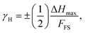
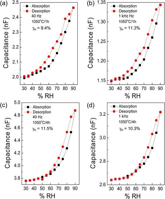
To delve deeper into the potential application of [NST]CTO as humidity sensors, we evaluated the hysteresis errors (γH) at frequencies of 40 and 1 kHz in samples sintered at 1050 °C under various ts conditions, as depicted in Fig. 12(a)–(d). The γH is calculated using the following equation:25,29
| |
 | (11) |
where
FFS and Δ
Hmax represent the full-scale output and the maximum different outputs between forward and backward operations, respectively. The
γH values are summarized in
Table 2. The
γH value for the 1050/1 sample was the lowest observed. In the case of CCTO ceramic sintered at 1100 °C, it has been reported that the
γH value reached 20.1%.
25 Meanwhile, the
γH values for the CCTO ceramics sintered at 1020 and 1050 °C were 9.2% and 15%, respectively.
25 Consequently, the [NST]CTO ceramics demonstrate promising potential for use in humidity sensors.
 |
| | Fig. 12 Hysteresis loop of capacitance at 40 Hz and 1 kHz (25 °C) of [NST]CTO sintered at (a and b) 1050 °C for 1 h and (c and d) 1050 °C for 4 h. | |
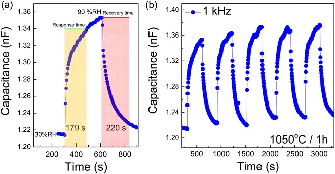
Moreover, the response and recovery times were accurately measured and calculated. The time required to attain 90% of the total change is defined as the response time in the case of adsorption and the recovery time in the case of desorption. The response and recovery characteristics of the 1050/1 sample (1 kHz) are depicted in Fig. 13(a). The response and recovery times are approximately 179 s (∼3 min) and 220 s (∼3–4 min), respectively. In comparison, the CCTO ceramic sintered at 1100 °C exhibited response and recovery times of 13 and 30 min, respectively, while the CCTO ceramic sintered at 1020 °C displayed times of about 13.7 and 3.9 min, respectively.25 For the CaCu2.6Mg0.4Ti4O12, the sample's response and recovery times are roughly 14.3 min and 20 min, respectively.25 Furthermore, the experiments showed good repeatability in continuous measurements, Fig. 13(b). Consequently, the [NST]CTO ceramics demonstrate promising potential for use in humidity sensors. In conclusion, this research introduces a new perovskite functional oxide that exhibits a wide range of promising properties, making it suitable for applications in ceramic capacitors, varistors, and humidity sensors. Table 3 details a comparative analysis of nonlinear and humidity sensing parameters for [NST]CTO ceramics in relation to earlier studies. Notably, [NST]CTO demonstrated favorable parameters, particularly a lower Ts, when compared to other giant dielectric oxides. This research suggests that [NST]CTO could serve as an alternative choice in the realm of giant dielectric oxides, especially if its properties are further optimized to meet application-specific requirements.
 |
| | Fig. 13 (a) Response and recovery times and (b) repeatability of [NST]CTO sintered at 1050 °C for 1 h. | |
Table 3 Comparative analysis of nonlinear (Eb and α) and humidity sensing parameters (γH, response time (tres), and recovery time (trec)) between [NST]CTO ceramics and previous studies
| Ceramics |
Non-linear properties |
Humidity sensing properties |
Ref. |
| Eb (V cm−1) |
α |
Tres (min) |
Trec (min) |
γH (%) |
| Humidity sensing properties were measured at 103 Hz. Humidity sensing properties were measured at 102 Hz. |
| CCTO sintered at 1100 °Ca |
— |
— |
13 |
30 |
20.1 |
25 |
| CCTO sintered at 1020 °Ca |
— |
— |
13.7 |
3.9 |
9.2 |
25 |
| CaCu2.6Mg0.4Ti4O12 sintered at 1100 °Ca |
— |
— |
14.3 |
20 |
7 |
25 |
| 5%(Na,Nb) co-doped TiO2 sintered at 1350 °Cb |
— |
— |
∼1.9 |
∼0.3 |
4.2 |
47 |
| 10%(In,Nb) co-doped TiO2 sintered at 1400 °Cb |
— |
— |
2.75 |
0.5 |
7.3 |
48 |
| Ca0.775Tb0.15Cu3Ti4O12 sintered at 1070 °C |
1.5 × 10⁴ |
29.7 |
— |
— |
— |
31 |
| Na1/3Ca1/3Bi1/3Cu3Ti4O12 sintered at 1080 °C |
8.4 × 10² |
3.2 |
— |
— |
— |
20 |
| Ca0.7Sr0.3Cu3Ti4O12 sintered at 1000 °C |
1.1 × 10⁴ |
6.8 |
— |
— |
— |
4 |
| Na1/2Sm1/2Cu3Ti4O12 sintered at 1100 °C |
2.2 × 10³ |
6.1 |
— |
— |
— |
34 |
| 1%SnO2-CCTO/CaTiO3 sintered at 1100 °C |
2.3 × 10⁴ |
7 |
— |
— |
— |
49 |
|
| [NST]CTOa sintered at 1020–1050 °C |
| 1020/4 |
1.7 × 10⁴ |
127 |
— |
— |
— |
In this work |
| 1030/4 |
1.3 × 10⁴ |
45 |
— |
— |
— |
| 1050/4 |
2.3 × 10³ |
6 |
∼1.8 |
∼3.7 |
10.3 |
| 1050/1 |
1.5 × 10³ |
7 |
∼3 |
∼3.6 |
11.3 |
4. Conclusions
We successfully synthesized and analyzed a novel perovskite compound, [NST]CTO, via the solid-state reaction method. Our comprehensive investigation into its giant dielectric response, nonlinear characteristics, and humidity-sensing properties has illuminated its significant potential in various applications. The compound exhibited a noteworthy giant dielectric response, with ε′ values of ∼2800–6000, dependent upon specific sintering conditions utilized during the preparation process. This finding hints at the possibility of further enhancing its functional attributes through optimization of the sintering parameters, thereby expanding its potential uses in electronic and sensor technologies. Furthermore, the material demonstrated pronounced nonlinear J–E characteristics at room temperatures, with a considerable range observed in the α values. This nonlinear behavior, linked to the ceramic microstructures, opens up avenues for its inclusion in devices seeking to modulate electrical responses with precision. Additionally, our exploration of the humidity-sensing properties of the [NST]CTO material unveiled a significant variation in dielectric permittivity in response to alterations in RH. The observed hysteresis error and response/recovery times accentuate the versatility of this material, indicating its potential suitability in humidity sensing technologies.
Conflicts of interest
There are no conflicts to declare.
Acknowledgements
This research was supported by the Fundamental Fund of Khon Kaen University and the National Science, Research, and Innovation Fund (NSRF). This research work was also supported by the Research and Graduate Studies Office of Khon Kaen University. S. Srilarueang extends her gratitude to the Research and Graduate Studies Office of Khon Kaen University for the MSc scholarship provided through the Research Program.
References
- M. A. Subramanian, D. Li, N. Duan, B. A. Reisner and A. W. Sleight, J. Solid State Chem., 2000, 151, 323–325 CrossRef CAS.
- C. C. Homes, T. Vogt, S. M. Shapiro, S. Wakimoto and A. P. Ramirez, Science, 2001, 293, 673–676 CrossRef CAS PubMed.
- W. Hao, P. Xu, P. Han and M. Wang, J. Eur. Ceram. Soc., 2023, 43, 986–992 CrossRef CAS.
- J. Zhao, L. Sun, E. Cao, W. Hao, Y. Zhang and L. Ju, Appl. Phys. A: Mater. Sci. Process., 2022, 128, 340 CrossRef CAS.
- G.-T. Miao, Z.-J. Wang, P. Li, J.-G. Hao, W. Li, J. Du, W.-F. Han, C.-M. Wang, G.-R. Li and P. Fu, J. Asian Ceram. Soc., 2022, 10, 165–177 CrossRef.
- J. Tan, Y. Guo, F. Ren and J. Zhao, J. Am. Ceram. Soc., 2023, 106, 3462–3470 CrossRef CAS.
- J. Liu, C.-G. Duan, W.-G. Yin, W. Mei, R. Smith and J. Hardy, Phys. Rev. B: Condens. Matter Mater. Phys., 2004, 70, 144106 CrossRef.
- P. Thongbai, J. Jumpatam, B. Putasaeng, T. Yamwong and S. Maensiri, J. Appl. Phys., 2012, 112, 114115 CrossRef.
- T. B. Adams, D. C. Sinclair and A. R. West, Adv. Mater., 2002, 14, 1321–1323 CrossRef CAS.
- D. C. Sinclair, T. B. Adams, F. D. Morrison and A. R. West, Appl. Phys. Lett., 2002, 80, 2153 CrossRef CAS.
- R. Schmidt, M. C. Stennett, N. C. Hyatt, J. Pokorny, J. Prado-Gonjal, M. Li and D. C. Sinclair, J. Eur. Ceram. Soc., 2012, 32, 3313–3323 CrossRef CAS.
- T. Adams, D. Sinclair and A. West, Phys. Rev. B: Condens. Matter Mater. Phys., 2006, 73, 094124 CrossRef.
- Y. Lin, L. Jiang, R. Zhao and C.-W. Nan, Phys. Rev. B: Condens. Matter Mater. Phys., 2005, 72, 014103 CrossRef.
- M. A. Subramanian and A. W. Sleight, Solid State Sci., 2002, 4, 347–351 CrossRef CAS.
- Z. Peng, D. Wu, P. Liang, X. Zhou, J. Wang, J. Zhu, X. Chao and Z. Yang, J. Am. Ceram. Soc., 2020, 103, 1230–1240 CrossRef CAS.
- Z. Peng, J. Wang, X. Zhou, J. Zhu, X. Lei, P. Liang, X. Chao and Z. Yang, Ceram. Int., 2020, 46, 14425–14430 CrossRef CAS.
- Z. Peng, J. Wang, X. Lei, J. Zhu, S. Xu, P. Liang, L. Wei, D. Wu, J. Wang, X. Chao and Z. Yang, Mater. Chem. Phys., 2021, 258, 123940 CrossRef CAS.
- P. Saengvong, N. Chanlek, P. Srepusharawoot, V. Harnchana and P. Thongbai, J. Am. Ceram. Soc., 2022, 105, 3447–3455 CrossRef CAS.
- Y. Su and Y. Wang, Appl. Phys. A: Mater. Sci. Process., 2016, 122, 1–7 CrossRef CAS.
- P. Kum-onsa, P. Thongbai, B. Putasaeng, T. Yamwong and S. Maensiri, J. Eur. Ceram.
Soc., 2015, 35, 1441–1447 CrossRef CAS.
- Z. Peng, J. Wang, P. Liang, J. Zhu, X. Zhou, X. Chao and Z. Yang, J. Eur. Ceram. Soc., 2020, 40, 4010–4015 CrossRef CAS.
- Y. Liu, X. Zhao and C. Zhang, J. Mater. Sci.: Mater. Electron., 2016, 27, 11757–11761 CrossRef CAS.
- Z. Peng, X. Zhou, J. Wang, J. Zhu, P. Liang, X. Chao and Z. Yang, Ceram. Int., 2020, 46, 11154–11159 CrossRef CAS.
- M. Li, Sens. Actuators, B, 2016, 228, 443–447 CrossRef CAS.
- M. Li, X. L. Chen, D. F. Zhang, W. Y. Wang and W. J. Wang, Sens. Actuators, B, 2010, 147, 447–452 CrossRef CAS.
- A. Chattopadhyay and J. Nayak, Sens. Actuators, A, 2022, 341, 113603 CrossRef CAS.
- S. Tachibana, Y.-F. Wang, T. Sekine, Y. Takeda, J. Hong, A. Yoshida, M. Abe, R. Miura, Y. Watanabe, D. Kumaki and S. Tokito, ACS Appl. Mater. Interfaces, 2022, 14, 5721–5728 CrossRef CAS PubMed.
- J. Wang, Y. M. Guo, S. T. Wang, L. Tong, J. Sun, G. B. Zhu and C. C. Wang, J. Eur. Ceram. Soc., 2019, 39, 323–329 CrossRef CAS.
- T. Y. Li, R. J. Si, J. Sun, S. T. Wang, J. Wang, R. Ahmed, G. B. Zhu and C. C. Wang, Sens. Actuators, B, 2019, 293, 151–158 CrossRef CAS.
- T. Ishihara and S. Matsubara, J. Electroceram., 1998, 2, 215–228 CrossRef CAS.
- P. Thongbai, J. Boonlakhorn, B. Putasaeng, T. Yamwong and S. Maensiri, J. Am. Ceram. Soc., 2013, 96, 379–381 CrossRef CAS.
- D.-Y. Lu, X.-Y. Yu and J.-W. Liu, Ceram. Int., 2017, 43, 8664–8676 CrossRef CAS.
- D. E. Macphee, D. C. Sinclair and S. L. Cormack, J. Am. Ceram. Soc., 1997, 80, 2876–2884 CrossRef CAS.
- W. Somphan, P. Thongbai, T. Yamwong and S. Maensiri, Mater. Res. Bull., 2013, 48, 4087–4092 CrossRef CAS.
- P. Leret, J. F. Fernandez, J. de Frutos and D. Fernández-Hevia, J. Eur. Ceram. Soc., 2007, 27, 3901–3905 CrossRef CAS.
- W. Yuan, J. Phys. D: Appl. Phys., 2009, 42, 175401 CrossRef.
- J. Wu, C.-W. Nan, Y. Lin and Y. Deng, Phys. Rev. Lett., 2002, 89, 217601 CrossRef PubMed.
- M. Li, Z. Shen, M. Nygren, A. Feteira, D. C. Sinclair and A. R. West, J. Appl. Phys., 2009, 106, 104106 CrossRef.
- P. Lunkenheimer, S. Krohns, S. Riegg, S. G. Ebbinghaus, A. Reller and A. Loidl, Eur. Phys. J.: Spec. Top., 2010, 180, 61–89 Search PubMed.
- F. Greuter and G. Blatter, Semicond. Sci. Technol., 1990, 5, 111 CrossRef CAS.
- D. R. Clarke, J. Am. Ceram. Soc., 1999, 82, 485–502 CrossRef CAS.
- S.-Y. Chung, I.-D. Kim and S.-J. L. Kang, Nat. Mater., 2004, 3, 774–778 CrossRef CAS PubMed.
- E. Traversa, Sens. Actuators, B, 1995, 23, 135–156 CrossRef CAS.
- M. Li, D. C. Sinclair and A. R. West, J. Appl. Phys., 2011, 109, 084106 CrossRef.
- W. Tuichai, S. Danwittayakul, N. Chanlek, P. Srepusharawoot, P. Thongbai and S. Maensiri, RSC Adv., 2017, 7, 95–105 RSC.
- K.-C. Kao, Dielectric phenomena in solids: with emphasis on physical concepts of electronic processes, Academic Press, Amsterdam, Boston, 2004 Search PubMed.
- T. Li, R. Si, J. Wang, S. Wang, J. Sun and C. Wang, J. Am. Ceram. Soc., 2019, 102, 6688–6696 CrossRef CAS.
- R. J. Si, T. Y. Li, J. Sun, J. Wang, S. T. Wang, G. B. Zhu and C. C. Wang, J. Mater. Sci., 2019, 54, 14645–14653 CrossRef CAS.
- G. Cotrim, J. A. Cortés, H. Moreno, S. M. Freitas, M. V. S. Rezende, L. R. O. Hein and M. A. Ramírez, Mater. Charact., 2020, 170, 110699 CrossRef CAS.
|
| This journal is © The Royal Society of Chemistry 2023 |
Click here to see how this site uses Cookies. View our privacy policy here. 
 Open Access Article
 This Open Access Article is licensed under a Creative Commons Attribution-Non Commercial 3.0 Unported Licence
 *ac
*ac


 is the permittivity of bulk material, and ϕb is the potential barrier height at the grain boundary. On the other hand, as shown in Fig. 7(b), a surge in Ts to 1050 °C led to a substantial reduction in Rg, ranging between 0.2 and 0.4 kΩ cm. This shift resulted in further enhanced ε′ values for the 1050/2 and 1050/4 specimens, exceeding the 1040/5 sample. Adams et al.9 observed that, around room temperature, a CCTO ceramics Z* plot displayed only a nonzero intercept without any evident semicircular arc in the lower MHz region. They attributed this behavior to the electrical response of the semiconducting grains. Later, Sinclair et al.,10 conclusively demonstrated that a semicircular arc become visible at temperatures around −100 °C. This observation aligned with what was seen in the [NST]CTO ceramics, as highlighted in the inset of Fig. 7(b).


 and
and 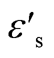 denote the dielectric permittivities at low and high frequency respectively. τ is a relaxation time. The last term reflects the impact of conductivity on energy loss.


 σ′ = 1/C0Rgb, and τ = RgCgb, respectively. Eqn (4) was derived from an ideal RgbCgb parallel circuit corresponding to a perfect IBLC microstructure. However, such an ideal IBLC microstructure is theoretical and does not exist in practice. Consequently, the dielectric and impedance data can be more accurately described using a modified model, as illustrated in the subsequent equation:


