DOI:
10.1039/D3RA06140J
(Paper)
RSC Adv., 2023,
13, 32282-32295
(Mg,Mn)-dual doping synergism towards luminescence and electrical properties of ZnO/p-Si heterojunction diodes†
Received
9th September 2023
, Accepted 26th October 2023
First published on 2nd November 2023
Abstract
In this study, we investigated the impact of divalent dual dopants on ZnO by examining the structural and spectroscopic properties of (Mg,Mn)-doped ZnO thin films deposited using spray deposition technique. Also, we analysed the current–voltage (I–V) characteristics of (Mg,Mn)-doped ZnO/p-Si heterojunctions for potential light-emitting applications. X-ray diffraction of (Mg,Mn)-doped ZnO on glass substrates reveals a compression along the c-axis and a reduction in crystallite size compared to the Mn-doped ZnO film. Moreover, the band gap of Mn-doped ZnO samples increases from 3.29 eV to 3.35 eV with the addition of the Mg dopant. The optical disorder, as estimated through the Urbach tail, increases from 0.33 eV to 0.5 eV with an incremental increase in the concentration of Mg. XPS studies confirmed the substitution of Mn2+ and Mg2+ into Zn2+ in MnMg:ZnO samples. A dominant color of yellow with wavelength 585 nm was recorded, suitable for yellow emitting devices. In the set of fabricated heterojunctions of MnMg:ZnO/Si, 2 at% Mg doped MnZnO film showed a low knee voltage of ∼1.8 V. It was observed that all the MnMg:ZnO/p-Si heterojunctions showed good rectifying behaviour. Various diode parameters were found using transport models such as TE and Norde, wherein a barrier height of ∼0.6–0.7 eV and an ideality factor in the range of ∼1.5–3 was observed. Retention of good crystallinity, slight band gap tuning, apt barrier height, low sheet resistance, and better emission properties were identified for the prepared MgMn:ZnO thin films that find application in optoelectronic devices.
1 Introduction
Zinc oxide, one of the most widely explored n-type metal oxide semiconductor materials, finds application in various optoelectronic devices with its unique material properties in conjugation with inexpensiveness, non-toxicity, and natural abundance. However, pure ZnO is unstable due to thermal edging or corrosive environment and the presence of point defects makes it resistive.1 To stabilize the ZnO system and widen the potential application of ZnO, suitable dopants that bring out the required changes in the properties of ZnO are of research interest. The direct wide band gap of ZnO can be modulated by doping, from which the electronic properties are controlled. II/III group elements are doped to boost the constancy and performance of ZnO. The properties of the ZnO thin films doped with different dopants have been extensively studied over the decades. However, co-doping of ZnO is less reported and the study of the effect of dual doping is unmapped. Most of the literature reports on the group-III elements doped ZnO that enhance the conductivity.2 Codoping in ZnO using various elements such as (Al,Fe),3 (Al,Sc),4 (Al,Ga),5 (Ga,B),6 (Fe,Al),7 (Al,F),2 (N,Cu),8 (Ag,N),9 (F,Ga),10 (Mn,Co),11 (Li,Er),12 (Al,Co),13,14 (Co,Cu),15 (N–Al),13 (In,N),16 (Li,N),17 (Ag,N)18 and (Ce,Al)19 have been reported for LED, ferromagnetism, ammonia detection, transparent conducting material, optoelectronic, perovskite solar cells, luminescence, magnetic, p-type and electric device applications. Amongst the applications, LED attracts more attention because of its advantages over conventional light sources. A variety of elements such as gallium, indium, and arsenic have been used to fabricate LED. Tin and zinc which are less expensive are also used in LEDs. It is noteworthy to mention the fact that many optoelectronic properties of ZnO are fairly similar to that of GaN, which is typically used for LED fabrication20 such as ZnO,21 ZnO:Ga,22 and Mg, Ce:ZnO.23 From the literature, it can be comprehended that either two or three-color emitting systems are used to harvest different colors of emission in LED. So, by the combination of different dopants having emissions in entirely different ranges, the emission of the final device could be tuned. ZnO has emission in the UV region (∼370 nm).24 Reports mention the difficulties in obtaining lighter colors in as-deposited ZnO.25–27 It is observed that upon co-doping ZnO with divalent impurities, the concentration of intrinsic defects such as oxygen vacancy, interstitial Zn, and antisite oxygen varies,28 resulting in different emission than that of the host.11 Mg is a known dopant for the enhancement of the band gap of the host, with a wide emission in the wavelength range of 550–650 nm (green-red).27,29 ZnOMg2+ and Zn2+ have similar ionic radii because of which the lattice distortion can be minimal. Also, the electrical behaviours of ZnO diodes were significantly enhanced by the incorporation of Mg2+ into ZnO with a high rectifying ratio and low dark current.30 Similarly rectifying nature was observed in Mn doped ZnO prepared on silicon substrates,31 and has emission in the blue wavelength region.24,26 Therefore, with the Mg dopant covering green to red emission, and Mn dopant covering the blue regime of the visible spectrum, the suitable mixture of the two dopants is expected to give a color coordinate more towards 0.33 when compared to the reported color coordinates of ZnO thin films, (0.155, 0.032).32 While choosing the dopant concentration, it is to be noted that the solubility of MgO in ZnO is minimal at high dopant levels.33 Similarly, when the Mn dopant level is higher than the critical level, which is nearly 2 at%, the luminescence properties are quenched.34 Therefore, fixing the low level of the Mg and Mn dopant concentration is required to avoid phase separation with a high level of Mg in ZnO.35 Therefore, the Mn concentration was fixed at 2 at%, and Mg concentration increased up to 4 at%. Moreover, so far little attention is given to the group II elements dual doping on ZnO, and its spectroscopic characterization.
Both physical and chemical methods have been used for the deposition of the ZnO thin films such as physical vapor deposition,36 sputtering,37 successive ionic layer deposition,38 sol–gel,39 chemical bath deposition,38 and spray pyrolysis.40 Among the processes, spray pyrolysis is an industrially beneficial large area deposition technique. In spray pyrolysis, doping is much easier and high quality, and controlled deposition is possible, even if the dopant number is higher. The present manuscript deals with the structural, and spectroscopic studies of the (Mn,Mg) doped ZnO films. Further, Ag/(Mn,Mg)ZnO/p-Si/Ag heterojunctions were fabricated and their electrical properties were studied. Growth and device properties of (Mn,Mg):ZnO/p-Si heterojunctions are presented. I–V characteristics indicated the sufficiently high carrier concentration of (Mn,Mg):ZnO to form a p–n junction. Because of the low cost, excellent quality, and large area availability of Si wafers, integrating well-established Si electronics with ZnO based optoelectronic devices becomes industrially beneficial. Much effort is made-for to grow high quality ZnO on Si which is a challenging task for diode applications.
2 Experimental details
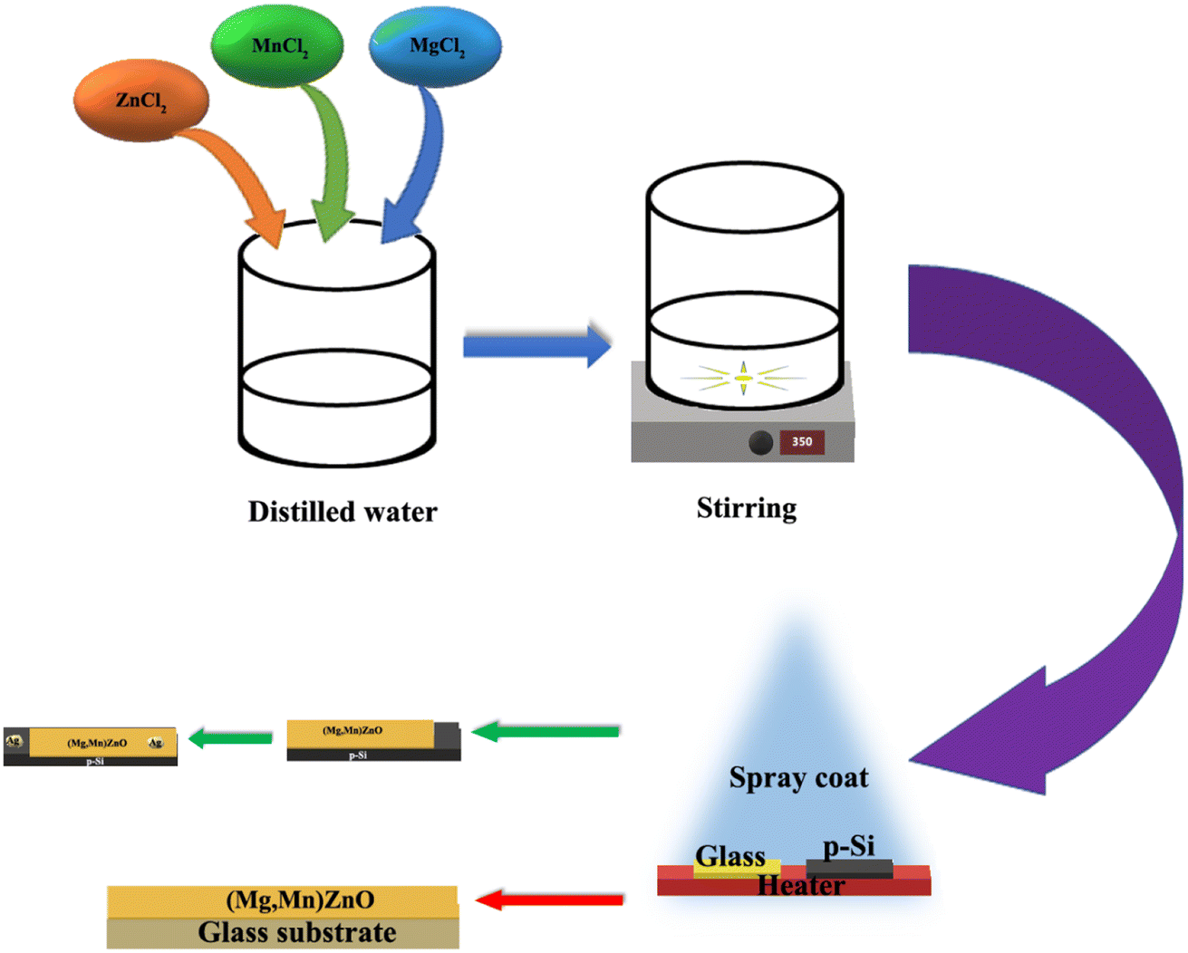
The (Mn,Mg)ZnO thin films were deposited using a computer-assisted Holmarc spray pyrolysis apparatus with various Mg dopant concentrations. Both soda lime glass and silicon substrates were placed on the substrate heater at 648 ± 5 K simultaneously. Prior to the deposition, soda lime glass was cleaned by the standard procedure of cleaning in laboline, ultrasonication in DI water, and HCl acid treatment, followed by distilled water, isopropyl alcohol, and acetone. Substrates were dried in nitrogen gas. Silicon substrates were cleaned by HF treatment. At first, substrates were thoroughly washed in ethanol flow for 15 min, followed by 2% HF treatment for 15 min. Finally, the substrates were checked for the absence of adhesive forces between the substrate and distilled water. Fig. 1 displays the schematics of the steps involved in spray coating of the samples. At a spray rate of 1 ml min−1, 0.05 M stock solution of Manganese chloride in water, magnesium chloride in water, and zinc chloride in water were sprayed to make up to 0.6 μm thick film on the glass substrate. The thickness was estimated using the Bruker stylus profilometer. At the same time, HF cleaned 2.5 × 2.5 mm p-silicon substrates were used to fabricate heterojunction. The silver contacts for the diodes were made using the physical vapor deposition method. Samples have been named as S0, S1, S2, S3, and S4 for 0 at%, 1 at%, 2 at%, 3 at%, and 4 at% Mg doped Mn0.02Zn0.98O thin films on soda lime glass. Similarly, the films on silicon substrates are named M0, M1, M2, M3, and M4 respectively.
 |
| | Fig. 1 Schematics of experimental details of heterojunction formation. | |
Structural properties of the samples are analysed using X-ray diffractogram (XRD) (Rigaku SmartLab) with Cu Kα (λ = 1.504 Å) radiation. Surface morphology was characterized using a scanning electron microscope (SEM) (ZEISS), linked with energy dispersive X-ray analysis (EDX), which was operated at an accelerating voltage of 12 kV. Transmittance spectra were recorded using a UV-vis spectrophotometer (SHIMADZU UV 1800) after nullifying the optical effect from the glass substrate. Photoluminescence (PL) spectra were recorded (Jobin Yvon FLUOROLOG-FL3-11) using a Xenon lamp, and PMT detector, with 0.2 nm resolution at an excitation wavelength of 320 nm. Raman spectra (Horiba Jobin Yvon HR800-UV) were recorded with an excitation source of 532 nm and an Olympus BX41 confocal micro-Raman spectrometer. XPS (PHI 5000 VersaProbe III) recording was carried out using a C60 ion gun and X-ray source of Al Kα 1486.6 eV with a step size of 0.05 eV. Current–voltage (I–V) curves for the (Mn,Mg)ZnO/p-Si diodes were recorded by Keithley 2450 source meter.
3 Results and discussions
3.1 Surface morphology and structural properties
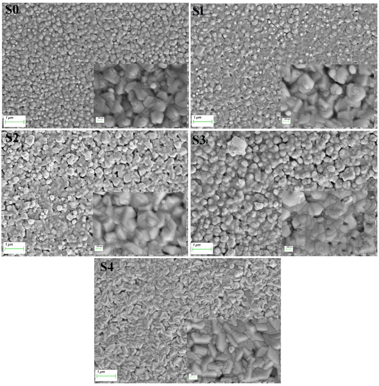
Fig. 2 displays the morphology of samples by SEM. All samples with evenly distributed grains exhibited uniform surfaces. On the surface of the samples S2 and S3, voids were observed. Mn-doped ZnO with dense granular morphology without any clusters indicates the aptness of the material surface for LED fabrication. Upon the addition of Mg, bean shapes appeared. The sizes of grains observed from the SEM are determined using the ImageJ software and are given in Table 1. The composition of elements in the samples observed from EDX is given in Table 1. Even though the Mn concentration kept constant, with the addition of Mg, Mn concentration decreased but remained nearly constant in all samples. Maintaining or controlling the stoichiometry is challenging with the increased number of elements.2
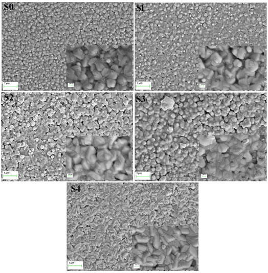 |
| | Fig. 2 Scanning electron micrographs of (Mn,Mg):ZnO thin films. | |
Table 1 Elemental composition and the grain size observed from EDX for (Mn,Mg):ZnO thin films
| Sample |
Zn |
O |
Mn |
Mg |
Mn/(Mn + Mg + Zn) |
Mg/(Mn + Mg + Zn) |
Zn/(Mn + Mg + Zn) |
Grain size (nm) |
| S0 |
42.29 |
56.86 |
0.85 |
0.00 |
0.020 |
0.000 |
0.980 |
230 |
| S1 |
44.28 |
54.1 |
0.69 |
0.93 |
0.015 |
0.020 |
0.965 |
313 |
| S2 |
46.67 |
51.66 |
0.45 |
1.21 |
0.009 |
0.025 |
0.966 |
358 |
| S3 |
44.23 |
53.85 |
0.48 |
1.44 |
0.010 |
0.032 |
0.958 |
286 |
| S4 |
46.96 |
50.25 |
0.73 |
2.06 |
0.015 |
0.041 |
0.944 |
392 |
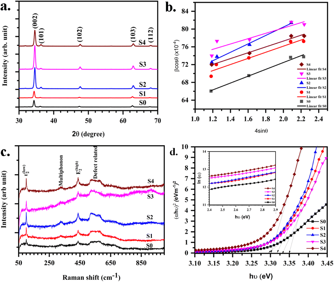
The XRD of (Mn,Mg)ZnO thin films are displayed in Fig. 3. Wurtzite ZnO is a hexagonal crystal in the space group P63mc. All the samples showed a hexagonal wurtzite structure (JCPDS card no. 80-0075) with a sharp peak corresponding to the (002) plane. Zn and O atoms stalked alternatively along the c-axis. The position of the (002) peak shifted towards higher 2θ values with the increase in Mg dopant concentration. The shift in the peak position of S1 (ESI Fig. S1†) indicates the expansion of the unit cell upon the addition of Mg into the S0.40,41 The single-phase purity with no secondary phase indicates the proper incorporation of Mn and Mg into the ZnO lattice. Scherrer equation and W–H plot (Fig. 3b) are used to determine the crystallite size. The crystallite size estimated from the two methods is given in Table 2. With the addition of Mg, the unit cell compression occurs. This can be explained based on the ionic radii of Zn2+, Mn2+, and Mg2+ as r (Mg2+) = 0.57 Å < r (Zn2+) = 0.60 Å < r (Mn2+) = 80 Å.42 Crystallite size calculated using (002) reflection decreased slightly with the addition of Mg into MnZnO. The slight decrease in the size caused by the increase of Mg doping may be due to the gradual deterioration of ZnO crystallinity, due to the lattice disorder and strain induced by the Mg2+ substitution.42 However, as the Mn2+ dopant causes higher strain due to its larger radius, on the other hand, the Mg2+ dopant with a slight difference in ionic radius in comparison with Zn2+, does not induce significant reduction of the crystallite size.
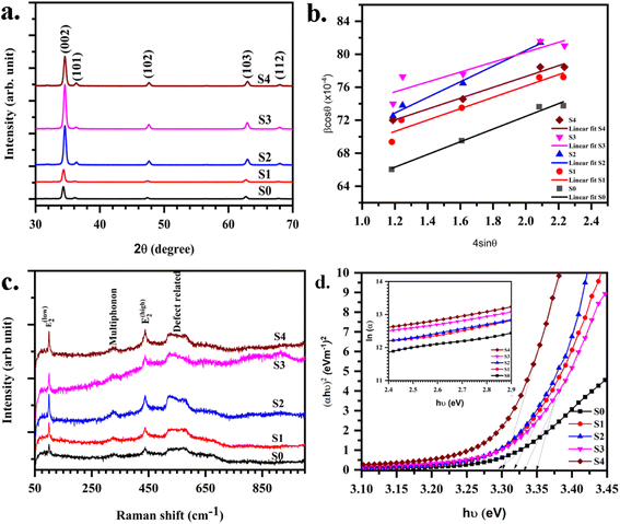 |
| | Fig. 3 (a) XRD (b) W–H plot (c) Raman spectra (d) Tauc's plot for energy band gap estimation (inset: Urbach energy plot) for (Mn,Mg):ZnO thin films. | |
Table 2 Structural parameters obtained from XRD for (Mn,Mg):ZnO thin films
| Sample |
Lattice parameter (Å) |
Cell volume V (Å)3 |
Crystallite size D (nm) |
| a = b |
c |
Scherrer |
WH |
| S0 |
3.014 |
5.220 |
47.4 |
21.0 |
24.3 |
| S1 |
3.011 |
5.215 |
47.3 |
20.0 |
22.2 |
| S2 |
2.992 |
5.183 |
46.4 |
19.0 |
22.5 |
| S3 |
2.992 |
5.183 |
46.4 |
18.7 |
20.3 |
| S4 |
2.994 |
5.186 |
46.5 |
19.2 |
20.2 |
3.2 Raman spectroscopy
Raman spectra of (Mn,Mg)ZnO thin films as a function of Mg concentration are investigated. The optical phonons of ZnO are A1 + 2B1 + 2E2 + E1, with E modes as two-fold degenerate. A1 and E1 are polar phonons that exhibit different frequencies for TO and LO modes. E2 is a non-polar mode and has two frequencies E2 high and E2 low associated with oxygen atoms and Zn sublattices. B1 is a silent mode. Raman spectra for the (Mn,Mg)ZnO films are presented in Fig. 3c. It mainly consists of low and high modes of E2 symmetry at 99 cm−1 and 437 cm−1. Raman line near 570 cm−1 corresponds to LO phonon mode with A1 symmetry. Raman line in the range of 320–330 cm−1 corresponds to either multiphonon scattering or from the sp–d interaction at defects like oxygen vacancy. The intensity of this line is low indicating the low oxygen vacancy, thereby high resistivity of the samples.11,43 A Raman line near 520 cm−1 corresponds to the Mn-related scattering and is present in the spectrum for all samples.44 S. A. Azzez et al.29 have observed the stronger and sharper E2 mode (at 437 cm−1) with the addition of Mg into the ZnO system. This revealed the better crystallization upon the Mg substitution into Zn. E2 high and low modes are associated with oxygen atoms and Zn sublattice respectively.45 Like the ref. 29, in the present Raman spectra, the intensity of the E2 mode at 437 cm−1 increased with the addition of Mg into the ZnO, and the corresponding Raman line became sharper. This indicated the improved crystallinity of MnZnO upon the addition of Mg dopant. In support, the Mn-related Raman line has shown a lowering of linewidth. This could also be due to low Mn concentration in S2, S3 and then rise for S4 samples (as observed from EDX). Raman line frequency shift in LO phonon mode and its appearance is related to the oxygen defects, interstitial zinc, and free carriers. The confinement effect of optical phonons leads to symmetry and broadening of E2 mode.46 E2 modes are nonpolar and have a low frequency mode related to heavy Zn sublattice and high frequency E2 high associated with oxygen atoms only.45 The origin of the A1 LO mode is due to the zinc interstitial defect.44
3.3 Optical properties
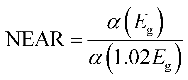
Mg dopant eases band gap widening. The optical band gap of each sample was estimated by employing Tauc's relation. From the (αhν)2 vs. hν graph (Fig. 3d), where α is the absorption coefficient, hν is the incident energy of the photon, the band gap for all samples measured. The band gaps of MgO (7.8 eV)47 and MnO (4.2 eV)24 are much higher than that of ZnO (3.2 eV).11 Therefore, the addition of Mg and Mn into the ZnO is expected to increase its band gap. However, there is an anomalous variation in the energy band gap with the variation in dopant concentration as given in Table 3. For the short-range, paramagnetic phase of Mn in ZnO, band gap bowing could be explained by the second-order perturbation theory. The intense interaction between d electrons of Mn and s or p electrons of the host bands should be considered. Independent of temperature, the exchange constant involving s-states reduces the conduction band bottom level, and p-states raise the top level of the valence band.48 Thus, the band gap of the material varied with the Mn concentration. i.e., a small increment in the Mn concentration decreased the band gap. The electron in the uppermost level of the valence band gets excited by the absorption of the photon into the lowermost level of the conduction band. Amorphous solids or thermal vibrations or defect centres induce disorder in these electrons. As a result, the density state of electrons along the band edges tails towards the band gap, known as Urbach tailing. The significance of this tailing is quantified using the NEAR49| |
 | (1) |
Table 3 Optical parameters obtained from the UV-vis spectroscopy
| Sample |
Transmittance |
Band gap (eV) |
NEAR |
Urbach energy (eV) |
| S0 |
86 |
3.29 |
0.54 |
0.33 |
| S1 |
78 |
3.32 |
0.60 |
0.33 |
| S2 |
78 |
3.35 |
0.60 |
0.42 |
| S3 |
72 |
3.33 |
0.58 |
0.44 |
| S4 |
69 |
3.30 |
0.51 |
0.51 |
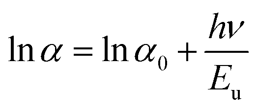
Samples with NEAR value approaching 0 are less defective, and that towards 1 are high defective. NEAR for samples was found in the range 0.5 to 0.6; therefore, a significant band tailing is present in the band gap. The, Urbach energies Eu for samples were calculated using
| |
 | (2) |
A plot of ln![[thin space (1/6-em)]](https://www.rsc.org/images/entities/char_2009.gif) α vs. hν as shown in Fig. 3d inset. The Urbach energies for samples lie in between a minimum of 0.33 eV for S1 to a maximum of 0.5 eV for S4.
α vs. hν as shown in Fig. 3d inset. The Urbach energies for samples lie in between a minimum of 0.33 eV for S1 to a maximum of 0.5 eV for S4.
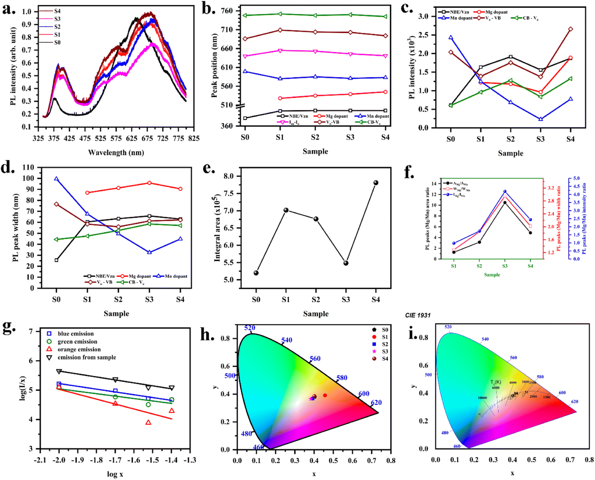
3.4 Photoluminescence
The presence of point defects in the thin film was identified by recording the PL spectra (Fig. 4a). Emission spectra for all the samples were recorded to study the effect of the dopant on the color and defect properties of ZnO. In general, PL spectra consist of near band edge (NBE) and other defect-related emissions. After baseline, the present spectra are deconvoluted to arrive at the emission characteristics. Free exciton recombination yields emission at 380 nm for Mn-doped ZnO. The transition of an electron from the conduction band to the zinc vacancy could result in an emission at 400 nm.50 Doped films in the present study are zinc deficient. Therefore, this emission is assigned to zinc vacancy. Visible emission originated from intrinsic and extrinsic defects like vacancies, interstitials, and dopants. Green emission observed in the wavelength range of 530–540 nm is assigned to Mg dopant. Moreover, Cheol Hyoun Ann et al.51 have reported the green emission from the oxygen-deficient ZnO sample, attributed to the oxygen vacancy. Bixia Lin et al.50 have reported the emission at 544 nm in ZnO to the oxygen interstitials. However, all doped films in the present study are zinc deficient, and the peak corresponding to the green emission in the 530–540 nm range does not shift according to oxygen composition (Fig. 4b). However, the peak shifted towards a higher wavelength with the Mg concentration. Therefore, it is evident that the green emission originated from the level corresponding to the extrinsic Mg dopant defect. Red emission observed at 700 nm is due to the transition of electrons from oxygen vacancy to the valence band.21 Similarly, the emission at 750 nm corresponds to the transition of an electron from the conduction band to the oxygen vacancy.21 The orange emission observed in all samples in the range of 580–600 nm corresponds to the Mn dopant. The emission at 640 nm corresponds to the transition between Zn and O interstitials.51 It could be observed that for the MnZnO sample, the orange emission was very high. As Mg was doped into the MnZnO, the intensity of the orange emission decreased. The intensity of the blue emission peak increased with the Mg dopant. The intensity of the red emission peak also increased with the Mg dopant. The intensity of both the peaks at 700 nm and 750 nm was low for MnZnO film (Fig. 4c). The oxygen content for this film was higher than any other sample in the series. As Mg was introduced, the oxygen content was observed to decrease, meanwhile the intensity of the red emission increased. Therefore, the explanation for the red emission based on the transition between bands and oxygen vacancy is well evident. PL peak width corresponding to the Mg dopant sightly increased with Mg concentration; at the same time, the peak width of Mn-related orange emission had a decreasing trend. This indicates that the green emission from the Mg dopant increases at the cost of the orange emission from Mn defects. The blue emission peak width nearly remained constant, indicating the presence of zinc vacancy. Peak widths of the red emission slightly varied according to oxygen composition (Fig. 4d). The variation in the area and the ratios of the intensities are given in Fig. 4e and f.
 |
| | Fig. 4 (a) PL spectra, variation in (b) peak position (c) intensity (d) width (e) area observed from the deconvoluted PL spectra with the variation in Mg concentration (f) intensity and area ratio of PL peaks related to Mn and Mg defect (g) plot of log(I/x) vs. logx (h) CIE chromaticity diagram (i) color temperature for (Mn,Mg):ZnO samples. | |
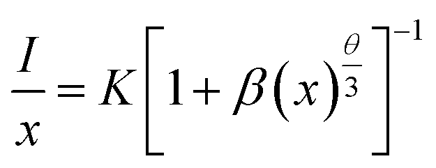
The concentration quenching mechanism is understood by obtaining the slope of log(I/x) vs. logx, where I is the PL intensity, and x is the doping concentration. The equation follows
| |
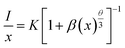 | (3) |
where
β and
θ are constants, with
θ = 6, 8, and 10 for the mechanisms dipole–dipole, dipole–quadrapole and quadrapole–quadrapole. From
Fig. 4g, the slope is nearly 3, indicating the non-radiative energy transfer among adjacent Mn
2+ ions.
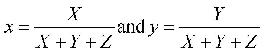
In the present study, diodes were fabricated by depositing Mg–Mn doped ZnO on p-Si, with color coordinates (0.383, 0.368) to (0.457–0.391). The color parameters were determined to get an insight into the possible color application of the diode. Emitted colors from the samples are plotted (x, y) in the CIE color space as shown in Fig. 4h. This CIE color space is used to calculate color parameters like dominant wavelength, luminous efficiency, correlated color temperature (CCT) (Fig. 4i). Linearity of color space X, Y, Z are given by
| |
 | (4) |
For constant k > 0, the spectral distribution of the given color is represented by P(λ). ![[x with combining macron]](https://www.rsc.org/images/entities/i_char_0078_0304.gif) (λ), ȳ(λ), and
(λ), ȳ(λ), and ![[z with combining macron]](https://www.rsc.org/images/entities/i_char_007a_0304.gif) (λ) show the number of primaries X, Y, and Z that match the color wavelength (λ) of the visible spectrum. Colorimetric (x, y) coordinates defined by normalized against X + Y + Z as
(λ) show the number of primaries X, Y, and Z that match the color wavelength (λ) of the visible spectrum. Colorimetric (x, y) coordinates defined by normalized against X + Y + Z as
| |
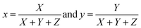 | (5) |
The obtained (x, y) values for various samples are listed in Table 4.
Table 4 Emission parameters obtained from PL data for (Mn,Mg):ZnO thin films
| Sample |
(x, y) |
CCT (K) |
| S0 |
(0.403, 0.381) |
3478 |
| S1 |
(0.457, 0.391) |
2576 |
| S2 |
(0.393, 0.367) |
3604 |
| S3 |
(0.383, 0.365) |
3839 |
| S4 |
(0.401, 0.386) |
3558 |
The dominant wavelength will specify the wavelength the light source emits most of the time. (x, y) coordinate is a mixture of saturated light of a specific dominant wavelength and the white illuminant. A line from white illuminant is drawn through the sample's color coordinates (x, y) to connect the edge of the 1931 CIE color space. The dominant color observed is yellow (∼585 nm). Thus, the films could be used as a yellow phosphor in lighting applications.
The color of the radiated light is characterized by color temperature. The correlated color temperature given in kelvin corresponds to the color of radiation of the black body. Using Mc Cammy's formula, CCT values were calculated.
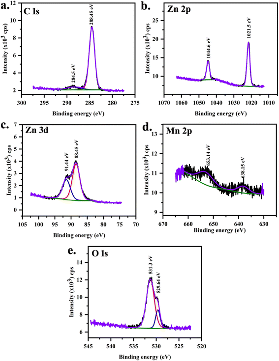
3.5 X-ray photoelectron spectroscopy
XPS was performed on MnZnO (Fig. 5) and 2 at% Mg doped MnZnO (Fig. 6) samples to investigate the chemical states of Mg, Mn, and Zn. XPS spectra were analyzed using the CASA XPS Demo version. A Tougard background subtraction which is a mixture of Gaussian and Lorentzian was used. Charge neutralization was done using the C 1s signal. Two peaks were observed corresponding to C 1s that arise from C–C or C–H and C–OH. The carbon correction is therefore done with 284.8 eV. This process of carbon correction is reported to have an error of ±0.1 eV.
 |
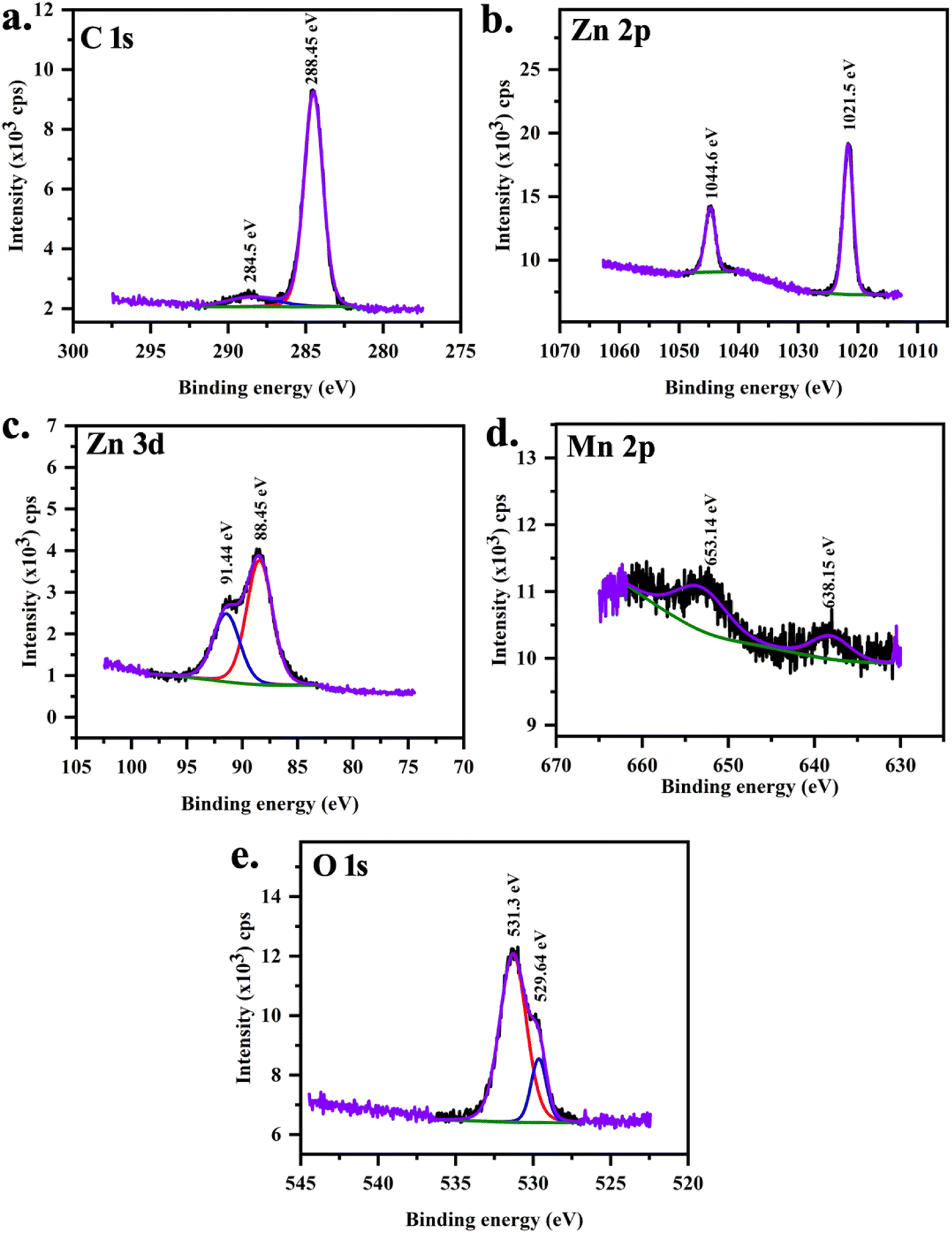
| | Fig. 5 XPS core spectra of MnZnO (S0) sample (a) C 1s, (b) Zn 2p, (c) Zn 3d, (d) Mn 2p and (e) O 1s. | |
 |
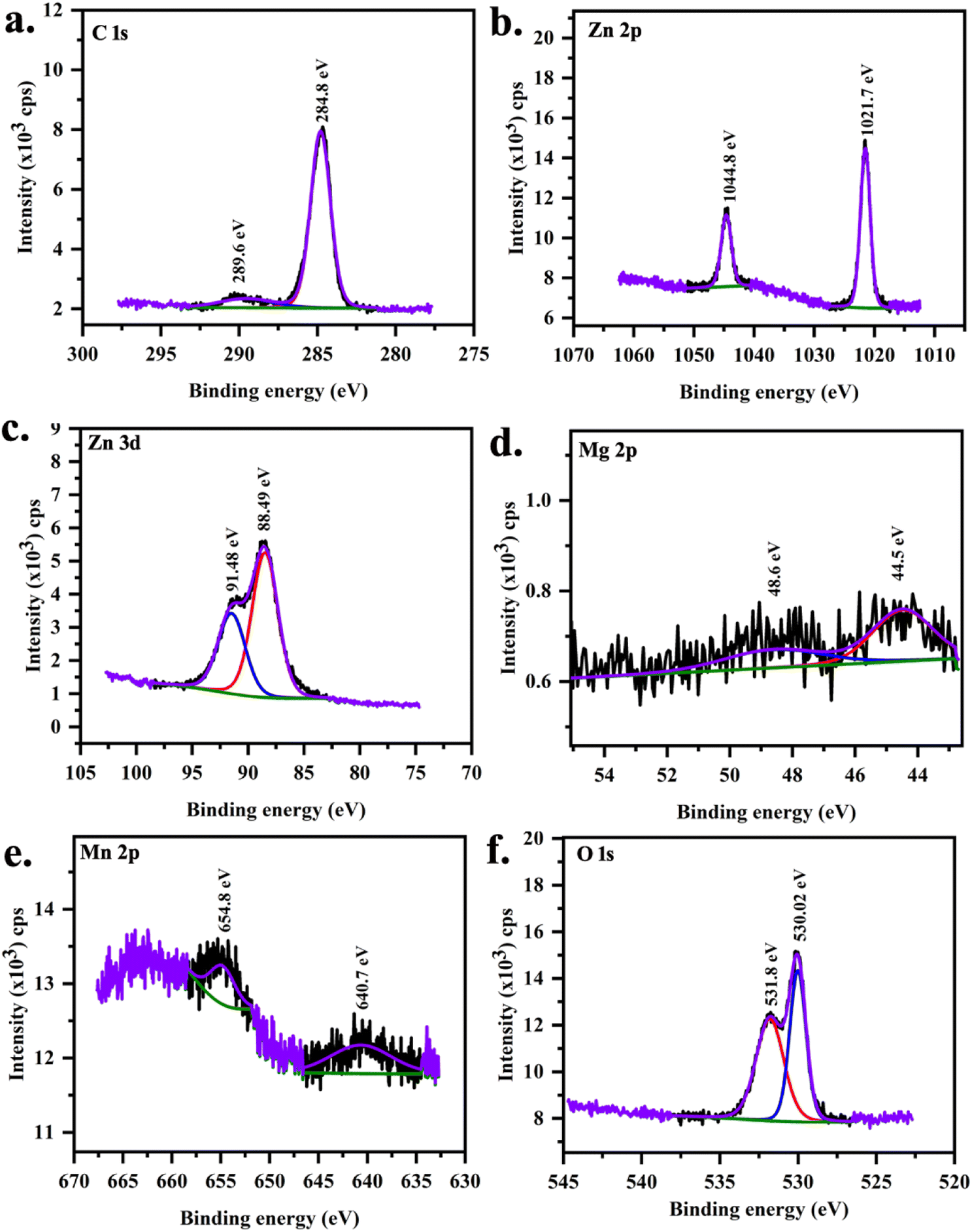
| | Fig. 6 XPS core spectra of MgMn:ZnO (S2 sample) (a) C 1s, (b) Zn 2p, (c) Zn 3d, (d) Mg 2p, (e) Mn 2p and (f) O 1s. | |
XPS peaks at 638.19 eV and 652.81 eV are associated with the manganese with j = 3/2 and j = 1/2 in MnZnO (Table 5). In (Mn,Mg)ZnO film, it is observed at 640.49 eV and 654.79 eV. This indicates the +2 valence state of the Mn ions in the ZnO lattice,52 as the metallic Mn peak was observed at 637.7 eV, and Mn4+ at 642.4 eV.53,54 The intensity of Mn peaks was weak, due to the low level of Mn dopant concentration. It shows that the content of Mn ions at the surface is low.55 As the intensity is low, no satellite peaks could be distinguished. FWHM and area of Mn 2p1/2 peak is more for S0 than for S2. This indicates that the Mn concentration in S0 is more than in S2. The spin–orbit splitting for S0 and S2 were 14.6 eV and 14.3 eV respectively. The area ratio of the peaks (2p1/2)/(2p3/2) in both samples was nearly 0.5, which is per the j values. Mg 2p XPS peak at 44.56 eV, and 48.76 eV ascribed to the presence of Mg2+ replacing Zn.42,56,57 Adding Mg to the MnZnO can either replace Mn or Zn or form MgO. In the case of MnZnO, Zn 2p3/2 appears at 1021.52 eV representing Zn–O bonds. With Mg doping, 2p3/2 shifted to high binding energy, i.e., 1021.66 eV (Table 6). This resulted from the replacement of Zn by Mg and Mn. This also added to Mn–Zn–O–Mg binding energy. The area under the peak for Zn core spectra was more for S2 than S0 which is in line with the higher percentage of Zn composition observed in S2 than S0 in EDX. The zinc-related XPS lines corresponding to the 2p orbit are separated by 23.1 eV in S0 and S2. These peaks were unaltered in terms of position, width, and shape. Zn 3d peaks were observed at 91.38 and 88.42 eV for j = 3/2 and 5/2 respectively. O 1s peak at 529.64 eV corresponds to O2− on the ZnO array. Higher O 1s binding energies were identified at 530.02 eV with the addition of Mg ascribed to Zn–O–Mn–Mg bonds.42 O 1s peak at higher binding energy at 531.3 eV and 531.8 eV is related to loosely bonded oxygen (adsorbed C–O/C–OH) or the chemisorbed53 observed in the core spectra of carbon.
Table 5 XPS peak fit results for S0 sample
| Element |
Core level |
Binding energy (eV) |
Spin orbit splitting |
FWHM |
Area ratio |
Assignment |
| Zn |
3d3/2 |
91.38 |
2.96 |
3.05 |
0.65 |
ZnO |
| 3d5/2 |
88.42 |
2.67 |
| 2p1/2 |
1021.52 |
23.1 |
1.90 |
0.49 |
| 2p3/2 |
1044.6 |
2.04 |
| O |
1s |
529.64 |
— |
1.17 |
— |
ZnO |
| 531.30 |
2.03 |
Mn–O |
| C |
1s |
284.50 |
— |
1.43 |
— |
— |
| 288.45 |
3.87 |
| Mn |
2p1/2 |
652.81 |
14.6 |
5.77 |
0.49 |
Mn–O |
| 2p3/2 |
638.19 |
5.21 |
Table 6 XPS peak fit details for S2 sample
| Element |
Core level |
Binding energy (eV) |
Spin orbit splitting |
FWHM |
Area ratio |
Assignment |
| Mg |
2p1/2 |
48.76 |
4.19 |
3.22 |
0.50 |
Mg–O |
| 2p3/2 |
44.57 |
3.13 |
| Zn |
3d3/2 |
91.39 |
2.93 |
3.02 |
0.67 |
ZnO |
| 3d5/2 |
88.46 |
2.58 |
| 2p1/2 |
1021.66 |
23.12 |
1.95 |
0.48 |
| 2p3/2 |
1044.78 |
2.10 |
| O |
1s |
530.02 |
— |
1.23 |
— |
ZnO |
| 531.8 |
2.10 |
Mn–O |
| C |
1s |
284.79 |
— |
1.49 |
— |
— |
| 289.56 |
4.09 |
| Mn |
2p1/2 |
654.79 |
14.3 |
2.39 |
0.51 |
Mn–O |
| 2p3/2 |
640.49 |
7.30 |
3.6 Electrical properties of (Mn,Mg)ZnO/p-Si heterojunctions
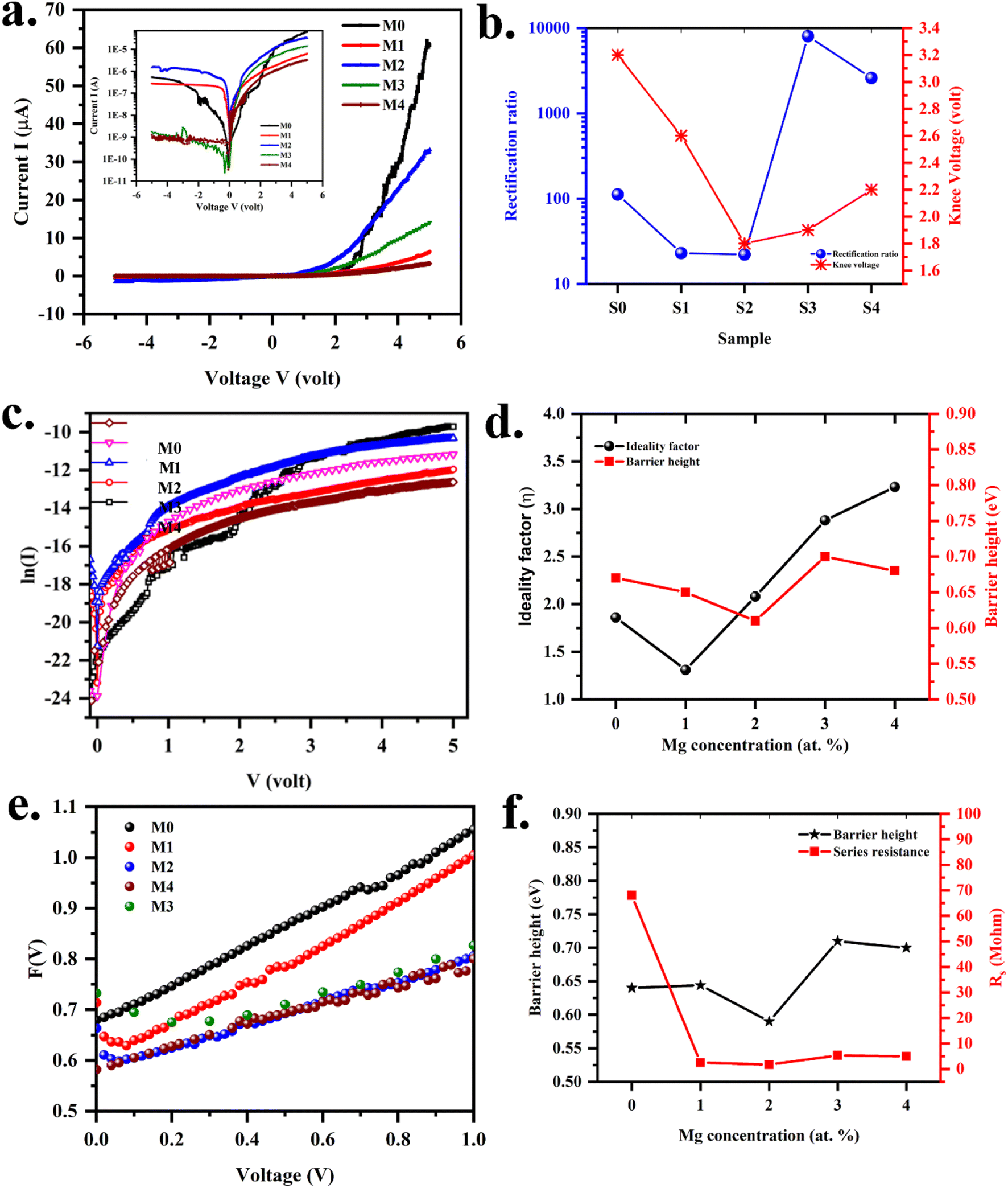
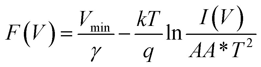
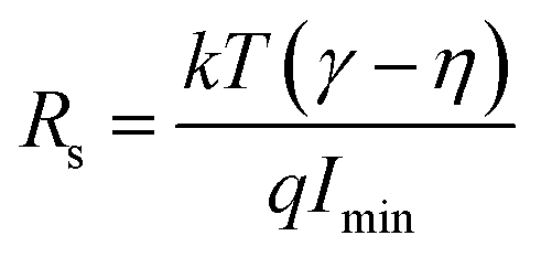
The illustration of the energy band diagram according to Anderson's model is built and is depicted in Fig. 7. Band gaps of ZnO and Si are taken as Eg(ZnO) = 3.3 eV, Eg(Si) = 1.12 eV.58,59 The electron affinity of ZnO χZnO = 4.35 eV, and that of Si, χSi = 4.05 eV. The observed conduction band offset, ΔEc was only 0.3 eV, and the valence band offset nearly 2.55 eV which is well suited for diode fabrications.58–61 When the device is operated in the reverse bias regime, the depletion width of ZnO increases larger than the depletion width in p-Si. Electron–hole pairs will be created by band-to-band tunnelling in this depletion layer by a high electric field. Electrons and holes accelerate in the opposite direction and get sufficient energy to excite Mn and Mg ions by ionization. I–V measurements are used to reveal the characteristic diode parameters. The I–V characteristics for (Mn,Mg):ZnO/p-Si at room temperature are shown in Fig. 8a. Fabricated diodes show p–n junction confirmation by the nonlinear I–V characteristics. Heterostructures show a rectifying diode characteristic with turn on voltage within 3 V and with low leakage current for all samples (Fig. 8b). From the Schottky–Mott model, assuming that the current transport mechanism is controlled by the thermionic emission process, the forward current is given by eqn (6). A voltage vs. ln(I) plot was drawn (Fig. 8c). The behavior of the forward I–V curve can be divided into three parts according to the power law (in log–log I–V curve, not shown here), wherein below 1 V, a linear behavior of current with voltage was observed which is due to the dominant tunnelling mechanism. From 1 V to 3 V, an exponential increase in current was observed due to the tunnelling by recombination mechanism. At forward bias higher than 3 V, the nature of the I–V characteristic deviates from that of ideal thermionic behavior due to the space charge limited current conduction. The parameters like ideality factor, barrier height acquired from the slope, and intercepts of forward I–V plot in the linear region at low bias voltage. In the plot of lnI vs. V, the slope = q/ηkT, and saturation current I0 is got by the exponential of intercept, which is substituted in eqn (8) to obtain barrier height. From the model, current,| |
 | (6) |
I0 was obtained from the intercept of ln(I) vs. V at V = 0.| |
 | (7) |
| |
 | (8) |
where q is the charge of the electron, V is applied bias voltage, k is the Boltzmann constant, T is temperature, A is the area of the diode (0.5 cm2), A* is the Richardson constant (32 A cm−2 K−2), Φ is the barrier height, η is the ideality factor. η exceeding unity (Fig. 8d) attributed to the native oxide layers and the high value of η confirms the non-ideal behavior of diode, due to series resistance and interface layer. It could be seen that as the ideality factor increased for M4, the barrier height decreased. When η is higher than 1, the diode is moving away from the ideality, and the thermionic emission is accompanied by other transport mechanism. In present samples, the ideality factor higher than one, indicates additional contribution for the transport properties from the interface states, barrier inhomogeneity, surface oxide on Si, image-force effect, series resistance, the tunnelling process, and non-uniformly distributed interfacial charges. For samples M3, and M4, the ideality factors are 2.88 and 3.23 respectively indicating the dominant generation-recombination mechanism in the space charge region.
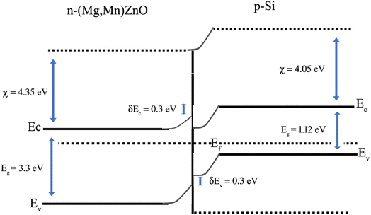 |
| | Fig. 7 Anderson's model for the band alignment of ZnO/p-Si heterojunction. | |
 |
| | Fig. 8 (a) Current vs. voltage curve (inset: log scale) (b) rectification and knee voltage (c) plot of voltage vs. lnI TE model (d) variation of ideality factor and barrier height (e) plot of F(V) vs. voltage (f) variation of ideality factor and series resistance Norde model for (Mn,Mg)ZnO/p-Si heterojunctions. | |
Further to determine the series resistance, Norde model was employed. Norde function is given by
| |
 | (9) |
| |
 | (10) |
| |
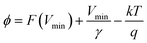 | (11) |
where
γ is an integer immediately next higher than the ideality factor obtained from the
I–
V curve.
Eqn (10) provides the series resistance and 10, the barrier height from the
F(
V)
vs. I curve (
Fig. 8e). The values obtained from Norde's model are listed in
Table 7. The values obtained from the TE model and Norde model were nearly the same. The theoretical barrier height is 0.7 eV and the experimentally observed value is in the range of 0.6–0.82 eV.
58–61 Imin is the minimum value of current corresponding to
F(
Vmin). The barrier height values varying with the Mg concentration are given in
Fig. 8e.
Table 7 Diode parameters for the samples prepared in comparison with literature
| Sample |
Ideality factor |
Barrier height (eV) |
Series resistance (M-ohm) |
| TE model |
Norde model |
| M0 |
1.86 |
0.67 |
0.64 |
68.0 |
| M1 |
1.31 |
0.65 |
0.64 |
2.5 |
| M2 |
2.08 |
0.61 |
0.59 |
1.7 |
| M3 |
2.88 |
0.70 |
0.71 |
5.3 |
| M4 |
3.23 |
0.68 |
0.70 |
5.0 |
| ZnO/p-Si62 |
1.4–2.2 |
0.62–0.72 |
0.6–0.71 |
— |
| LaZnO/p-Si60 |
2.48–2.92 |
0.63–0.68 |
0.65–0.72 |
— |
| ZnO/p-Si59 |
∼3.7 |
0.52 |
— |
— |
| n-ZnO/p-Si58 |
3.14–3.5 |
0.66–0.79 |
— |
— |
4 Conclusion
XRD indicates phase pure dual doped (Mn,Mg)ZnO without any secondary impurity phases related to the dopants Mn, Mg. SEM showed uniformly deposited films. EDX showed a precision of the added and observed elemental composition. Exchange constant indicating s-states found to reduce the CB and p-states found to rise the top level of VB that changed the band gaps with the Mg dopant level. Defect levels of Mn and Mg are observed in the samples. A dominant wavelength of 585 nm corresponding to yellow color was observed as suitable for yellow LED. Raman spectra showed LO mode and multiphonon scattering from sp–d interaction at oxygen vacancy. Raman line shifts and widths indicated the defects in the sample. Formed ZnMnMgO/p-Si diodes showed low threshold voltage for 2 at% Mg doped MnZnO along with low leakage current suitable for LED. XPS showed doping of Mn2+ and Mg2+ on to the Zn2+ sites of the ZnO system. Further detailed study on the fabrication of LEDs using the (Mn,Mg)ZnO thin films is needed to understand the efficiency of the formed LED.
Conflicts of interest
The authors declare that they have no conflict of interest.
Acknowledgements
Ganesha Krishna V. S. is thankful to DST India for providing INSPIRE fellowship under grant number IF190268.
References
- D. J. Qiu, H. Z. Wu, A. M. Feng, Y. F. Lao, N. B. Chen and T. N. Xu, Annealing effects on the microstructure and photoluminescence properties of Ni-doped ZnO films, Appl. Surf. Sci., 2004, 222, 263–268, DOI:10.1016/j.apsusc.2003.08.015.
- F. Wang and C. Chang, Effect of substrate temperature on transparent conducting Al and F co-doped ZnO thin films prepared by rf magnetron sputtering, Appl. Surf. Sci., 2016, 370, 83–91, DOI:10.1016/j.apsusc.2016.02.161.
- Y. Vijayakumar, P. Nagaraju, V. Yaragani, S. R. Parne, N. S. Awwad and M. V. Ramana Reddy, Nanostructured Al and Fe co-doped ZnO thin films for enhanced ammonia detection, Phys. B: Condens. Matter., 2020, 581, 411976, DOI:10.1016/j.physb.2019.411976.
- J. Chen, D. Chen, J. He, S. Zhang and Z. Chen, The microstructure, optical, and electrical properties of sol–gel-derived Sc-doped and Al–Sc co-doped ZnO thin films, Appl. Surf. Sci., 2009, 255(23), 9413–9419, DOI:10.1016/j.apsusc.2009.07.044.
- R. Ebrahimifard, M. R. Golobostanfard and H. Abdizadeh, Sol–gel derived Al and Ga co-doped ZnO thin films: An optoelectronic study, Appl. Surf. Sci., 2014, 290, 252–259, DOI:10.1016/j.apsusc.2013.11.062.
- A. K. Abduev, A. K. Akhmedov and A. S. Asvarov, The structural and electrical properties of Ga-doped ZnO and Ga, B-codoped ZnO thin films: the effects of additional boron impurity, Sol. Energy Mater. Sol. Cells, 2007, 91(4), 258–260, DOI:10.1016/j.solmat.2006.09.008.
- A. Goktas, F. Aslan, B. Yeşilata and İ. Boz, Physical properties of solution processable n-type Fe and Al co-doped ZnO nanostructured thin films: role of Al doping levels and annealing, Mater. Sci. Semicond. Process., 2018, 75, 221–233, DOI:10.1016/j.mssp.2017.11.033.
- M. N. Huda Liton, A. K. Mohammad Farid Ul Islam, M. Kamruzzaman, M. K. Rahman Khan, M. Al Helal and M. M. Rahman, Dual acceptor (N, Cu) doping effects on the electronic and optical properties of ZnO, Mater. Chem. Phys., 2020, 242, 122463, DOI:10.1016/j.matchemphys.2019.122463.
- L. Duan, et al., Annealing effects on properties of Ag–N dual-doped ZnO films, Appl. Surf. Sci., 2012, 258(24), 10064–10067, DOI:10.1016/j.apsusc.2012.06.075.
- G. Zheng, et al., Investigation of physical properties of F-and-Ga co-doped ZnO thin films grown by RF magnetron sputtering for perovskite solar cells applications, Mater. Sci. Semicond. Process., 2020, 112, 105016, DOI:10.1016/j.mssp.2020.105016.
- Z. Gu, et al., Optical properties of (Mn, Co) co-doped ZnO films prepared by dual-radio frequency magnetron sputtering, Thin Solid Films, 2006, 515(4), 2361–2365, DOI:10.1016/j.tsf.2006.04.030.
- X. Q. Gu, L. P. Zhu, Z. Z. Ye, H. P. He, Y. Z. Zhang and B. H. Zhao, Preparation of Li and Er codoped ZnO thin films and their photoluminescence, Thin Solid Films, 2009, 517(17), 5134–5136, DOI:10.1016/j.tsf.2009.03.004.
- J. G. Lu, Z. Z. Ye, F. Zhuge, Y. J. Zeng, B. H. Zhao and L. P. Zhu, p-type conduction in N–Al co-doped ZnO thin films, Appl. Phys. Lett., 2004, 85(15), 3134–3135, DOI:10.1063/1.1803935.
- L. El Mir, Z. Ben Ayadi, M. Saadoun, K. Djessas, H. J. von Bardeleben and S. Alaya, Preparation and characterization of n-type conductive (Al, Co) co-doped ZnO thin films deposited by sputtering from aerogel nanopowders, Appl. Surf. Sci., 2007, 254(2), 570–573, DOI:10.1016/j.apsusc.2007.06.028.
- D. Chakraborti, S. Ramachandran, G. Trichy, J. Narayan and J. T. Prater, Magnetic, electrical, and microstructural characterization of ZnO thin films codoped with Co and Cu, J. Appl. Phys., 2007, 101(5), 053918, DOI:10.1063/1.2711082.
- L. L. Chen, et al., p-type behavior in In–N codoped ZnO thin films, Appl. Phys. Lett., 2005, 87(25), 252106, DOI:10.1063/1.2146309.
- J.-S. Xie and Q. Chen, Li–N dual-doped ZnO thin films prepared by an ion beam enhanced
deposition method, Chin. Phys. B, 2014, 23(9), 097703, DOI:10.1088/1674-1056/23/9/097703.
- L. Duan, et al., The synthesis and characterization of Ag–N dual-doped p-type ZnO: experiment and theory, Phys. Chem. Chem. Phys., 2014, 16(9), 4092, 10.1039/c3cp53067a.
- M. A. M. Ahmed, W. E. Meyer and J. M. Nel, Effect of (Ce, Al) co-doped ZnO thin films on the Schottky diode properties fabricated using the sol-gel spin coating, Mater. Sci. Semicond. Process., 2019, 103, 104612, DOI:10.1016/j.mssp.2019.104612.
- D. K. Hwang, et al., P-ZnO/n-GaN heterostructure ZnO light-emitting diodes, Appl. Phys. Lett., 2005, 86(22), 1–3, DOI:10.1063/1.1940736.
- N. H. Alvi, K. ul Hasan, O. Nur and M. Willander, The origin of the red emission in n-ZnO nanotubes/p-GaN white light emitting diodes, Nanoscale Res. Lett., 2011, 6(1), 1–7, DOI:10.1186/1556-276X-6-130.
- R.-H. Horng, K.-C. Shen, C.-Y. Yin, C.-Y. Huang and D.-S. Wuu, High performance of Ga-doped ZnO transparent conductive layers using MOCVD for GaN LED applications, Opt. Express, 2013, 21(12), 14452, DOI:10.1364/oe.21.014452.
- Q. Shi, et al., Single-phased emission-tunable Mg and Ce co-doped ZnO quantum dots for white LEDs, Spectrochim. Acta, Part A, 2020, 231, 118096, DOI:10.1016/j.saa.2020.118096.
- X. Ma and Z. Wang, Microelectronic Engineering The UV and blue light emission properties of Mn doped ZnO nanocrystals, Microelectron. Eng., 2011, 88(10), 3168–3171, DOI:10.1016/j.mee.2011.06.021.
- X. Li, X. Zhu and K. Jin, Study on structural and optical properties of Mn-doped ZnO thin films by sol-gel method, Opt. Mater., 2020, 100, 1–7, DOI:10.1016/j.optmat.2020.109657.
- T. Pasang and K. Namratha, Synthesis, characterization and properties of Mn-doped ZnO nanocrystals, Adv. Nat. Sci.: Nanosci. Nanotechnol., 2012, 3, 5pp, DOI:10.1088/2043-6262/3/3/035005.
- L. Wang, et al., Mg-Doped ZnO Nanoparticle Films as the Interlayer between the ZnO Electron Transport Layer and In P Quantum Dot Layer for Light-Emitting Diodes, J. Phys. Chem. C, 2020, 124, 8758–8765, DOI:10.1021/acs.jpcc.0c00351.
- F. K. Shan, et al., Blueshift of near band edge emission in Mg doped ZnO thin films and aging, J. Appl. Phys., 2004, 95(9), 4772–4776, DOI:10.1063/1.1690091.
- S. A. Azzez, Z. Hassan, J. J. Hassan, M. S. Mukhlif, M. S. Mahdi and M. Bououdina, Effect of temperature on hydrothermally grown high-quality single-crystals Mg-doped ZnO nanorods for light-emitting diode application, J. Lumin., 2017, 192, 634–643, DOI:10.1016/j.jlumin.2017.07.050.
- Y. H. Mohammed, Superlattices and microstructures fabrication of n-MgZnO/p-Si heterojunction diode: role of magnesium doping, Superlattices Microstruct., 2019, 131, 104–116, DOI:10.1016/j.spmi.2019.06.001.
- S. AKSOY, Fabrication of n-ZnO:Mn/p-Si heterojunction diodes and its I–V, C–V characteristics, Tech. Univ. J. Sci. Technol. A – Appl. Sci. Eng., 2019, 20(3), 296–306, DOI:10.18038/estubtda.506606.
- K. M. Sandeep, S. Bhat and S. M. Dharmaprakash, Structural, optical, and LED characteristics of ZnO and Al doped ZnO thin films, J. Phys. Chem. Solids, 2017, 104, 36–44, DOI:10.1016/j.jpcs.2017.01.003.
- S. Chawla and H. Chander, Enhancement of luminescence in ZnMgO thin-film nanophosphors and applications and materials science, Int. Congr. Adv. Appl. Phys. Mater. Sci., 2008, 274(2), 271–274, DOI:10.1002/pssa.200723149.
- V. S. Ganesha Krishna and M. G. Mahesha, Absence of Mn emission in MnxZn(1-x)S thin films grown by spray pyrolysis technique, J. Lumin., 2020, 230, 117716, DOI:10.1016/j.jlumin.2020.117716.
- D. Fang, C. Li, N. Wang, P. Li and P. Yao, Structural and optical properties of Mg-doped ZnO thin films prepared by a modified Pechini method, Cryst. Res. Technol., 2013, 48(5), 265–272, DOI:10.1002/crat.201200437.
- A. K. Assaifan, et al., Nanotextured Surface on Flexographic Printed ZnO Thin Films for Low Cost Non-Faradaic Biosensors, ACS Appl. Mater. Interfaces., 2016, 8(49), 33802–33810, DOI:10.1021/acsami.6b11640.
- W. Lee, et al., Investigation of electronic and
optical properties in Al–Ga codoped ZnO thin films, Curr. Appl. Phys., 2012, 12(3), 628–631, DOI:10.1016/j.cap.2011.09.008.
- S. B. Jambure, S. J. Patil, A. R. Deshpande and C. D. Lokhande, A comparative study of physico-chemical properties of CBD and SILAR grown ZnO thin films, Mater. Res. Bull., 2014, 49(1), 420–425, DOI:10.1016/j.materresbull.2013.09.007.
- L. Znaidi, T. Touam, D. Vrel, N. Souded, S. Ben Yahia and O. Brinza, ZnO Thin Films Synthesized by Sol–Gel Process for Photonic Applications, Acta Phys. Pol., A, 2012, 121(1), 165–168 CrossRef CAS.
- V. S. Ganesha Krishna and M. G. Mahesha, Spectroscopic, and electrical properties of Cu:ZnO thin films, J. Alloys Compd., 2022, 899, 163357, DOI:10.1016/j.jallcom.2021.163357.
- A. Mathur, P. Halappa and C. Shivakumara, Synthesis and characterization of – Sm3+ activated LaGdPO phosphors for white LEDs applications, J. Mater. Sci.: Mater. Electron., 2018, 29(23), 19951–19964, DOI:10.1007/s10854-018-0125-7.
- V. Etacheri, R. Roshan and V. Kumar, Mg-Doped ZnO Nanoparticles for Efficient Sunlight-Driven Photocatalysis, ACS Appl. Mater. Interfaces, 2012, 4(5), 2717–2725, DOI:10.1021/am300359h.
- D. N. Montenegro, et al., Non-radiative recombination centres in catalyst-free ZnO nanorods grown by atmospheric-metal organic chemical vapour deposition, J. Phys. D Appl. Phys., 2013, 46(23), 235302, DOI:10.1088/0022-3727/46/23/235302.
- A. K. Singh, G. S. Thool and P. R. Bangal, Low temperature Mn doped ZnO nanorod array: synthesis and its photoluminescence behavior, Ind. Eng. Chem. Res., 2014, 53(22), 9383–9390 CrossRef CAS.
- D. Fang, P. Yao and H. Li, Influence of annealing temperature on the structural and optical properties of Mg–Al co-doped ZnO thin films prepared via sol–gel method, Ceram. Int., 2014, 40(4), 5873–5880, DOI:10.1016/j.ceramint.2013.11.030.
- E. Manikandan, V. Murugan, G. Kavitha, P. Babu and M. Maaza, Nanoflower rod wire-like structures of dual metal (Al and Cr) doped ZnO thin films: structural, optical and electronic properties, Mater. Lett., 2014, 131, 225–228, DOI:10.1016/j.matlet.2014.06.008.
- N. Fadilah, N. Badar and R. Rusdi, Optical Band Gap Energies of Magnesium Oxide (MgO) Thin Film and Spherical Nanostructures, in International Congress on Advances in Applied Physics and Materials Science, 2011, pp. 328–332, DOI:10.1063/1.3663137.
- R. Viswanatha, et al., Synthesis and Characterization of Mn-Doped ZnO Nanocrystals, J. Phys. Chem. B, 2004, 108(20), 6303–6310, DOI:10.1021/jp049960o.
- J. B. Coulter, D. P. Birnie and D. P. B. Iii, Assessing Tauc Plot Slope Quantification: ZnO Thin Films as a Model System, Phys. Status Solidi B, 2018, 255(3), 1–7, DOI:10.1002/pssb.201700393.
- B. Lin, Z. Fu and Y. Jia, Green luminescent center in undoped zinc oxide films deposited on silicon substrates, Appl. Phys. Lett., 2001, 79(7), 943–945, DOI:10.1063/1.1394173.
- C. H. Ahn, Y. Y. Kim, D. C. Kim, S. K. Mohanta and H. K. Cho, A comparative analysis of deep level emission in ZnO layers deposited by various methods, J. Appl. Phys., 2009, 105(1), 013502, DOI:10.1063/1.3054175.
- R. Ponnusamy, S. C. Selvaraj, M. Ramachandran, P. Murugan, P. M. G. Nambissan and D. Sivasubramanian, Diverse Spectroscopic Studies and First-Principles Investigations of the Zinc Vacancy Mediated Ferromagnetism in Mn-Doped ZnO Nanoparticles, Cryst. Growth Des., 2016, 16(7), 3656–3668, DOI:10.1021/acs.cgd.6b00110.
- H. Y. Xu, Y. C. Liu, C. S. Xu, Y. X. Liu, C. L. Shao and R. Mu, Room-temperature ferromagnetism in (Mn, N)-codoped ZnO thin films prepared by reactive magnetron cosputtering, Appl. Phys. Lett., 2006, 88(24), 242502, DOI:10.1063/1.2213929.
- V. S. Ganesha Krishna and M. G. Mahesha, Assessment of the anharmonic phonon decay, Fröhlich interactions, and phonon lifetime in Zn 0.98 Mn 0.02 S thin films through temperature-dependent Raman spectroscopy, J. Raman Spectrosc., 2023, 54(4), 446–452, DOI:10.1002/jrs.6498.
- O. D. Jayakumar, C. Sudakar, A. Vinu, A. Asthana and A. K. Tyagi, Effect of Surfactant Treatment on the Magnetic Properties of Mn-Doped ZnO Bulk and Nanoparticles, J. Phys. Chem. C, 2009, 113(12), 4814–4819, DOI:10.1021/jp809288s.
- V. S. Ganesha Krishna and M. G. Mahesha, Analysis of surface properties of Mg doped ZnS and ZnSe thin films through X-ray photoelectron spectroscopy, J. Electron Spectrosc. Relat. Phenom., 2023, 266, 147341, DOI:10.1016/j.elspec.2023.147341.
- V. S. Ganesha Krishna and M. G. Mahesha, spectroscopic valuation of phonon lifetime and surface characteristics of ZnMgS thin film, J. Chem. Phys., 2022, 157, 014703 CrossRef PubMed.
- S. Sharma and C. Periaswamy, A study on the electrical characteristic of n-ZnO/p-Si heterojunction diode prepared by vacuum coating technique, Superlattices Microstruct., 2014, 73, 12–21 CrossRef CAS.
- V. Quemener, M. Alnes, L. Vines and P. Rauwel, The work function of n-ZnO deduced from heterojunctions with Si prepared by ALD, J. Phys. D Appl. Phys., 2012, 45, 5pp CrossRef.
- G. I. Buyuk and I. Saliha, Electrical and photovoltaic properties of p–n heterojunctions obtained using sol gel derived nanostructured ZnO:La films onto p-Si, Superlattices Microstruct., 2020, 145, 106605 CrossRef CAS.
- W. Chebil, A. Gokarna and N. Fouzri, Study of the growth time effect on the structural, morphological and electrical characteristics of ZnO/p-Si heterojunctions bu sol gel assisted chemical bath deposition, J. Alloys Compd., 2018, 779, 448–455, DOI:10.1016/j.jallcom.2018.08.280.
- N. K. Das, Electrical Properties of CSS Deposited CdTe Thin Films for Solar Cell Applications, in 2019 1st Int. Conf. Adv. Sci. Eng. Robot. Technol., 2019, pp. 1–4 Search PubMed.
|
| This journal is © The Royal Society of Chemistry 2023 |
Click here to see how this site uses Cookies. View our privacy policy here. 
 Open Access Article
 This Open Access Article is licensed under a Creative Commons Attribution-Non Commercial 3.0 Unported Licence
 *
*