
 Open Access Article
 This Open Access Article is licensed under a Creative Commons Attribution-Non Commercial 3.0 Unported Licence
Quantitative nanoscale temperature mapping across the multi-quantum well of a light-emitting diode in operation using vacuum null-point scanning thermal microscopy to evaluate local energy conversion efficiency
Hwijong Shin†
,
Seosi Liu† and
Ohmyoung Kwon *
*
School of Mechanical Engineering, Korea University, Seoul 136-701, South Korea. E-mail: omkwon@korea.ac.kr
First published on 23rd November 2023
Abstract
Electrical energy that is not converted into light in light emitting diodes (LEDs) is locally dissipated as heat in the active layers. Therefore, by measuring the temperature distribution with nanoscale resolution across the multi-quantum well (MQW) of an LED in operation, the effect of nanostructures inside the LED on the local energy conversion efficiency can be observed. In this study, we first demonstrated that vacuum null-point scanning thermal microscopy (VNP SThM) could be used to quantitatively map the two-dimensional temperature distribution across the MQW of an LED in operation with a sufficient signal-to-noise ratio. Subsequently, by increasing the injection current in four steps, we quantitatively mapped the temperature distribution across the MQW at each step and observed the shift in the temperature peak across the active layers due to the increase in injection current. The measurements of the temperature distribution around the MQW indicate that as the injection current increased, the overall temperature around the MQW increased significantly, and the temperature peak position shifted. These results show that the main cause of the dissipation of electrical energy into thermal energy inside an LED changes as the injection current increases, and the nanostructures inside an LED affect the dissipation of electrical energy into thermal energy. The high thermal sensitivity, nanoscale resolution, and convenience of VNP SThM may enable the direct observation of the effect of the nanostructures inside various types of nanophotonic devices on local energy conversion even under intense localized radiation.
Introduction
Light-emitting diodes (LEDs) are energy conversion devices that convert electrical energy into light. LEDs are rapidly replacing existing light-emitting devices because of their high energy efficiency, long lifespan, and low-cost mass production. For example, gallium nitride (GaN)-based LEDs are used in a wide range of applications such as liquid crystal display backlights, large screen displays, and general lighting.1–3 In addition, AlGaN LEDs can be tuned to cover nearly the entire ultraviolet spectral range (210–400 nm), making them well suited for applications across various fields, including the biological, environmental, industrial, and medical fields.4 In addition, mini-LEDs and micro-LEDs are considered the most promising next-generation display technologies.5,6In the research and development on LEDs, efficiency improvement is very important, particularly at high current densities. Current commercial LEDs exhibit considerably high efficiencies; however, the efficiency decreases as the injection current increases.7–9 The main causes of efficiency droop are Auger recombination in the quantum-well region10–13 and electron leakage into the p-doped region.14–18 However, the causes of efficiency droop in various types of LEDs are being investigated.19–21
To date, most studies have analyzed the cause of efficiency droop based on modeling or by measuring the light output outside the LED chip and analyzing the luminous efficiency, light intensity, and wavelength. Although various theoretical models have been developed, uncertainties still exist regarding the leakage currents and material properties used for modeling.
For example, in the case of electroluminescence measurements, arbitrary assumptions about the current-injection efficiency are necessary.22,23 Problems are also associated with photoluminescence owing to the change in energy bands according to bias and the correspondence between the excitation power for photoluminescence and current injection for electroluminescence.19 Experimental Auger electron measurements showed that the appearance of Auger electron peaks coincided with the efficiency droop.12,13 However, the Auger electron measurement does not exclude all other factors that may lead to an efficiency droop in LEDs, and it is still only an indirect tool for the analysis of other factors.
In LEDs, electrical energy that is not converted into light in the active layers dissipates locally as heat. Therefore, the direct measurement of the temperature distribution around the multi-quantum well (MQW) in an operating LED enables the direct evaluation of the local energy conversion efficiency of the LED. However, as mentioned previously, few of the measurement studies conducted to date have performed local and direct measurements of the energy conversion phenomenon (from electricity to light or heat) occurring in LEDs. Direct and local measurements of the energy conversion phenomenon are required for a more reliable and simple analysis of the efficiency droop phenomenon.
Because the thickness of each layer of the MQW and surrounding epilayers is less than 100 nm, a temperature measurement tool with nanoscale spatial resolution is required. However, quantitatively measuring the temperature distribution around the MQW on the cross section of an operating LED with a spatial resolution of several nanometers corresponding to the characteristic length of the nanostructures constituting the epilayers is challenging. At present, scanning thermal microscopy (SThM), which is one of the few temperature measurement tools with a nanoscale resolution (∼10 nm), seems to be the most suitable tool for measuring the temperature distribution around the MQW on the cross section of an LED in operation.24
However, conventional SThM, which determines temperature/thermal properties by scanning the surface of the sample with an SThM probe in air, cannot be used to map the temperature locally and quantitatively because of the following three limitations: (i) heat transfer between the probe and sample through air, (ii) change in the contact thermal resistance between the probe tip and sample surface, and (iii) temperature perturbation of the sample due to heat flux transferred through the tip-sample contact.25 To overcome all three limitations of conventional SThM, Chung et al. theoretically proved and developed null-point scanning thermal microscopy (NP SThM), which can quantitatively measure local temperature distribution, and experimentally demonstrated its effectiveness.26
However, in the case of an LED in operation, quantitatively measuring the local temperature across the MQW is difficult because heat is transferred not only through air but also via the intense light emitted from the MQW. Jung et al. theoretically explained that NP SThM is effective when additional heat transfer occurs via light, and they quantitatively measured the temperature distribution across the MQW on the cross section of an operating LED using NP SThM under atmospheric conditions.27
NP SThM is theoretically ideal in that it can overcome all three abovementioned limitations; however, implementing it under atmospheric conditions is cumbersome and affords low measurement sensitivity. Under ambient conditions, NP SThM requires six scans of the same scan line with the SThM probe operating in passive and active modes, and the distance between the probe tip and the sample changed scan by scan. For local measurement, it is necessary to quantitatively measure the local temperature of a sample from only an extremely small heat flux passing through the nanosized contact formed between the tip of the probe and the sample. However, under ambient conditions, sufficiently increasing the thermal sensitivity of SThM probes is difficult owing to heat transfer through air.
The results of Jung et al., who measured the temperature distribution across the MQW on the cross section of an operating LED using NP SThM under atmospheric conditions, indicate that the signal-to-noise ratio was not sufficiently high to obtain reliable measurements.27 The temperature distribution measured by Jung et al. had a measurement noise of 0.2–0.5 °C; however, the height of the temperature peak measured across the active layers was only 0.6–0.8 °C. In addition, owing to the complexity of the measurement method that entailed scanning the same scan line six times, Jung et al. obtained only one-dimensional temperature profiles but not two-dimensional temperature distributions.
Cha et al. recently analyzed the measurement characteristics of an SThM probe in vacuum and demonstrated that NP SThM can be implemented with two scans of the same scan line, even at a low vacuum (10−1 Torr or higher).28 Therefore, two-dimensional imaging with NP SThM is possible in a vacuum. More importantly, this shows that vacuum NP SThM (VNP SThM) can improve the thermal sensitivity of the measurement by at least 10 times compared with atmospheric NP SThM, even at a relatively low degree of vacuum.
In this study, we first demonstrated that VNP SThM could be implemented with two scans, even when heat transfer occurs via intense light emitted locally from the MQW of an operating LED. After validating VNP SThM in the presence of intense localized light emission, we obtained a two-dimensional temperature distribution across the MQW of an LED operating at each of the four injection current densities. In contrast to NP SThM in air, VNP SThM measures the temperature distribution with more than 10 times higher thermal sensitivity and signal-to-noise ratio, enabling a reliable analysis of the effect of LED epilayer nanostructures on local energy conversion efficiency.
Methods
NP SThM measures the temperature of the sample when the temperatures of the probe tip and sample equalize and the heat flux between them disappears, enabling measurement of unperturbed temperature. If the temperatures of the tip of the SThM probe and that of the sample surface are the same, the temperature jump Tj (≡Tc − Tnc) that occurs when the tip of the probe touches the sample surface becomes zero. Using this principle, in a previous study, Chung et al. rigorously derived the principal equation of NP SThM,26 as follows:
 | (1) |
However, as mentioned previously and detailed by Cha et al., six scans are required to obtain Ts(x) using eqn (1) under ambient conditions.28 According to eqn (1), a total of 4 scans (Tc1(x), Tc2(x), Tnc1(x), and Tnc2(x)) looks needed to calculate Ts(x). However, because two scans are required to obtain Tnc1(x), and Tnc2(x) under ambient conditions, respectively, a total of 6 scans are required to obtain Ts(x). To obtain Tnc(x) under atmospheric conditions, we determined Tl(x) at h1 and Tl(x) at h2. Tl(x) at h is the temperature profile obtained by scanning the SThM probe along the same scan line as in the contact mode but at a height h above the sample surface, using the topography data obtained in the contact mode. The subscript l indicates that the tip of the probe was lifted off the sample surface. Subsequently, for every x, by linearly extrapolating Tl(x) at h1 and Tl(x) at h2 with respect to h, we obtain Tl(x) at h = 0, which corresponds to Tnc(x), as clearly demonstrated by Kim et al.32
The 6 scans required to obtain Ts(x) under ambient conditions using eqn (1) can be performed in the following order: Typically, scan SThM probe in contact mode without intentionally heating the probe and obtain Tc1(x). Scan the SThM probe along the same scan line as in the contact mode but at a height h1 above the sample surface, using the topography data obtained in the contact mode and obtain Tl1(x) at h1. Scan the SThM probe along the same scan line as in the contact mode but at a height h2 above the sample surface, using the topography data obtained in the contact mode and obtain Tl1(x) at h2. Heat the SThM probe to a different degree. Scan SThM probe in contact mode and obtain Tc2(x). Scan the SThM probe along the same scan line as in the contact mode but at a height h1 above the sample surface, using the topography data obtained in the contact mode and obtain Tl2(x) at h1. Scan the SThM probe along the same scan line as in the contact mode but at a height h2 above the sample surface, using the topography data obtained in the contact mode and obtain Tl2(x) at h2.
Recently, Cha et al. experimentally demonstrated that Ts(x) can be obtained using eqn (1) with only two scans even at a fairly low vacuum (∼10−1 Torr).28 Even at a fairly low vacuum, Tnc1(x) and Tnc2(x) in eqn (1) have constant values independent of x, and only Tc1(x) and Tc2(x) vary with x. In this case, Tnc1(x) and Tnc2(x) assume constant values that can be measured immediately before or after the scans for Tc1(x) and Tc2(x). Therefore, in vacuum, Ts(x) can be obtained with two actual scans, as opposed to measurements in air, which require six actual scans.
To confirm that Tnc(x) has a constant value independent of x even at fairly low vacuum levels, Cha et al. experimentally showed that Tl(x) remained constant over a certain range of h and x when the vacuum level was sufficiently low.28 As the degree of vacuum increases, the mean free path (MFP) of the gas molecules constituting air increases. When the MFP of the molecules exceeded the scan size (range of x) and the range of h used to obtain Tl(x) at h = 0, which corresponds to Tnc(x), heat transfer via air occurs ballistically within the scan size and range of h. When this occurs, Tl(x) becomes constant within the scan size and range of h and is not affected by changes in x or h. For a Tl(x) independent of x and h within a certain scan size and range of h, any Tl(x) measured within this scan size and range of h can be considered as Tnc(x).
However, as shown schematically in Fig. 1, in this study, we had to measure the temperature distribution across the MQW on the cross section of an operating LED that locally emits intense light. We first determined whether VNP SThM can be implemented with two scans, as in the study by Cha et al.,28 despite heat transfer by the intense localized light emitted from the MQW. To achieve this, confirming that, in a vacuum, Tnc(x) had a constant value regardless of the lateral position x of the probe tip during scanning, even in the presence of intense light from the MQW, was necessary. As explained previously, Tnc(x) corresponds to Tl(x) when h = 0. Therefore, we experimentally determined the variation of Tl(x) with h and x.
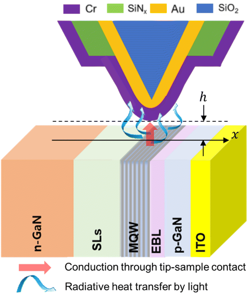 | ||
| Fig. 1 Heat transfer between the tip of the SThM probe scanning across the MQW and the cross section of an operating LED. Between the tip of the SThM probe and the cross section of an operating LED, radiative heat transfer occurs due to the intense light emitted locally from the MQW, as well as conduction heat transfer through the contact between the probe tip and the cross section of the LED. To verify the possibility of quantitative temperature mapping around MQW with two scans even in the presence of heat transfer via intense light locally emitted from the MQW, the effects of the distance h between the probe tip and the cross section of the LED and the lateral position x of the probe tip on the temperature measured by the SThM probe must be determined. | ||
Fig. 2 shows a schematic of the experimental setup for the VNP SThM under the conditions of a controlled vacuum, the circuit for AC heating and DC thermoelectric signal extraction from the thermocouple of the SThM probe, and the circuit for LED operation and injection current monitoring. The temperature sensor (thermocouple) of the SThM probe is heated with an AC bias of 100 kHz. At such a high frequency, despite AC heating, there is no temperature oscillation corresponding to the frequency of the AC bias in the SThM probe, owing to the large thermal time constant of the thermocouple sensor of the SThM probe (∼10 ms). As shown in Fig. 2, C1 blocks any unwanted DC voltage that may exist in the AC bias and interfere with the thermoelectric voltage generated by the thermocouple of the SThM probe. L1 and C2 act as a low-pass filter to block the AC bias when measuring the thermoelectric voltage generated by the thermocouple of the SThM probe. To monitor the injection current, the voltage across the reference resistance (100 Ω) was measured during the LED operation.
 | ||
| Fig. 2 Experimental setup for vacuum null-point scanning thermal microscopy (VNP SThM) under controlled vacuum. The thermocouple of the SThM probe is heated with a high-frequency (100 kHz) AC bias. C1 blocks blocks unwanted DC voltages that may be present on the AC bias. L1 and C2 act as a low-pass filter to block high-frequency AC bias when measuring the thermoelectric voltage generated by the thermocouple of the SThM probe. The thermoelectric voltage generated by the thermocouple is directly amplified by an in-amp in the vacuum chamber before passing through the feed-through to minimize interference by external noise. | ||
The circuit for LED operation and injection current monitoring was electrically floated from the ground of the circuit for AC heating and DC thermoelectric signal extraction from the thermocouple of the SThM probe. If the circuit for LED operation and injection current monitoring is not electrically floated from the ground of the SThM probe, the current can suddenly flow because of the local potential difference between the tip of the SThM probe and the LED cross section. When this occurs, the thermocouple of the SThM probe is destroyed.
The SThM probe used in this study is the NP SThM02 probe developed by Chae et al. The cantilever and tip of the probe are composed of a 1.5 μm-thick silicon oxide film. The length and width of the cantilever of the probe are 200 μm and 20 μm, respectively. The height of the tip is 12 μm.33 A thermocouple junction composed of chromium and gold thin films is located at the apex of the tip. The diameter of the thermocouple junction is approximately 100 nm, and the tip radius of the NP SThM02 is approximately 65 nm. The heat-resistance temperature of the thermocouple junction of the NP SThM02 probe was ∼250 °C.
In this study, an LED sample with the same structure as that used by Jung et al. was used for comparison with the results reported by Jung et al.27 The epilayers of the GaN-based vertical LED used in this experiment were composed of a 2.5 μm-thick n-GaN layer, 110 nm-thick super lattices (SLs), 80 nm-thick MQW, 45 nm-thick electron blocking layer (EBL), 60 nm-thick p-GaN layer, and 60 nm-thick indium tin oxide (ITO) layer deposited on a sapphire substrate. To measure the temperature distribution across the MQW of an LED using VNP SThM, the cross section of the LED must be scanned with an SThM probe. Therefore, as shown in Fig. 2, an LED was cleaved, attached to a ceramic package such that the cross section of the LED was exposed upward, and mounted on the AFM.
Fig. 3a shows Tc(x) and Tl(x) at 100 nm and Tl(x) at 300 nm measured across the MQW of an LED operating at a current density of 10.2 A cm−2 in vacuum (8.9 × 10⁻² Torr). Tc(x) changes between 73.5 °C and 75.5 °C depending on x. However, Tl(x) at 100 nm and Tl(x) at 300 nm both maintain a nearly constant value of ∼82.7 °C. If Tl(x) has a constant value regardless of x, Tnc(x) corresponding to Tl(x) at h = 0 also has a constant value regardless of x.
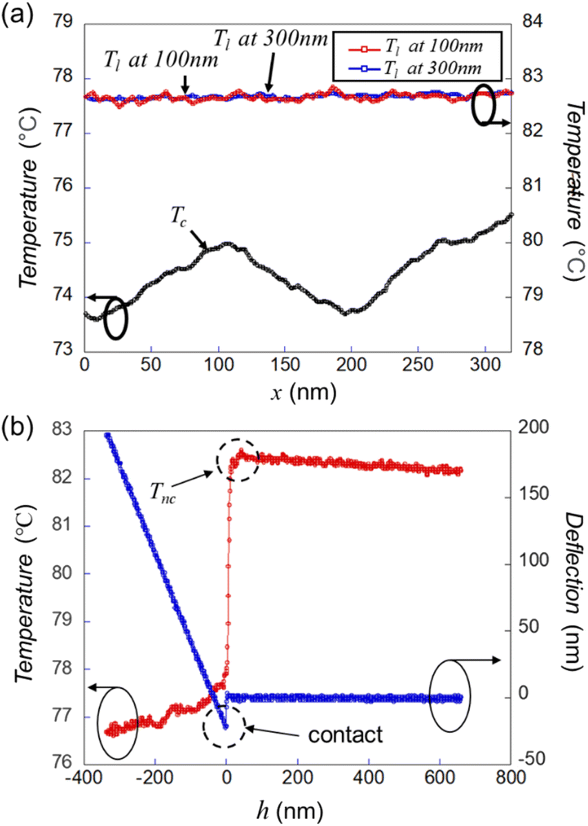 | ||
| Fig. 3 Dependence of Tl(x) and Tc(x) on x and h on the cross section of an LED in operation at the current density of 10.2 A cm−2 in vacuum (8.9 × 10⁻² Torr). (a) Dependence of Tl(x) and Tc(x) on x. Tc(x) shows a distinct dependence on x; Tl(x) shows little dependence on x except for measurement noise. (b) Dependence of Tl(x) and Tc(x) on h. A negative temperature jump Tj (≡ Tc − Tnc) occurs instantaneously when the tip of the SThM probe touches the cross section of the LED. This means that the temperature of the probe tip is higher than the temperature of the cross section of the LED. Until the tip of the SThM probe touches the cross section of the LED, Tl(x) increases slowly with decreasing h. | ||
Therefore, the measurement results shown in Fig. 3a indicate that only Tc1(x) and Tc2(x) depend on x in eqn (1), even across the MQW on the cross section of the LED that locally emits intense light. In addition, Tl(x) at 100 nm and Tl(x) at 300 nm almost overlap. This indicates that Tl(x) has a negligible dependence on h within this range. Hence, with two scans (Tc1(x) and Tc2(x)) using VNP SThM, the temperature distribution across the MQW of the LED in operation can be obtained.
If Tl(x) varied with x experimentally, this would also be a very interesting result. As explained by Jung et al., eqn (1) is valid even when there is heat transfer by radiation.27 In addition, as demonstrated experimentally by Cha et al., Tl(x) is independent of x when there is no heat transfer by local intense radiation in vacuum.28 Therefore, the change in Tl(x) with x in vacuum should be due to the spatial change in local radiation. This would have meant that the spatial variation in the light intensity emitted from the MQW could be measured by the SThM probe with nanoscale resolution. However, no change in Tl(x) with x due to the spatial change of local radiation was observed.
When the LED is turned off, Tl(x) does not depend on x or h, as in the case of Cha et al., and remains almost constant at ∼40 °C. A temperature rise of ∼20 °C above room temperature is attributable to the heating of the SThM probe by the red laser used for position control.
Fig. 3b shows the temperature measured by the SThM probe and the deflection of the SThM probe as a function of the distance h between the tip of the SThM probe and the cross section of the LED when the LED is operated with an injection current of 10.2 A cm−2 at a vacuum of 8.9 × 10⁻² Torr. By definition, Tl corresponds to Tnc immediately before the tip of the SThM probe touches the sample (h = 0), and Tl corresponds to Tc immediately after the tip touches the sample. The negative value of the temperature jump Tj (≡ Tc − Tnc) that occurs when the tip of the SThM probe touches the sample indicates that the temperature of the tip is higher than the temperature of the LED cross section. As shown in Fig. 5b and 6b, the actual temperature of the epilayers on the cross section of an LED in operation at an injection current of 10.2 A cm−2 measured using the VNP SThM varies between 35 and 40 °C depending on x. This means that the temperature on the cross section of the LED during operation is not high at this current density; however, the tip of the SThM probe is heated to a temperature higher than that of the cross section by the light emitted from the MQW.
According to the measurement results shown in Fig. 3b, Tl decreases slowly as the distance h between the tip of the SThM probe and the cross section of the LED increases. Cha et al. observed negligible dependence of Tl on h. However, in this case, the dependence of Tl on h was small but observable. This is because the heating of the probe tip by the light emitted from the MQW gradually decreases as h increases. The reason for the decrease in heating of the tip is presumed to be that the solid angle of the tip to the MQW decreases as h increases. Therefore, in this study, the same experiment as that shown in Fig. 3b was performed as required, and Tl at h = 0, indicated by the dotted line in Fig. 3b, was set to Tnc.
As demonstrated above, the measurement results in Fig. 3a confirmed that Tnc(x) had a constant value regardless of the lateral position x of the probe tip during scanning, even in the presence of intense light from the MQW. Therefore, as in the case of Cha et al., Ts(x) can be obtained using eqn (1) with only two scans even at a fairly low vacuum (∼10−1 Torr).28 However, unlike the case of Cha et al., as shown in Fig. 3b, it is confirmed that the dependence of Tnc(x) on h is weak but can exist.
Therefore, in this study, the 2 scans required to obtain Ts(x) in vacuum (8.9 × 10⁻² Torr) using eqn (1) is performed in the following order: Scan SThM probe in contact mode without intentionally heating the probe and obtain Tc1(x). Measure the temperature using the SThM probe as a function of the distance h between the tip of the SThM probe and the cross section of an LED in operation and obtain Tnc1(x), which is the temperature measured immediately before the tip of the SThM probe touches the sample (h = 0). Heat the SThM probe to a different degree. Scan SThM probe in contact mode and obtain Tc2(x). Measure the temperature using the SThM probe as a function of the distance h between the tip of the SThM probe and the cross section of an LED in operation and obtain Tnc2(x).
Result
We demonstrated that VNP SThM could be performed with two scans across the MQW on the cross section of the LED in operation and measured the change in the two-dimensional temperature distribution across the MQW as the injection current was increased systematically over four stages.As shown in Fig. 4, the external quantum efficiency (EQE) of the LED used in this study peaks at an injection current of 3.48 A cm−2 and then decreases as the injection current increases. We measured the temperature distribution around the MQW at four injection current densities: 3.48, 10.02, 15.38, and 22.09 A cm−2, where the EQE was measured.
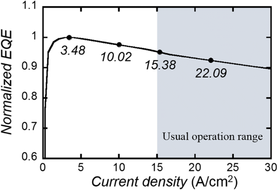 | ||
| Fig. 4 Measured external quantum efficiency (EQE) of the LED. The measured EQE is normalized by the EQE at a current density of 3.48 A cm−2, where the EQE reaches its peak. The grey area is the normal operation range. (Reproduced from ref. 27 with permission from American Institute of Physics). | ||
Two-dimensional graphs of Tc1, Tc2, and Ts obtained at four injection current densities are shown in Fig. 5. Ts is obtained by substituting Tc1 and Tc2 along with Tnc1 and Tnc2 measured immediately before or after performing the scans, for Tc1 and Tc2 in eqn (1).
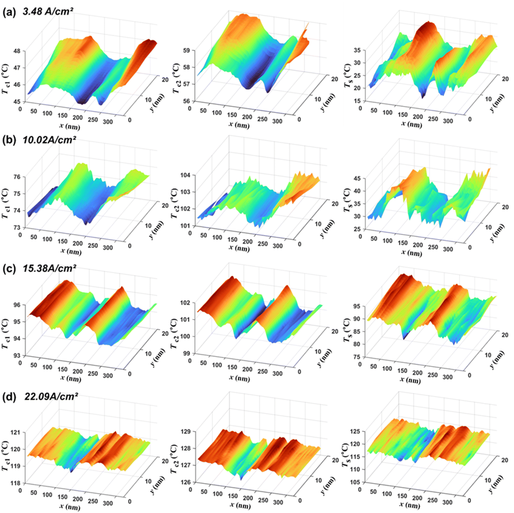 | ||
| Fig. 5 Two-dimensional graphs of Tc1, Tc2, and Ts obtained at four injection current densities. Ts is obtained by substituting Tc1 and Tc2 along with Tnc1 and Tnc2 measured separately into eqn (1). (a) At 3.48 A cm−2, Tnc1 = 49.7 °C and Tnc2 = 63.9 °C. (b) At 10.02 A cm−2, Tnc1 = 82.7 °C and Tnc2 = 115.8 °C. (c) At 15.38 A cm−2, Tnc1 = 96.1 °C and Tnc2 = 103.6 °C. (d) At 22.09 A cm−2, Tnc1 = 120.0 °C and Tnc2 = 129.3 °C. Tc1 and Tc2 appear qualitatively similar to Ts in their changes. However, Tc1 and Tc2 differ from Ts in the magnitude of change, rate of change, and absolute value. | ||
As shown in Fig. 5, Tc1 and Tc2 appear qualitatively similar to Ts in their changes. However, the magnitude of change, rate of change, and absolute values of Tc1 and Tc2 are significantly different from those of Ts, which is the actual surface temperature obtained from eqn (1). This is because Tc1 and Tc2 are affected by not only the local heat transfer through the contact between the tip of the probe and cross section of the LED but also the light emitted from the MQW, red laser required for position control, and electrical heating of the probe. In addition, even the temperature signal due to local heat transfer through the contact between the tip of the probe and LED cross section is influenced by not only the local temperature of the LED cross section but also the local contact thermal resistance and local spreading thermal resistance of the sample. However, as previously mentioned, eqn (1) enables the quantitative measurement of the unperturbed temperature of the sample, even when there is heat transfer through air or by light, and the contact thermal resistance between the tip of the probe and the sample and the spreading thermal resistance of the sample are unknown and change. Therefore, when analyzing the temperature distribution across the MQW of an LED during operation, Tc is not appropriate, and Ts must be used.
In principle, because the active layers of the LED used in this study have a one-dimensional structure, the temperature distribution across the MQW of the LED should also be a function of x. However, the measured temperature distributions shown in Fig. 5 are not completely one-dimensional. This is primarily because the roughness of the cross-sectional surface causes measurement noise. Previously, Cha et al. experimentally demonstrated that the VNP SThM could be used to measure the unperturbed quantitative temperature distribution regardless of the topography.28 However, the roughness of the sample surface still seems causing noise in the measurement owing to the irregularity of the tip–sample contact. In the process of exposing the LED cross section through cleaving, we attempted to obtain as flat a cross section as possible; however, the resulting LED cross section was not completely flat.
The temperature distributions in Fig. 5 show that the overall temperature across the MQW of the LED increased as the current density increased, and the location of the temperature peak shifted significantly. For a more facile analysis of the effect of the nanostructures constituting the epilayers on the change in the temperature distribution with increasing current density, the two-dimensional temperature distribution at each current density in Fig. 5 is superimposed with respect to the positions of the nanostructures constituting the epilayers. Furthermore, the temperature distribution is redrawn into a one-dimensional temperature distribution, as shown in Fig. 6.
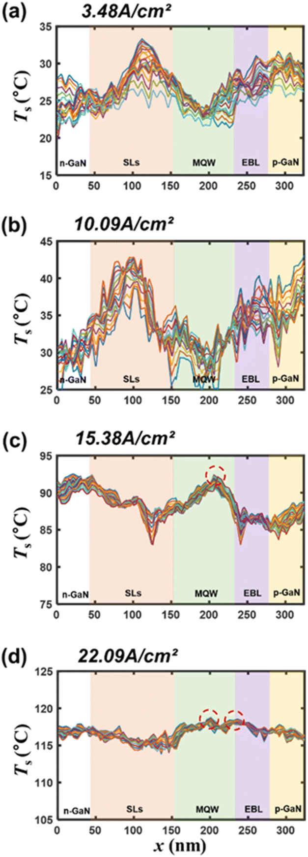 | ||
| Fig. 6 One-dimensional temperature distributions obtained by superimposing the two-dimensional temperature distributions across the multi-quantum well (MQW) of a light-emitting diode (LED) in operation with respect to the position of the nanostructures constituting the epi-layers at four different injection current densities: (a) 3.48, (b) 10.02, (c), 15.38, and (d) 22.09 A cm−2. In the cases of current densities at 3.48 and 10.02 A cm−2, the temperatures of the SL and p-GaN regions, which have high electrical resistance, appear high. At a current density of 15.38 A cm−2, the overall increase in temperature is significant, whereas the location of the temperature peak occurs in the MQW, as indicated by the red dashed circle. At a current density of 22.09 A cm−2, the temperature peaks not only in the MQW but also near the interface between the MQW and electron-blocking layer, as indicated by the red dashed circles. | ||
At a current density of 3.48 A cm−2, as shown in Fig. 6a, the temperature across the MQW of the LED is low overall, and the temperatures in the MQW and n-GaN regions are the lowest. This may be because the rate at which the current injected into the MQW is dissipated as heat is small because the EQE is maximum at this current density. By contrast, the temperatures of the SL and p-GaN regions are relatively high because the electrical resistance of these regions is relatively high.
At a current density of 10.02 A cm−2, as shown in Fig. 6b, the overall increase in temperature is ∼5 °C, in contrast to the case of a current density of 3.48 A cm−2, and the temperature distribution is similar to that at a current density of 3.48 A cm−2. At this current density, the rate at which the current injected into the MQW dissipates as heat remains still low.
At a current density of 15.38 A cm−2, as shown in Fig. 6c, the overall increase in temperature is considerable, ∼50 °C, in contrast to the case of a current density of 10.02 A cm−2. The significant overall temperature increase indicates that the rate at which the injected current dissipates as heat increases significantly. The temperature distribution was also considerably different from that at a current density of 3.48 A cm−2 or the one at 10.02 A cm−2. At the two relatively low current densities, the temperature was relatively high in the SL and p-GaN regions. However, in this case, the temperature peaked distinctly in the MQW. The significant change in the relative temperature distribution indicates that the main cause of the dissipation of electrical energy as heat has changed. As the current density increases, the proportion of electrical energy dissipated as heat increases to a greater extent in the MQW region than in the SL and p-GaN regions.
At a current density of 22.09 A cm−2, as shown in Fig. 6d, the overall increase in temperature is ∼25 °C, in contrast to the case of a current density of 15.38 A cm−2. The relative temperature distribution is somewhat different from that at a current density of 15.38 A cm−2. At a current density of 15.38 A cm−2, the temperature peaks only in the MQW region; however, in this case, the temperature peaks not only in the MQW region but also near the interface between the MQW region and EBL. This is probably due to the leakage current. As the current density increases, the rate of electrons flowing through the MQW into the EBL increases, resulting in an increased rate of phonon generation in the EBL, and consequently, a temperature peak near the EBL.
Conclusions
In this study, we rigorously demonstrated that VNP SThM could quantitatively map two-dimensional temperature distribution with high thermal sensitivity and nanoscale resolution, even in the presence of locally varying strong light emissions, such as the cross section of an operating LED. Subsequently, using VNP SThM, we mapped the temperature distribution around the MQW on the cross section of an LED in operation for each injection current while increasing the injection current of the LED in four steps. The measurement results of the temperature distribution around the MQW clearly show that as the injection current increased, the overall temperature around the MQW increased significantly, and the temperature peak position shifted. These results directly show that the main cause of the dissipation of electrical energy into thermal energy inside the LED changes as the injection current increases, and the nanostructures inside the LED affect the dissipation of electrical energy into thermal energy. We anticipate that the high thermal sensitivity, nanoscale resolution, and convenience of VNP SThM will enable the direct observation of the effect of nanostructures inside various types of nanophotonic devices on local energy conversion even under intense localized radiation.Author contributions
Hwijong Shin: investigation, methodology, data curation, formal analysis, visualization, writing – original draft. Seosi Liu: methodology, data curation, visualization, formal analysis. writing – original draft. Ohmyoung Kwon: investigation, conceptualization, methodology, writing – original draft, writing – review & editing, supervision, resources, funding acquisition.Conflicts of interest
There are no conflicts to declare.Acknowledgements
This research was supported by the Basic Science Research Program (NRF-2021R1H1A2093422) through the National Research Foundation of Korea (NRF), funded by the Ministry of Education, Science and Technology.References
- D. A. Steigerwald, J. C. Bhat, D. Collins, R. M. Fletcher, M. O. Holcomb, M. J. Ludowise, P. S. Martin and S. L. Rudaz, IEEE J. Sel. Top. Quantum Electron., 2002, 8, 310–320 CrossRef CAS.
- M. H. Crawford, IEEE J. Sel. Top. Quantum Electron., 2009, 15, 1028–1040 CAS.
- S. Pimputkar, J. S. Speck, S. P. Denbaars and S. Nakamura, Nat. Photonics, 2009, 3, 180–182 CrossRef CAS.
- M. Kneissl, T. Y. Seong, J. Han and H. Amano, Nat. Photonics, 2019, 13, 233–244 CrossRef CAS.
- T. Wu, C. W. Sher, Y. Lin, C. F. Lee, S. Liang, Y. Lu, S. W. H. Chen, W. Guo, H. C. Kuo and Z. Chen, Appl. Sci., 2018, 8, 1557 CrossRef.
- Y. Huang, E. L. Hsiang, M. Y. Deng and S. T. Wu, Light Sci. Appl., 2020, 9, 105 CrossRef CAS PubMed.
- J. Piprek, Phys. Status Solidi A, 2010, 207, 2217–2225 CrossRef CAS.
- J. Cho, E. F. Schubert and J. K. Kim, Laser Photonics Rev., 2013, 7, 408–421 CrossRef CAS.
- G. Verzellesi, D. Saguatti, M. Meneghini, F. Bertazzi, M. Goano, G. Meneghesso and E. Zanoni, J. Appl. Phys., 2013, 114, 071101 CrossRef.
- Y. C. Shen, G. O. Mueller, S. Watanabe, N. F. Gardner, A. Munkholm and M. R. Krames, Appl. Phys. Lett., 2007, 91, 141101 CrossRef.
- M. Binder, A. Nirschl, R. Zeisel, T. Hager, H. J. Lugauer, M. Sabathil, D. Bougeard, J. Wagner and B. Galler, Appl. Phys. Lett., 2013, 103, 071108 CrossRef.
- J. Iveland, L. Martinelli, J. Peretti, J. S. Speck and C. Weisbuch, Phys. Rev. Lett., 2013, 110, 177406 CrossRef PubMed.
- J. Iveland, M. Piccardo, L. Martinelli, J. Peretti, J. W. Choi, N. Young, S. Nakamura, J. S. Speck and C. Weisbuch, Appl. Phys. Lett., 2014, 105, 052103 CrossRef.
- G. B. Lin, D. Meyaard, J. Cho, E. Fred Schubert, H. Shim and C. Sone, Appl. Phys. Lett., 2012, 100, 161106 CrossRef.
- D. S. Meyaard, G. B. Lin, J. Cho, E. Fred Schubert, H. Shim, S. H. Han, M. H. Kim, C. Sone and Y. Sun Kim, Appl. Phys. Lett., 2013, 102, 251114 CrossRef.
- Y. Huang, Z. Liu, X. Yi, Y. Guo, S. Wu, G. Yuan, J. Wang, G. Wang and J. Li, Mod. Phys. Lett. B, 2016, 30, 1650221 CrossRef CAS.
- J. Yun, J. I. Shim and H. Hirayama, Appl. Phys. Express, 2015, 8, 022104 CrossRef CAS.
- A. Pandey, A. Aiello, J. Gim, R. Hovden, E. Kioupakis, P. Bhattacharya and Z. Mi, 2020 IEEE Photonics Conf. IPC 2020 – Proc., 2020, 12, pp. 1–7 Search PubMed.
- L. Wang, J. Jin, C. Mi, Z. Hao, Y. Luo, C. Sun, Y. Han, B. Xiong, J. Wang and H. Li, Materials, 2017, 10, 1233 CrossRef PubMed.
- T. E. Nee, J. C. Wang, B. Y. Zhong, J. J. Hsiao and Y. F. Wu, Nanomaterials, 2021, 11, 1449 CrossRef CAS PubMed.
- J. Piprek, Materials, 2020, 13, 1–18 CrossRef PubMed.
- B. Galler, P. Drechsel, R. Monnard, P. Rode, P. Stauss, S. Froehlich, W. Bergbauer, M. Binder, M. Sabathil, B. Hahn and J. Wagner, Appl. Phys. Lett., 2012, 101, 131111 CrossRef.
- Z. Liu, T. Wei, E. Guo, X. Yi, L. Wang, J. Wang, G. Wang, Y. Shi, I. Ferguson and J. Li, Appl. Phys. Lett., 2011, 99, 091104 CrossRef.
- J. Bodzenta and A. Kazmierczak-Bałata, J. Appl. Phys., 2022, 132, 140902 CrossRef CAS.
- L. Shi and A. Majumdar, J. Heat Transf., 2002, 124, 329–337 CrossRef CAS.
- J. Chung, K. Kim, G. Hwang, O. Kwon, Y. K. Choi and J. S. Lee, Int. J. Therm. Sci., 2012, 62, 109–113 CrossRef.
- E. Jung, G. Hwang, J. Chung, O. Kwon, J. Han, Y.-T. Moon and T.-Y. Seong, Appl. Phys. Lett., 2015, 106, 41114 CrossRef.
- J. Cha, H. Shin and O. Kwon, Int. J. Therm. Sci., 2022, 172, 107268 CrossRef.
- G. Hwang and O. Kwon, Int. J. Therm. Sci., 2016, 108, 81–88 CrossRef CAS.
- K. Yoon, G. Hwang, J. Chung, H. G. Kim, O. Kwon, K. D. Kihm and J. S. Lee, Carbon, 2014, 76, 77–83 CrossRef CAS.
- G. Hwang and O. Kwon, Nanoscale, 2016, 8, 5280–5290 RSC.
- K. Kim, J. Chung, G. Hwang, O. Kwon and J. S. Lee, ACS Nano, 2011, 5, 8700–8709 CrossRef CAS PubMed.
- H. Chae, G. Hwang and O. Kwon, Ultramicroscopy, 2016, 171, 195–203 CrossRef CAS PubMed.
Footnote |
| † These authors have contributed equally to this work. |
| This journal is © The Royal Society of Chemistry 2023 |