
 Open Access Article
 This Open Access Article is licensed under a Creative Commons Attribution-Non Commercial 3.0 Unported Licence
Advances in solar energy harvesting integrated by van der Waals graphene heterojunctions
Top Khac Le†
 ab,
The-Hung Mai†c,
Muhammad Aamir Iqbald,
Dimitra Vernardoue,
Van-Duong Daof,
Vinoth Kumar Ponnusamy*ghi,
Chandra Sekhar Rout*j and
Phuong V. Pham*c
ab,
The-Hung Mai†c,
Muhammad Aamir Iqbald,
Dimitra Vernardoue,
Van-Duong Daof,
Vinoth Kumar Ponnusamy*ghi,
Chandra Sekhar Rout*j and
Phuong V. Pham*c
aFaculty of Materials Science and Technology, University of Science, Ho Chi Minh City 700000, Vietnam
bVietnam National University, Ho Chi Minh City 700000, Vietnam
cDepartment of Physics, National Sun Yat-sen University, Kaohsiung 80424, Taiwan. E-mail: phuongpham@mail.nsysu.edu.tw
dSchool of Materials Science and Engineering, Zhejiang University, Hangzhou 310027, China
eDepartment of Electrical and Computer Engineering, School of Engineering, Hellenic Mediterranean University, Heraklion 71410, Greece
fFaculty of Biotechnology, Chemistry, and Environmental Engineering, Phenikaa University, Hanoi 100000, Vietnam
gDepartment of Medicinal and Applied Chemistry and Research Center for Precision Environmental Medicine, Kaohsiung Medical University, Kaohsiung 807, Taiwan. E-mail: kumar@kmu.edu.tw
hDepartment of Medical Research, Kaohsiung Medical University Hospital, Kaohsiung 807, Taiwan
iDepartment of Chemistry, National Sun Yat-sen University, Kaohsiung 80424, Taiwan
jCentre for Nano and Material Sciences, Jain University, Bangalore 562112, India. E-mail: r.chandrasekhar@jainuniversity.ac.in
First published on 27th October 2023
Abstract
Graphene has garnered increasing attention for solar energy harvesting owing to its unique features. However, limitations hinder its widespread adoption in solar energy harvesting, comprising the band gapless in the molecular orbital of graphene lattice, its vulnerability to oxidation in oxidative environments, and specific toxic properties that require careful consideration during development. Beyond current challenges, researchers have explored doping graphene with ionic liquids to raise the lifespan of solar cells (SCs). Additionally, they have paid attention to optimizing graphene/Si Schottky junction or Schottky barrier SCs by enhancing the conductivity and work function of graphene, improving silicon's reflectivity, and addressing passivation issues at the surface/interface of graphene/Si, resulting in significant advancements in their power conversion efficiency. Increasing the functional area of graphene-based SCs and designing efficient grid electrodes are also crucial for enhancing carrier collection efficiency. Flaws and contaminants present at the interface between graphene and silicon pose significant challenges. Despite the progress of graphene/Si-based photovoltaic cells still needs to catch up to the efficiency achieved by commercially available Si p–n junction SCs. The low Schottky barrier height, design-related challenges associated with transfer techniques, and high lateral resistivity of graphene contribute to this performance gap. To maximize the effectiveness and robustness of graphene/Si-based photovoltaic cells, appropriate interlayers have been utilized to tune the interface and modulate graphene's functionality. This mini-review will address ongoing research and development endeavors using van der Waals graphene heterojunctions, aiming to overcome the existing limitations and unlock graphene's full potential in solar energy harvesting and smart storage systems.
1. Introduction
Climate change mitigation, increasing demand for energy, and global energy transformation are driving forces toward an array of alternative renewable energy sources other than traditional fossil fuels. Despite numerous availability sustainable energy resources, solar energy is recognized as a representative environmentally-friendly energy source with inexhaustible and fewer limitations compared to other alternatives such as wind and hydro. This has caught the attention of both scientific and industrial community's bio-friendly and renewable nature to the identification of solar energy harvesting devices as the holistic and cleanest energy sources to explore in serious global energy crisis terms (Fig. 1). In this context, the quest for innovative and sustainable energy in taking advantage of existing traditional carbon systems has been the center for advancing solar cells (SCs) and photovoltaic (PV) technologies to address the ever-increasing need for environmentally friendly and emission-free energy.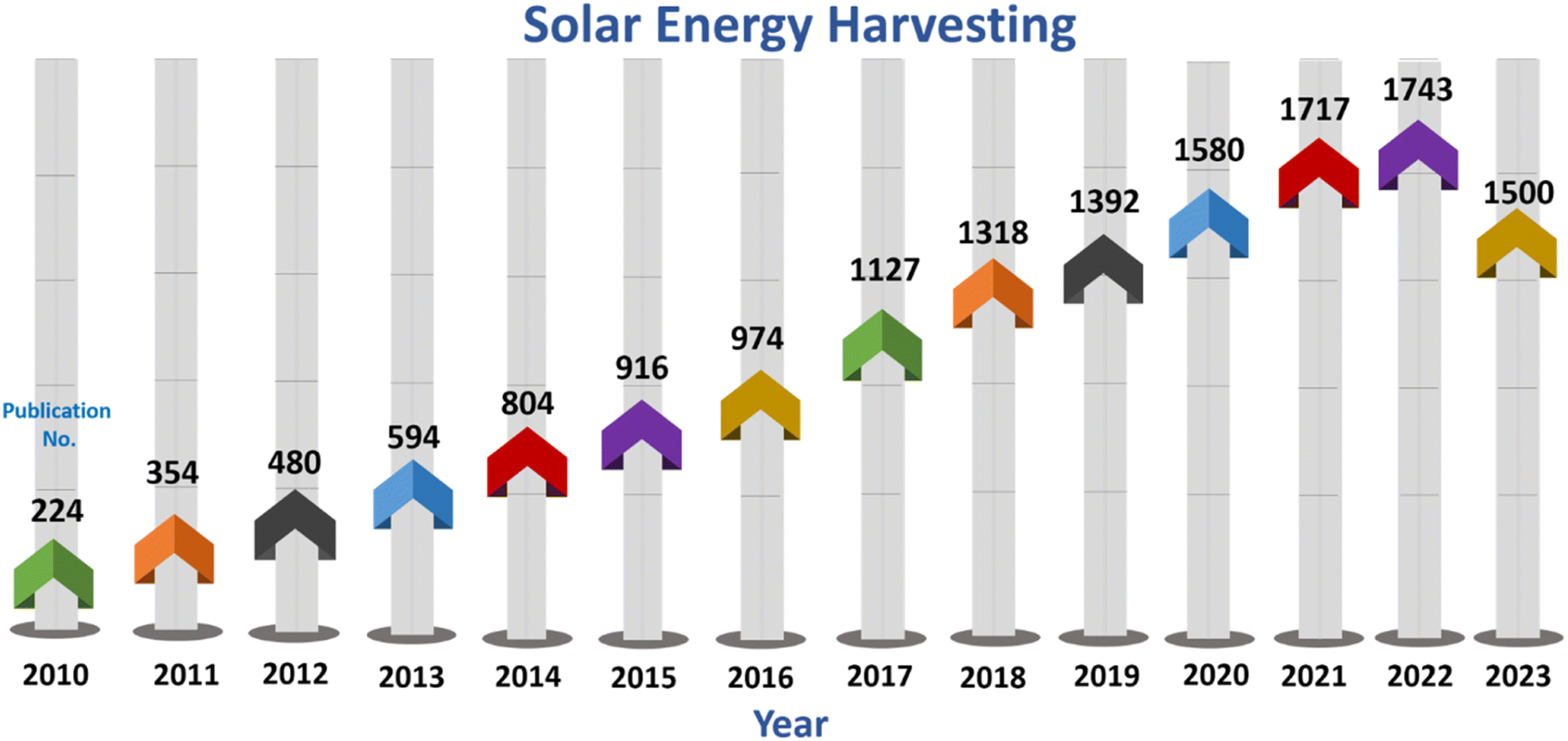 | ||
| Fig. 1 The publication numbers of “solar energy harvesting” in terms of 2010–2023 (WOS Source). | ||
However, the classification of SCs is organized into three categories of generations.1 The first category comprises single- and poly-crystalline Si, which boast the highest efficiency level (26.6%).2 The next classification refers to SCs that employ a cadmium telluride thin film (CdTe) and copper indium gallium selenide (CIGS) with the highest reported performance (23.35%).3 Including various sub-categories, the third category involves the SCs based on newly found materials and has been widely explored to enhance the efficiency of SCs.4 In addition, SCs using 2D materials e.g., MoS2, WSe2, and graphene are classified in a diverse category.5–9 Currently, research and development (R&D) as along with commercialization activities of Si-based SCs are mostly directed in enhancing the power conversion efficiency (PCE) while reducing manufacturing expenses.10 Interestingly, graphene has been found to be a promising candidate to revolutionize the SC market. Extensive studies have examined the integration of graphene into Si PV technology, motivated by the extraordinary physical properties of graphene. These attributes encompass exceptional electrical conductivity, carrier mobility, thermal conductivity, mechanical flexibility, stability, and dominant transmittance (97.7% monolayer graphene in visible region).11–13 Thus, the R&D efforts focused on incorporating graphene into devices used for SCs have rapidly progressed, resulting in high PCEs exceeding 15% in copious distinguished applications. Several works associated with incorporating of graphene into PVs for numerous vital roles, such as the active layer and electrode, have been reported.14–16
One crucial challenge in creating high-performance SCs for energy harvesting and practical implementations is the efficient generation/separation of paired electron–hole from photo-induced processes, followed by the effective transfer of these separated charge carriers to the electrodes. In this context, graphene revealed significant improvement. Consequently, research has been performed to explore and evaluate the graphene/Si Schottky junction (G/S-SJ) device for various applications utilizing the internal photoemission process. Hence, SCs that utilize a SJ, with graphene acting as a metal and Si as a semiconductor, have been duly recognized as a suitable example of Schottky junction devices (SJDs).17
In this review, the emergence of G/S SB-SCs and PVs concerns are exhibited in relation to the extensive endeavors to enhance the performance of low-cost SCs. The charge transport mechanism in G/S SB-SCs is elucidated, along with several approaches that facilitate the optimization of such devices for PCE to explore the further mechanism principle of the heterostructured devices. Additionally, the difficulties and potential opportunities associated with G/Si SB-SCs in the field of PV technology are discussed, with the aim of paving the way for the design of next-generation solar energy harvesting systems.
2. Emergence of graphene/Si in solar cells and photovoltaics
Among the different 2D materials, graphene, a well-known carbon allotropes, was first fabricated in 2004 by Novoselov et al. using mechanical exfoliation of graphite.11 It comprises a monolayer of carbon atoms arranged in a hexagon network.7,18–42 Thus, graphene has been shown as a greatly promising material for future optoelectronic devices due to its remarkable features, including high mobility reaching up to 104 cm2 V−1 s−1 at ambient temperature, exceptional thermal and electric conductivities, and ballistic transport.12,43 Also, in the broad spectra range of visible and near-infrared (NIR), the transmittance of single layer graphene can reach 97.7%, and only 2.3% of the light intensity can be absorbed.44,45 As a result of its thin structure, graphene enables a substantial section of sunlight to permeate through it.46 The exceptional optical and electronic features of graphene have positioned it as a highly favorable prospect for the design and production of SCs. Graphene has a dual role, functioning as both a target electrode in Schottky junction or Schottky barrier solar cells (SB-SCs) and an active layer. Additionally, it possesses flexibility and is widely abundant on a global scale. This has inspired significant interest in substituting FTO and ITO substrates47 for producing high-performance and low-cost solar panels, including graphene/Si solar cells (G/S-SCs).48 Additionally, the capacity to adjust the ϕwf of graphene enables it to function as either p- or n-type electrodes.49 Additionally, graphene typically exhibits excellent environment stability,50 exceptional mechanical strength,51 and high crystalline quality during upscale compared with other 2D materials e.g., MoS2, WS2, WSe2, etc.52 These characteristics render graphene-based SCs advantageous over the first generation of PVs. As a result, there has been a substantial increase in the abundance of work conducted on G/S SCs recently.53–57Owing to its physical/chemical/mechanical features, graphene-based heterojunction SCs exhibited an good efficiency (18.5%) when combined with GaAs structure.58 After achieving positive results in research and development trials, a feasible manufacturing process for small-scale commercial production of thin-film and dye-sensitized photo-supercapacitors using graphene has been effectively developed and implemented.59–61 However, large-scale manufacturing of these SC types remains challenging to date. SB-SCs, which are made using the method of direct deposition of a transparency electrode or thin film of metal on a moderately doped semiconductor wafer, have gained significant attention in PVs.62 They have advantages over traditional p–n junction SCs in terms of being inexpensive and simple to manufacture.63 Nevertheless, conventional SB-SCs require a thick metal layer that hinders solar radiation absorption. Thus, ITO has been explored as an alternative, but its limited resources and fragile nature limit its application in flexible devices. To overcome these challenges, graphene sheets have been successfully employed in SB-SCs, permitting the production of cost-effective, flexible solar panels with excellent environmental stability, eco-friendliness, and efficiency exceeding 10%. The demand for flexible SCs in various applications including wearable/implantable microsystems and wireless sensor networks for IoT, makes G/Si SB-SCs highly attractive for the PVs market.
Recently, the vehement efforts have been proceeded to develop new-generation G/Si SB-SCs, with a signify attention on chemical doping techniques to achieve high Schottky barrier height and efficiency. However, the chemical-doped G/Si SCs often exhibit rapid degradation due to the oxidative nature of the dopants. An alternative promising strategy is being explored to develop the chemical-doping-free G/Si SCs, which exhibit stability over several months. Regrettably, the effectiveness of these SCs is limited due to the high electrical resistance of graphene films and the low Schottky barrier of the G/Si heterojunction. Recently researches show that the PCE of G/Si SCs has been enhanced by doping technique with PbS quantum dots64 and electrical-field doping with a liquid gate circuit.65 Chemical doping into the graphene can generate more acceptor carriers and improve conductivity. However, they have limitations including significant light loss and the instability of the integrated liquid medium that prevent them from being used in practice.66
On the other hand, doping effects caused by solid interactions have been documented in graphene-assisted heterojunctions e.g., MoF6/graphene67,68 and MoO3/graphene.69 This advancement's lack of chemical reactions offers a promising approach for achieving steady graphene doping. From this perspective, a study was conducted to explore the interactions in graphene/fluorographene heterostructures, targeting to improve the output of G/Si SCs. Interestingly, fluorographene is a novel derivative of graphene that features dipoles created by C–F bonds in graphite, making it one of the thinnest known insulators. It is made by revealing graphene to fluoride gases, and its electrical features are adjusted via its C/F ratio.68 Simulated studies have demonstrated the interactions between graphene with other 2D materials (graphene and MoS2). Notably, the F atoms present in fluorographene function as receptors of electrons, leading to the transfer of charge-coupled 2D elements onto fluorographene and potentially causing p-type doping. Density functional theory (DFT) was employed to examine the optical characteristics of graphene hexagonal boron nitride (h-BN) and fluorographene.70 Fluorographene exhibits exceptional capability in decoupling graphene from the substrate. These distinctive properties make fluorographene an attractive option for optimizing G/Si SCs.
The pioneering study by Zhu et al. in 2010 explored the feasibility of G/n-Si SB-SCs achieving an efficiency of 1.65%.48 G/Si SB-SCs hold promise for effectively separating charge carriers due to their substantial built-in potential. Graphene holds a key role for the efficiency of these SCs because it acts as both active layer and transparent electrode.71,72 This requires the graphene to exhibit more physical properties such as good photo-generated charge carriers, high electron mobiles safely electron transport. In less than 10 years, G/Si SB-SCs achieved up to 15% efficiency due to the 100 times greater than (approximately 2.5 × 105 cm2 V−1 s−1) of electron mobility comparing Si substrate.73 Graphene, being a zero-band-gap semiconductor, exhibits the remarkable ability to absorb light across a broad spectrum. Moreover, electrons within graphene can traverse several micrometers without scattering, showcasing its exceptional transport characteristics.74 SCs using graphene such as hole transporter based on G/Si structure were first created by depositing a graphene thin film on Si surface.48 However, the graphene layer exhibited higher sheet resistance (a few kΩ), negatively affecting its conductivity. Consequently, it impeded the flow of photo-generated current in G/Si SCs, leading to an extraordinary reduction in their PCE. Initially, researchers explored the chemical doping on a top graphene surface, which involved the introduction of a p-type dopant into the graphene material. However, HNO3 and bis-(trifluoromethane sulfonyl)amide (TFSA) are the most widely utilized dopants in G/Si SCs.75,76 By introducing a TFSA layer, the highest reported increase in efficiency (1.9% to 8.6%) of G/Si SCs with the use of doping was achieved. Also, several other dopants, such as boron doping77 and doping with chemicals such as SOCl2, HNO3, HCl, and H2O2 were introduced by various research groups.75,78 Coating the top surface of graphene with a dopant proved highly effective in reducing its resistance. However, despite the benefits of chemical doping, a significant limitation is its unsteadiness in the atmospheric media, leading to surface deterioration and eventually restoring the cell's efficiency to its initial value. For this reason, graphene oxide (GO) and Pt nanoparticles (NPs) have been recognized as suitable dopants for the top surface of G/Si SCs.79,80 In G/Si SCs, a transparent MoO3/Ag/MoO3 heterojunction layer over graphene was applied, resulting in an increased ϕwf, reduced series resistance, and improved efficiency (0.86 to 3.5%) of graphene.69 Bhopal et al.81 reported an increase in efficiency from 4.3 to 5.01% in G/Si SCs using an Ag/Ni electrode to decrease the contact resistivity. NiO-induced doping in G/Si SCs was employed to lower the series resistance, enhance the SJ quality as well as improve cell robustness.82 In particular, effect contact of metallization front electrodes provides a direct electrical contact between graphene layer and the Si substrate. This low-resistance contact improves charge carrier extraction and reduces series resistance, leading to enhanced solar cells performance. Moreover, the process of depositing a metal layer onto the front surface of solar cells is well-established and relatively straightforward. Common deposition techniques like sputtering or evaporation are widely used for this purpose. While the efficiency of solar cells through the using the chemical induced doping could also be improved by enhanced carrier mobility and tunable properties. NiO is a prime example for the doping method, which can significantly promote the mobility of charge carriers. Besides, NiO doping can mitigate carrier recombination at the graphene/Si interface. By reducing recombination, the efficiency of charge carrier extraction and collection increases, leading to higher overall solar cells performance. Nevertheless, the limitations of these two methods still exist, and affects to quality of energy conversion. Typically, the controllable thickness and shape of electrodes is extremely important, due to the depending on the thickness and layout of the metal front electrode, there is a possibility of shading some of the active solar cell area, which can decrease efficiency, or in the doping method, achieving uniform doping across the entire solar cells area can be challenging, and any non-uniformity might lead to performance variations. Additionally, the stability of the NiO-doped layer and its interaction with other materials need to be accessed for potential degradation over time, which could impact long-term performance of the solar cells. Therefore, choosing the appropriate method will depend on factors such as the specific cell design, the level of performance enhanced desired, fabrication complexity, material compatibility. Furthermore, ongoing research may lead to improvements and refinements in these methods over time.
3. Structure and mechanism in graphene/Si SB-SCs
Fig. 2a illustrates the structure of G/Si SCs.73 The fabrication of such a device primarily relies on the method outlined by Li et al.48 The process includes the application of wet transfer to move chemical vapor deposited (CVD) graphene onto he exposed SiO2/n-Si. This is followed by the addition of front/rear electrode deposition, establishing the graphene/n-Si heterojunction as illustrated in Fig. 2b.83 SiO2 layer was deposited on Si, and it was etched away using a buffered oxide etchant, exposing a suitable-sized Si window. Afterward, graphene is transferred to Si substrate, accompanied by undesired graphene etching. Normally, top-notch CVD produced graphene is employed and shifted using polymethylmethacrylate (PMMA) technique. To be more precise, the graphene grown on a metal foil (Cu) is first coated with PMMA through a spin-coated process. The copper foil is then dispersed in a copper etchant solution (CuSO4![[thin space (1/6-em)]](https://www.rsc.org/images/entities/char_2009.gif) :HCl:H2O) for a few hours and subsequently rinsed with deionized water. Then, the PMMA-casted graphene film is relocated on Si window and metal pad. Finally, the PMMA is extracted using acetone, and the G/Si SCs are cleaned with isopropyl alcohol (IPA) to complete the fabrication process. Fig. 2c provides a schematic representation of G/Si SB-SCs based on heterojunction structure using various interfacial layers, doping, and anti-reflection coatings.84 When graphene is in proximity to Si, carrier transfer occurs to align the Fermi levels (EF). Electrons originating from n-type Si migrate to graphene, generating an area with reduced electron concentration. As a result, an inherent electric field forms between graphene and Si. When subjected to light, the Si substrate absorbs photons, giving rise to the generation of new electron–hole pairs. Inside the region of electron depletion, the electrons and holes generated by light are swiftly separated due to the existing electric field and are directed towards the electrodes. This process leads to the creation of a photocurrent.
:HCl:H2O) for a few hours and subsequently rinsed with deionized water. Then, the PMMA-casted graphene film is relocated on Si window and metal pad. Finally, the PMMA is extracted using acetone, and the G/Si SCs are cleaned with isopropyl alcohol (IPA) to complete the fabrication process. Fig. 2c provides a schematic representation of G/Si SB-SCs based on heterojunction structure using various interfacial layers, doping, and anti-reflection coatings.84 When graphene is in proximity to Si, carrier transfer occurs to align the Fermi levels (EF). Electrons originating from n-type Si migrate to graphene, generating an area with reduced electron concentration. As a result, an inherent electric field forms between graphene and Si. When subjected to light, the Si substrate absorbs photons, giving rise to the generation of new electron–hole pairs. Inside the region of electron depletion, the electrons and holes generated by light are swiftly separated due to the existing electric field and are directed towards the electrodes. This process leads to the creation of a photocurrent.
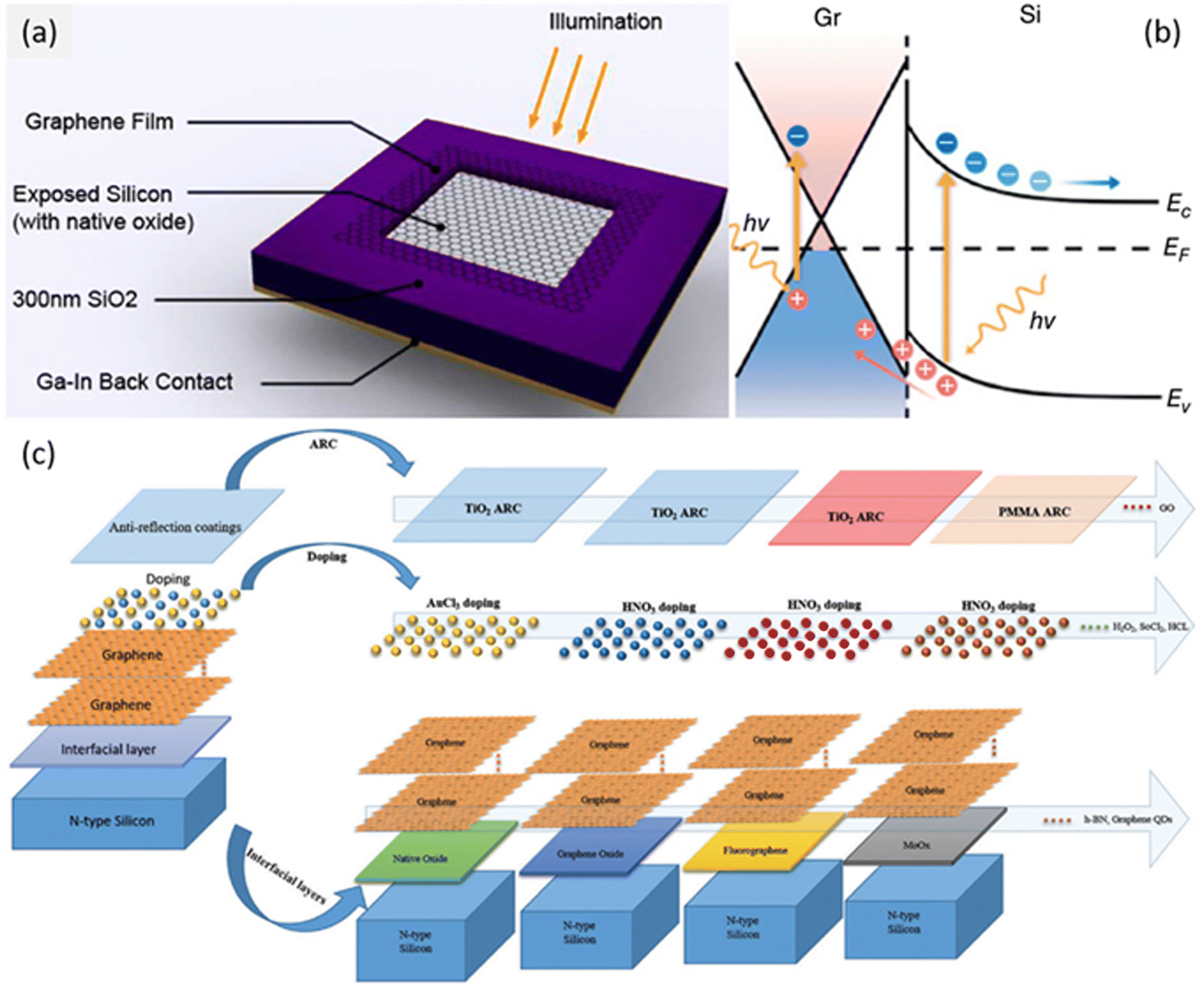 | ||
| Fig. 2 (a) Design of G/n-Si SC, a layer of graphene was applied onto SiO2/Si substrate, forming a junction. (a) has been reproduced from ref. 73 with permission from American Chemical Society. (b) Energy band diagram in G/n-Si SB-SCs and the displacement of electron–hole pairs. (b) has been reproduced from ref. 83 with permission from Wiley-VCH. (c) A visual representation depicting the uncomplicated creation of a G/Si SB-SCs through a heterojunction structure is shown. This process involves three key factors: interfacial layer, chemical doping, and ARC coating. These factors collectively contribute to improving efficiency and prolonging the durability of G/Si SCs. (c) reproduced from ref. 84 with permission from Royal Society of Chemistry. | ||
4. Performance parameters
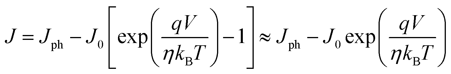
Dark current–voltage (I–V or J–V) of G/Si SJ was described by eqn (1).
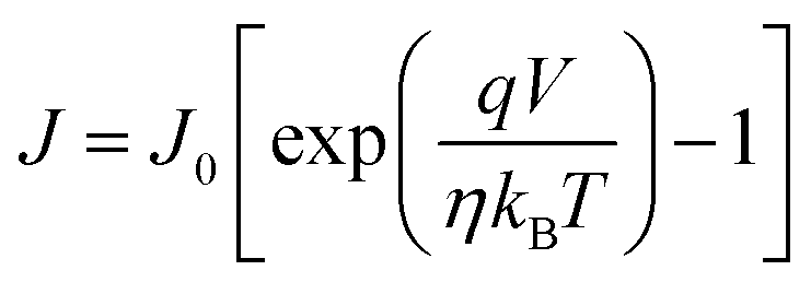 | (1) |
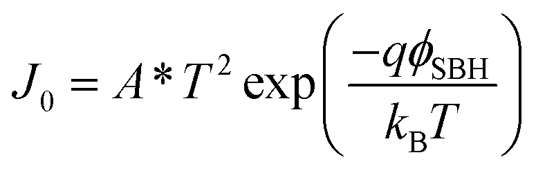 | (2) |
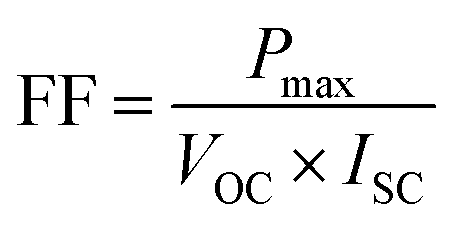
Electron/holes at regions of G/Si junction as light illuminated will generate the photovoltage (V) and it reaches maximum value in open-circuit voltage (VOC). As SC short-circuited, photogenerated carriers flow through the external circuit, resulting in a maximum current called ISC. Nevertheless, in practical use, SCs function within a range that lies between a short-circuit condition and an open-circuit condition. Due to the rectifying characteristics and non-linear voltage–current behavior of the G/Si junction, a maximum output power (Pmax) can be achieved.
PCE of the G/Si SCs quantifies the extent to which sunlight energy is changed into electricity. It can be conveyed using eqn (3).
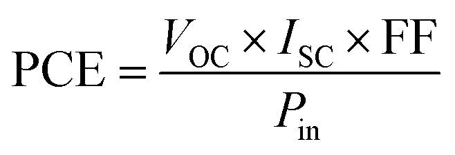 | (3) |
 | (4) |
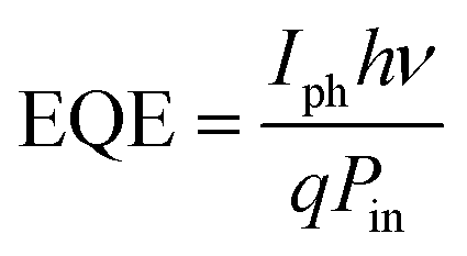
External quantum efficiency (EQE) is characterized as the ratio of charge carriers to incident photons of a specific energy, and its determination can be achieved through the utilization of eqn (5).
 | (5) |
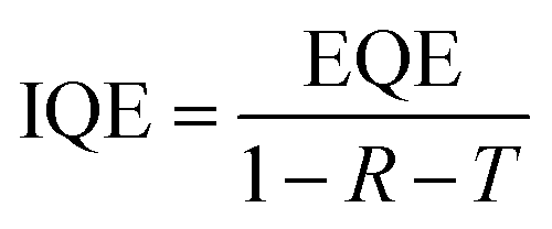
Internal quantum efficiency (IQE) refers to the count of charge carriers for each absorbed photon within the SC. IQE is evaluated by subtracting the photons lost due to reflection and transmission from the EQE. This connection can be mathematically represented using eqn (6).
 | (6) |
5. Theoretical efficiency limits of graphene/Si SCs
According to Shockley–Queisser (SQ) model, the PCE of SCs depends on the band gap of the active semiconductor layer. Auger recombination is also considered in reassessing the efficiency limits, resulting in the highest theoretical values for VOC, JSC, FF, and PCE. Other parameters such series resistance (RS) and shunt resistance (RSH) strongly affects the final current of SCs as contact with other devices. The current–voltage characteristics of SCs are described by eqn (7) and (8), representing the scenarios excluding extraneous resistances and considering both RS and RSH, respectively. In this context, Rs and RSH will be treated as a constant in the simplicity of SQ model for simplicity of mathematical treatment.
 | (7) |
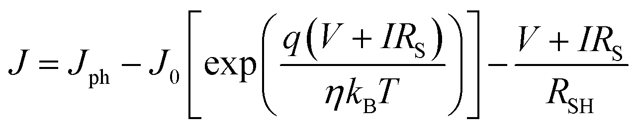 | (8) |
Fig. 3a and b displays the J–V curves of G/Si SCs for varying RS and RSH values, respectively.83 It is evident that the FF of the SCs exhibits a significant relationship with sheet resistance of graphene. Reducing the sheet resistance leads to increased FF, indicating that improving graphene's sheet resistance can be accomplished by focusing on high-quality growth, precise transfer, and controlled doping technique. The impact of shunt resistance transforms into relevance only when the resistance decreases below 10 kΩ. Otherwise, it has minimal to minimal results on the efficiency of G/Si SCs regardless of any variation in resistance. Given the provided experimental values for parasitic resistance (Rs = 10.5 Ω, Rsh = 45 MΩ), it can be concluded that the impact of series resistance on efficiency is significantly more detrimental (Fig. 3c).
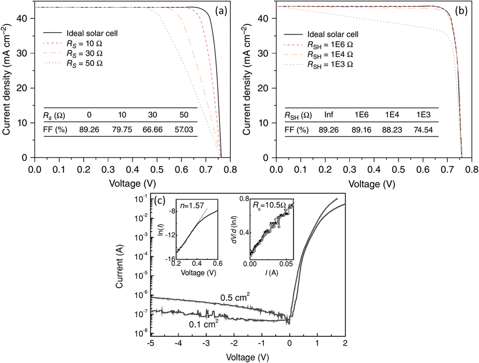 | ||
| Fig. 3 Voltage–current characteristics and FF of a theoretical G/Si SCs with various (a) series resistance, (b) sheet resistance. (a) and (b) have been reproduced from ref. 83 with permission from Wiley-VCH. Experimental G/Si SCs with (c) series resistance and sheet resistance, which is estimated from the reverse bias I–V sweep. (c) has been reproduced from ref. 48 with permission from Wiley-VCH. | ||
6. Strategies for enhancing efficiency of graphene/Si SCs
The SC efficiency was affected by absorption, hole–electro pair generation, diffusion of electron, lifetime of electron, etc. Recently research show strategies to enhance the performance of G/Si SCs such as doping in graphene material, and light trapping in Si substrate.6.1. Influence of dopants
Graphene serves as both transparent conductor and junction layer in G/Si SCs. As a transparent conductor, graphene should exhibit high electrical conductivity and transparency. Fig. 3a demonstrates the significant impact of graphene's sheet resistance on the performance of G/Si SCs. Studies show that the resistance of graphene was reduced by strategies such as doping, multilayer combination, and surface modification. Nevertheless, the process is complicated due to a trade-off between transparency and sheet resistance. Adding a layer of graphene leads to a decrease in transparency of approximately 2.2–2.3%.78 Therefore, optimizing both transparency and sheet resistance is important for accomplishing higher efficiency G/Si SCs. For instance, the resistance of stacking graphene layers and sheet resistance of bi- and tri-layer graphene decreased from 980 Ω sq−1 (single layer graphene) to 540 and 350 Ω sq−1 while the transparency decreased from 97.6% (single layer graphene) to 92.9%.78 The good conductivity of eight-layered graphene of 180 Ω sq−1 leads to the decrease in transparency from 90.8% (four-layered) to 83%.78 These results clearly illustrate the correlation between transparency and sheet resistance. However, there are some advantageous outcomes, stacking individual MLG is not a simple task. The stacking of layers one by one is a time-intensive procedure that lacks scalability and introduces polymeric and environmental contaminations during the transfer and stacking stages (Fig. 4).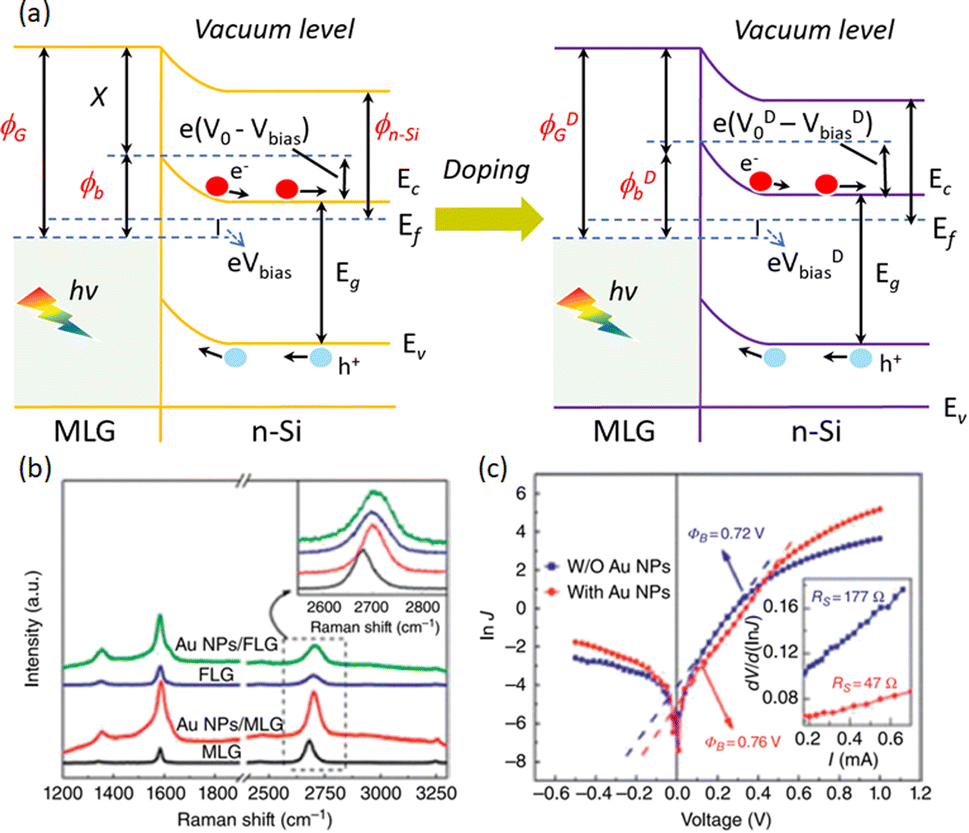 | ||
| Fig. 4 (a) The diagram of band structure and ϕwf of the MLG/Si interface prior to and following the doping process. (b) Raman spectroscopy results showing the spectra of MLG and FLG with and without the presence of Au NPs. (c) Dark J–V curves of the FLG/Si SCs with and without Au NPs. The inset presents the graphs of dV/d(lnJ) versus I, enabling the determination of the series resistance RS of cells. (b)–(d) have been reproduced from ref. 89 with permission from American Institute of Physics. | ||
Aside from increasing the number of layers, doping has been established as an effective method for reducing the sheet resistance of graphene. Different doping approaches using chemical doping have been successfully utilized. Heteroatom doping involves the substitution or bonding of atoms like oxygen, boron, nitrogen, phosphor, and sulfur, with carbon atoms in the graphene lattice. Nevertheless, dopants are chosen over heteroatom doping for application in G/Si SCs. Amongst different dopants, HNO3, SoCl2, and AuCl3 have shown promising results. Cui et al. found that SoCl2 is the most effective dopant to improve the PCE of SCs to 2.3% due to decreased sheet resistance.75 SoCl2 modified graphene also decreases sheet resistance from 735 to 405 Ω sq−1. Feng et al. with demonstrated a reduction in series resistance (Rs) of the SCs from 6.11 Ω cm2 to 4.07 Ω cm2 and an improvement in PCE from 2.9% to 4.35% after immersing the device in HNO3, along with VOC, JSC, FF enhancement to 495 mV, 17.22 mA cm−2 and 51%, respectively.72,85 Although chemical doping has shown promising results in reducing graphene resistance and SC efficiency, there is concern regarding the durability of the covalent functionalization of graphene. Degradation of the functionalization caused by the ambient air can result in a significant decrease in PV enhancement by up to 50%. However, doping by gold chloride (AuCl3) has demonstrated better environmental stability than other reported methods.86 The reduction of Au3+ to Au NPs by transferring charges from graphene results in p-doping of graphene, leading to substantial enhancements in conductivity. The sheet resistance by AuCl3-dopped MLG results in reducing sheet resistance and enhancing efficiency.73,87
In addition, doping with organic compounds can also improve the physical properties of graphene.90,91 For example, doping with trifluoromethanesulfonic amide (TFSA) resulted in an increase in the PCE of the G/Si device from was increased 1.9% to 8.6%, an increase in the JSC from 14.2 to 25.3 mA cm−2, and an increase in the VOC from 0.43 to 0.54 V, for doped and un-doped graphene, respectively.76 When TFSA is functionalized on monolayer graphene, it has been observed that the resistance decreases from 1200 to 300 Ω cm−2 without notable impact on transmittance. Most of these dopant’s p-dope the graphene, leading to a decrease in the sheet resistance of graphene by shifting the graphene Fermi level downward or increasing the ϕwf. Since graphene also behaves as a junction layer, the increase in the ϕwf has additional implications at the interface. The enhanced graphene ϕwf leads to an elevated SBH, thereby establishing a more robust built-in electric field and more efficient separation of carriers. As depicted in Fig. 4a, the rise in Voc following the doping process enhances the built-in potential Vo and the barrier height (ϕb). This adjustment aligns with the variance of the work function of MLG (ϕG) and the electron affinity of Si (χ).88 Chemical doping raises ϕG, promoting enhanced charge transfer and collection at the interface. Consequently, the enhancement brought about by doping in the G/Si SCs combines improvements in graphene sheet resistance and an elevated Schottky barrier height.
Taking into consideration the instability of chemical doping, it is not practical for the utilization of graphene/Si PV devices. Therefore, more reliable doping techniques are increasingly coveted, and researchers have recently commenced investigating alternative approaches including physical and light-induced doping. Some metals (metal’s EF lower than graphene’s EF) have been found to effectively p-dope graphene. The doping capacity of metal NPs is determined by their ϕwf, with metals possessing higher ϕwf demonstrating more effective graphene doping. Successful p-doping is indicated by a blue shift in the 2D Raman peak upon deposition of Au NPs (Fig. 4b).89 By optimizing the Au NPs size, the PCE of G/Si SCs was increased to 7.34%. Au/HNO3 co-doped graphene increases the efficiency to 10.20% by achieving a raised ϕwf and improved electrical conductivity of graphene. As depicted in Fig. 4c, the reduction in the series RS of Schottky diode, attributed to the introducing of Au NPs, not only results in a heightened FF but also enhanced Jsc.89 This outcome aligns with findings from previous studies on the effects of HNO3 doping. Similarly, the work shows a high efficiency of 10.69% with Au/TFSA co-doped graphene.90 NPs of another metal, Pt, with a high ϕwf, have also been demonstrated to enhance the PCE to 7% through the integration of physical doping using high ϕwf Pt NPs, improved absorption of SCs in the visible region due to plasmonic effect and the photo-induced doping. Approaches to providing holes or electrons to graphene by using P3HT or TiO2 film were used. The suitability of HUMO of P3HT and VB of Si creates favorable conditions for hole transport under light illumination, enhancing carrier concentration. On the other hand, holes were captured by the traps in TiO2 whereas the electrons were moved to graphene.
In addition, prolong stable of SCs play a signify role. TiOx material coated on graphene can remain or reduce the degradation of PCE of SCs. A PCE value of 12.95% was reached, with degradation of less than 10% after 1-month storage by coated TiO2 layer.91 Efficiency levels of 8.2% and 10.5% were achieved for TiOx/G/p-Si without PMMA and with antireflection (AR) coating of PMMA, respectively. Furthermore, no significant changes in performance were observed over a period of 10 days.92 GO is a multi-functional component for G/Si SCs. For example, GO layer functions as p-type dopant for graphene and also acts as an AR layer within SC. PCE of the G/GO/Si CSs maintained a consistent 10% level over a span of 20 days.79 Using GO as a passivation layer led to a significant improvement in the lifetime of carriers.93 Simultaneously, GO also functioned as a protective; however, its barrier characteristics were observed to diminish at elevated temperatures (400 °C) because of GO decomposition and alterations in its doping levels.93
6.2. Influence of light trapping in silicon
The planar Si plays a significant importance for light absorption and electro/hole pairs generation. Therefore, the enhanced absorption of Si leads to an improvement in efficiency. However, planar Si exhibits high reflection. This drawback of planar Si induces the reduction efficiency of SC due to absorption losses. Nevertheless, the integration of micro/nano structures on the silicon surface can substantially enhance the light absorption capacity owing to the pronounced light-trapping phenomenon. This phenomenon effectively diminishes the sunlight reflection from the surface of the junction, resulting in enhanced charge-collection efficiency. For instance, employing patterning in the form of Si nanowires can increase the distance traveled by incident solar radiation by a factor as substantial as 73.92,93Fig. 5a and b describe the cross-section of Si nanowires of 2 μm and 5 μm.92 The transmittance spectra show that both Si nanowires of 2 μm and 5 μm before etching exhibit low transmittance.92 It is evident that correlated to planar Si, nanowires exhibit decreased transmission indicating strong light trapping. Similarly, in the case of G/Si SCs, texturing Si into structures such as pillars, nanowires, pyramids, etc. has been employed to minimize light reflection and enhance light absorption. These non-planar features redirect the incident light back into the Si rather than allowing it to transmit through the Si, leading to improved absorption through light trapping and subsequently boosting the overall PCE. Fan et al. fabricated Si NWs through metal-assisted etching method.94 The G/Si NWs SJ demonstrated higher absorption contrasted to the graphene/planar Si junction leading to the enhancing efficiency of up to 2.865% because the Si NWs contribute an immediate pathway to the overall improvement in performance due to direct and fast pathway of electron–hole collection as light trapped on the planar junction. Feng et al. implemented the pillar to enhance light absorption using photolithography and inductive coupled plasma (Fig. 6).72 The result implies that the Si pillar exhibits more absorption correlated with planar Si. The absorption intensity is strongly affected by pillar height and achieves the highest absorption with 900 nm pillar height. The PCE of G/Si pillar devices was measured to be 1.96% (which could be further enhanced to 3.55% by HNO3 doping), surpassing that of G/planar-Si SCs (1.65%). Xie et al. prepared the Si hole array (SiHA) using photolithography and reaction ion etching (RIE).95 The surface of SiHA displayed a smooth texture, validating the presence of minimal surface recombination velocity. As illustrated in Fig. 7, the light absorption of SiHA intensified as the depth of the holes increased, underscoring its heightened light-trapping capabilities.94,95 Through the mixture of light trapping in SiHA and the utilization of AuCl3 for graphene doping, researchers achieved a high PCE of 10.40%.94,95 These devices indicated remarkable stability, maintaining their increased efficiency even after being stored in ambient air for about 3 months.
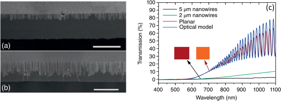 | ||
| Fig. 5 Tilted cross-sectional SEM images visuals portraying (a) arrays of nanowires measuring 2 μm and (b) arrays of nanowires measuring 5 μm. Scale bars are 10 μm for both images. In addition, (c) transmission spectra of thin Si structures are provided for the comparison: prior to etching (red), subsequent to etching into 2 μm (green), and following etching into 5 μm (black) nanowires. (a)–(c) have been reproduced from ref. 92 with permission from American Chemical Society. | ||
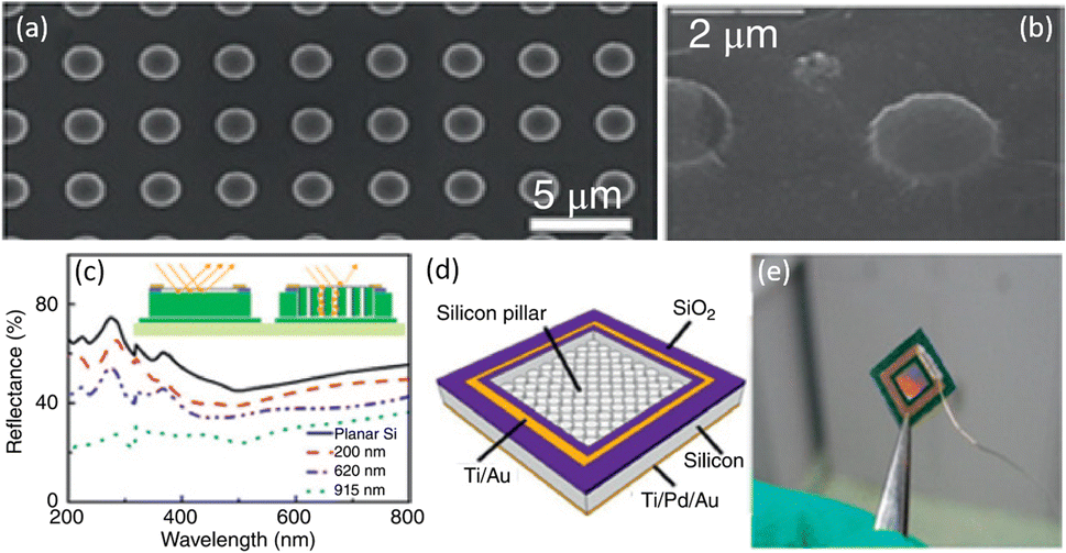 | ||
| Fig. 6 SEM image of Si pillar without (a) and with coated graphene (b), (c) the reflectance spectra of Si pillars with different pillar height and planar Si substrate. Inset presents the principle of antireflective effect of Si pillar substrate. (d) Schematic presentation of a G/Si pillar SB-SCs. (e) Photograph of a G/Si pillar SC with junction area of 0.09 cm2. (a)–(e) have been reproduced from 72 with permission from American Institute of Physics. | ||
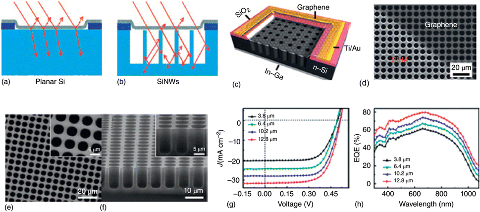 | ||
| Fig. 7 (a) Schematics diagrams of G/planar Si, (b) G/Si NW junctions. (a) and (b) have been reproduced from ref. 94 with permission from American Chemical Society. (c) Schematic presentation of the G/Si HA SB-SCs, (d) top-view SEM image of the G/Si HA device. The area included by graphene films shows darker contrast in the SEM image. (e) Top-view and (f) cross-sectional view SEM images of the as-prepared SiHA. Insets present the enlarged SEM images, (g) PV characteristics, and (h) EQE spectra of the G/Si HA SB-SCs with various hole depths. (c)–(h) have been reproduced from ref. 95 with permission from Royal Society of Chemistry. | ||
6.3. Antireflection coating
Antireflection coating (ARC) is a method that uses a dielectric layer such as SiO2, TiO2 to enhance the performance of G/Si solar cells by reducing the reflection of incident light at the surface of the Si. This layer is designed to optimize and minimize the loss of incoming photons owing to reflection, thereby increasing the amount of light that can be absorbed by the solar cells (Fig. 8a).96 In the case of G/Si structures with an ARC, the resulting stack consists of four layers: air/ARC/G/Si. Fig. 8b indicates the refractive index of some of ARC candidate materials.97 TiO2 is a promising candidate for ARC due to its refractive index. However, the integration of TiO2 film and graphene surface depends on the fabrication methods.96 The physical deposition method with high energy can destroy the graphene while solution methods still maintain the pristine graphene. Instead, Shi et al.97 prepared TiO2 film by sol–gel method on G/Si SCs, as presented in Fig. 8a.96 The results show that the reflectance was reduced to 10% (with TiO2 film) compared to without TiO2, as indicated in Fig. 8c.97 Fig. 8d compared the J–V characteristics of SCs with un-doped, HNO3-doped, and TiO2 coated on HNO3-doped.97 The J–V characteristics show that the PCE of SCs improve when SCs were doped and combined doping and coating ARC layer refractive polymers, like PMMA (n = 1.5), can be used as RAC for G/Si SCs because they are highly transparent to visible light. Despite having a low refractive index compared to inorganic ARC materials, it has benefits including being very transparent to visible light, light in weight, bendable, and flexible. Additionally, PMMA is commonly employed as a foundation layer during the transfer of graphene. By repurposing PMMA as an ARC, the need for removing PMMA subsequent to the graphene transfer is obviated, simplifying the device production process. The performance of G/Si SCs was significantly improved by utilizing PMMA-coated graphene films contrasted to bare G/Si SCs that underwent PMMA elimination. Fig. 8e contrasts the reflectance spectra of PMMA eliminated G/Si and PMMA-G/Si devices, indicating that the PMMA-G/Si devices exhibit higher absorption capabilities.98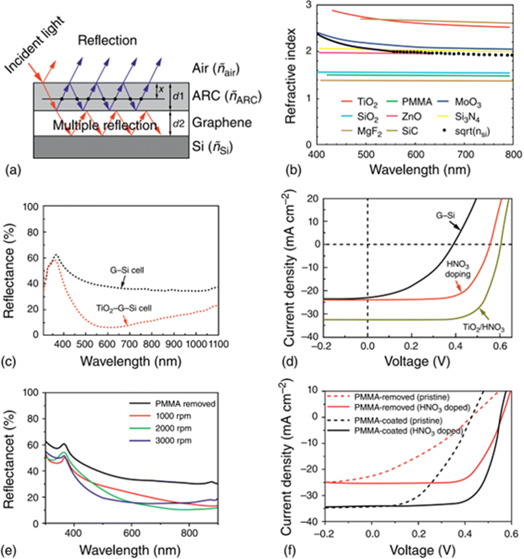 | ||
| Fig. 8 (a) Patterning of the Si substrate, (b) relationship between refractive index and wavelength for certain ARC materials. (a) and (b) have been reproduced from ref. 96 with permission from Royal Society of Chemistry. (c) Light reflection spectra of a g/Si SCs prior to (black) and following (red) the application of a TiO2 colloid coating, illustrating antireflection effect, (d) J–V characteristics of an as-deposited G/Si SCs, after HNO3 vapor doping, and after TiO2 coating (together with HNO3 doping), respectively. (c) and (d) Have been reproduced from ref. 97 with permission from American Chemical Society. (e) Reflectance spectra of PMMA-extracted and PMMA-grown graphene samples on quartz slides, (f) J–V curves of PMMA-removed and PMMA-coated (2000 rpm) G/Si SCs before and after HNO3 doping. (e) and (f) Have been reproduced from ref. 98 with permission from Royal Society of Chemistry. | ||
Fig. 8f demonstrates the JSC, FF, and PCE of PMMA extracted-G/Si and PMMA-G/Si SCs of 22.61 mA cm−2, 32.22%, 3.12%, and 33.64 mA cm−2, 45.56%, 6.55%, respectively.99 In particular, the PCE of HNO3-doped PMMA-G/Si SCs up to 13.34%. It is noteworthy that the structure of PMMA was not affected by the HNO3 doping, making the doping procedure of PMMA coated graphene convenient. Ding et al.100 utilized double layered MgF2/ZnS coating on G/Si SCs, serving a dual intention. Firstly, for Si SCs operating in the range of 380 to 1100 nm, ZnS and MgF2 have higher (n = 2.5) and lower (n = 1.4) refractive indices, respectively. Therefore, the MgF2/ZnS double layer served as an effective ARC. Secondly, by adjusting the thickness of ZnS and MgF2, different colors could be transmitted to G/Si SCs. The color tuning process for G/Si SCs was easy due to the transparent nature of graphene. Fig. 9 depicts the display, visuals, and CIE chromaticity coordinates of seven colors for G/Si SCs with DL-MgF2/ZnS films.100
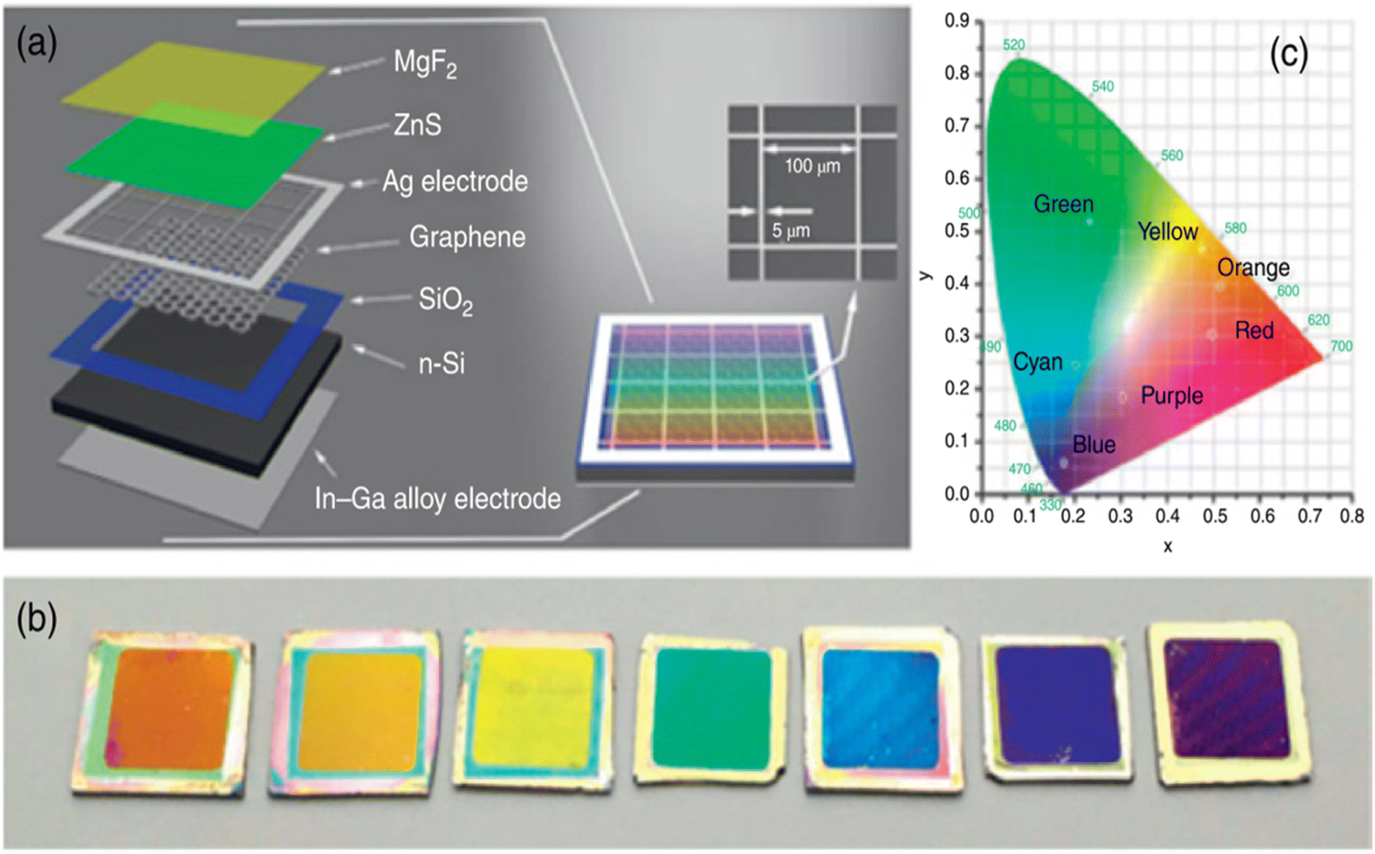 | ||
| Fig. 9 G/Si SB-SCs with (a) schematic presentation of the color device, (b) photographs of device area: 1 cm2 with various colors, and (c) coordinates of seven colors in CIE chromaticity. (a) and (b) Has been reproduced from ref. 99 with permission Elsevier. | ||
Fig. 10 illustrates the reflectance spectra of different colored MgF2/ZnS coated G/Si SCs.99 It is evident that the absorption was enhanced correlated to pristine G/Si SCs. Comparable trends were seen for the EQE spectra. Remarkably, the multi-color G/Si SCs achieved a high PCE of 10.7–13.2%.99 By utilizing an enhanced MgF2/ZnS antireflection layer, the PCE of the device reached an impressive value of 14.6%.99
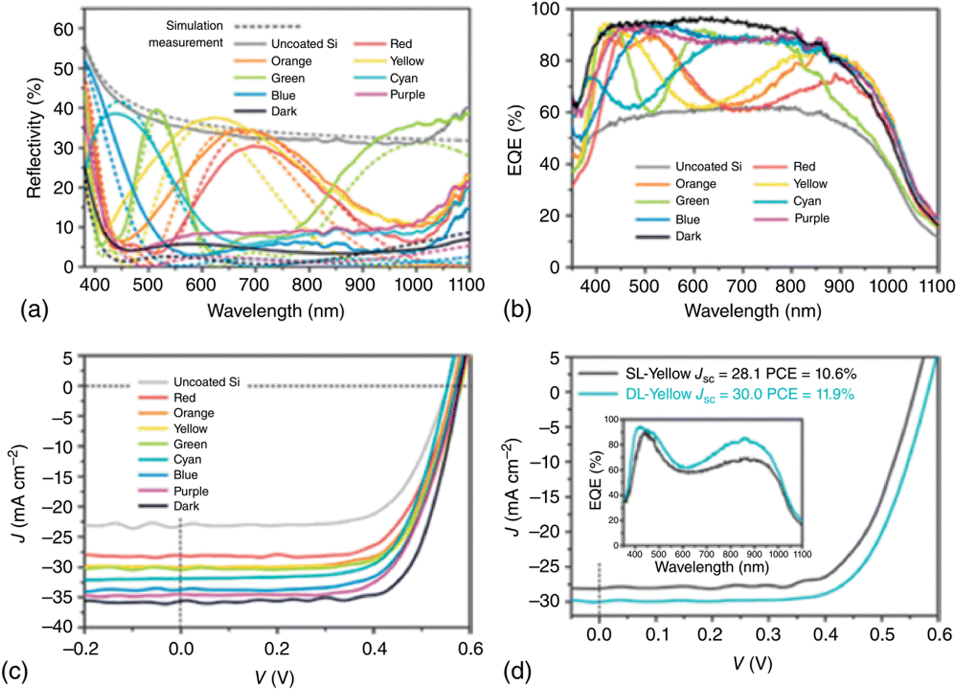 | ||
| Fig. 10 (a) Modeled (dash lines) and observed (solid lines) reflection spectra of DL-MgF2/ZnS-coated G/Si heterojunction SCs (b) EQE spectra of the uncoated and G/Si SCs with various structural colors, (c) J–V spectra of the devices with various structural colors. J–V spectra of the devices without coating and with enhanced anti-reflection coating were also indicated for comparison, (d) contrast of the J–V and EQE (inset) among SL-ZnS-coated and DL-MgF2/ZnS-coated G/Si devices. (a)–(d) Have been reproduced from ref. 99 with permission from Elsevier. | ||
6.4. Influence of engineering
Despite numerous methods being used to enhance G/Si devices, their performance is still inferior to that of Si p–n SB-SCs used in commercial applications. This discrepancy primarily arises from the diminished built-in electric field in the SJ, which cannot effectively suppress carrier combinations along the interface. By overwhelming obstacle carriers (electron in n-Si) via inserting an interfacial barrier layer between graphene and Si, recombining electron/hole pairs can prevent and ought to support the transfer of holes to graphene. However, the types of materials and the thicknesses of the layers are is a signify to the extensive study. Some thin film materials such as SiO2, h-BN, MoS2, MoO3, and P3HT have been utilized.101–105 If the layer is very thick, the ohmic inefficiencies can appear. On the other hand, the layer is too thin and may fail to block majority carriers' transport. Therefore, optimizing the dimension of the barrier layer is necessary to strike a balance between reducing carrier recombination and minimizing ohmic losses. Studies have shown that oxide layers with a thickness of lower than 2 nm can effectively passivate the interface, leading to increased VOC and FF. By selecting the optimal oxide thickness (1.5 nm), a PCE of 12.4% was achieved through chemical doping. This efficiency further increased to 15.6% following the implementation of a TiO2 ARC.101,102 The thickness of ultra-thin SiO2, however, is difficult to adjust because it depends on the crystal orientation and external factors.Recently, the insulating material of h-BN, an appealing choice as a barrier layer for G/Si SCs due to high transparency, dangling bond-free surface, and proper band alignment with n-Si substrate.101 Fig. 11 presents the band diagram of G/h-BN/Si SCs, highlighting the effects of h-BN insertion.101 It's clear that compared to a basic G/Si interface, the introduction h-BN creates a substantial barrier that impedes electron transfer at the interface.102 However, it simultaneously enables easy transport of holes from Si to graphene. Through the incorporation of the BN layer, PCE of the G/Si SCs attained 10.93%, which indicated a 15% efficient enhancement contrasted to the reference device.
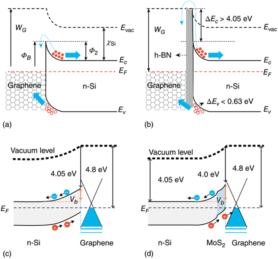 | ||
| Fig. 11 Energy band diagrams of the G/Si SB-SCs (a) without and (b) with an h-BN electron blocking layer. (a) and (b) have been reproduced from ref. 102 with permission from Elsevier Presentations of band diagrams for the SCs. The PV procedures (c) in the graphene/n-Si and (d) in the graphene/MoS2/n-Si SCs are indicated. (c) and d have been reproduced from ref. 101 with permission from Royal Society of Chemistry. | ||
Semiconductor layers with thickness (∼50 nm) can be employed as barrier layers, offering a more convenient processing approach compared to insulators which require decreased thickness. MoS2 thin film grown by different methods has been utilized as an interfacial barrier layer to improve PCE of SCs. The insertion of MoS2 layer introduces a shift in the EF, causing the lowest part of the CB and the top of VB of the MoS2 layer at the interface of graphene to move upward, as shown in Fig. 11a–d.101 This creates an energy barrier at the interface between MoS2 and n-Si and enhances the entire energy barrier among graphene and n-Si. The additional energy barrier provided by the MoS2 layer effectively blocks the photogenerated electrons in the Si, serving as an efficient electron-blocking layer. Alike band bending at the interface of the semiconductor barrier layer/n-Si interface has been noted in the cause of WO3/n-Si structures.101 The substantial disparity in energy levels between the EF of WO3 and Si prompts a marked transfer of charges from Si, leading to a pronounced upward bending of the band at the interface of WO3 and Si. Consequently, the built-in field (Vbi) of the G/Si SCs is improved inserting the WO3 interlayer, leading to a notable improvement in PCE from 3.99% in G/Si SCs to 10.59%. Utilizing MoO3 layers also contributed to elevating the PCE to 12.2% as a result of the significant ϕwf discrepancy in MoO3, leading to the spontaneous injection of holes from the MoO3 layer to Si.101 As a result of this hole injection process, a hole inversion layer is created at the surface of Si, generating a robust built-in electric field. This process effectively curbs recombination. Through additional device optimization steps involving graphene doping and the application of polymer anti-reflection coating, a high PCE of 12.2% was accomplished.
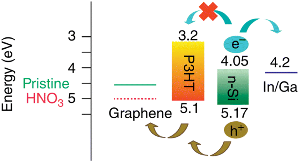
Organic semiconductors, P3HT also act as a hole transport layer and block the electron to reduce the recombination. Fig. 12 illustrates the band of P3HT and Si that LUMO and HUMO of P3HT are 3.2 and 5.1 eV, while the lowest conduction band and highest valence band are 4.05 and 5.17 eV.106 This substantial offset allows the transport of holes, but it hinders the electrons. Optimized graphene/P3HT/Si NW array and graphene/P3HT/Si NH array devices achieved power conversion efficiencies of 9.94% and 10.34%, respectively.
 | ||
| Fig. 12 Band diagram schematic of hybrid SCs. Figure has been reproduced from ref. 106 with permission from American Chemical Society. | ||
A significant interaction at the interface between Si and MoO3 layers has been noted, resulting in the remarkable attainment of PCE value of 12.2%. A substantial work ϕwf disparity was observed in MoO3, leading to the spontaneous injection of holes from the MoO3 layer to Si. This hole injection mechanism instigates the formation of a hole inversion layer on the Si surface and triggers the establishment of potent built-in electric field, effectively suppressing the recombination. Through additional device optimization steps involving graphene doping and the application of polymer anti-reflection coating, a high-PCE of 12.2% was accomplished.
6.5. Surface passivation
Surface passivation is another strategy to raise the PCE of SCs.107–109 As a result of the numerous dangling bonds on the Si surface, numerous surface states serve as recombination hubs. Recombination has a significant impact on the performance of G/Si and PV devices. The diffusion channel of the carrier can be improved to prevent recombination by dangling bond reduction on the Si surfaces. Various chemical entities, including hydrogen (H−), methyl (CH3−), and oxide (SiOx), have the potential to serve as passivation agents for Si surface.110,111 Hydrogen-passivated Si surfaces have garnered significant attention in the research literature due to their remarkable ability to passivated effectively (causing a substantial reduction in surface states by multiple orders of magnitude) and exhibit an exceptionally low surface recombination velocity.110,112,113 Among them, oxide SiOx shows the most chemical stability while H− termination exhibits low chemical stability and is incompatible with graphene leading to Schottky barrier decrease.114 However, the compatibility of CH3− group leads to the increase in the Schottky that they are better for SC efficiency improvement. The result shows that passivation on Si surface exhibits the PCE of 1.41%, 1.76%, and 4.42% with H−, CH3−, and oxide passivation, respectively.114 Other passivation layers such as modified SiO2, Al2O3, HfO2, GO, P3HT, and SiNx are also used to improve the SC efficiency.87,115–1176.6. Influence of encapsulation
Although the integrated G/Si heterojunctions in solar cells have achieved a lot of good results. However, another problem in the design and produce G/Si solar cells is also extremely important, that related to encapsulation of device to avoid and protect individual solar cells modules from various environmental factors and mechanical stress by enclosing them within protective materials and structures. In a report of Matacena et al. has used HNO3 as a doping source to improve the performance of G/Si heterojunction solar cells.118 Simultaneously, the author has also been compared with/without encapsulated by ethylene-vinyl acetate (EVA). The results from C–V analysis are confirm that encapsulation avoids the fading of HNO3 beneficial effects while it did not worse cells performance. In another innovation, Kim et al. has applied a protective layer for silver nanowires (Ag NWs) by graphene.119 In this work, the author designed the encapsulated graphene/Ag NWs/graphene for Schottky-type Si heterojunction solar cells. With this structure, the author has obtained a highest PCE of 3.51%, and it lost only 6.4% of its original PCE value after 30 days by employing the encapsulation layer, much less compared to the solar cells without the encapsulation. Since, G/Si solar cells encapsulation is vital part of PV module manufacturing, aimed at protecting the solar cells and ensuring the long-term performance and reliability of solar panels. Proper encapsulation helps extend the lifespan of solar modules and allows them to operate efficiently in a wide range of environment.7. Conclusion, challenges, and perspectives
In general, owing to its exclusive characteristics, graphene has been recognized as an outstanding material for various solar energy harvesting devices. Its unique characteristics hold the promise of being efficient, environment-friendly, and inexpensive after a decade of devoted research and in-depth scientific discoveries. But there are still many perspectives and challenges ahead.With its numerous advantages as a component of an SC, it possesses some limitations that can hinder it from being considered one of the best materials for an efficient SC. Graphene is widely regarded as a pivotal conductor of electricity, but it lacks a band gap in its molecular orbital structure, a shortcoming that researchers have been working to rectify over the years. Once this limitation is overcome, graphene can serve as an exceptionally efficient anode in virtually any type of SCs. Another challenge associated with graphene is its susceptibility to oxidation in oxidative environments. This oxidation leads to structural changes that subsequently impact its chemical properties. Efforts are underway to develop strategies to mitigate the effects of oxidation and enhance graphene's stability. Despite these challenges, researchers are actively working to overcome these limitations and harness the full potential of graphene for SC applications. The chemical alterations and structural changes that can occur in graphene pose a significant challenge when considering large-scale energy production. Moreover, graphene exhibits some toxic properties, which is a matter that requires to be carefully examined in its development. Secondary cells typically have two electrodes, whereas SCs have only one electrode. This creates two main issues: changes in the ϕwf value and the direction of electron flow. The electron flow system in a SC with only one electrode is complex, and maintaining the integrity of the entire process is a significant task. Researchers have attempted to modify the ϕwf to address this challenge but altering the ϕwf of a specific material is a difficult endeavor. Aside from this persisting issue, it has been discovered that depositing graphene electrodes into the solar setup has proven to be a difficult task. The bottom of a graphene electrode is deposited on a substrate material (usually glass or elastomers) that acts as the foundation makes up for the SCs.120 Owing to the poor dispersion properties of graphene, water is used as an appropriate solvent during this deposition process. However, various organic solvents are being tested to replace water in order to achieve a higher degree of dispersion. In typical graphene-induced SCs, when integrated into an n-Si SB-SCs with AM 1.5 illumination, it demonstrates a PCE of 8.6%. This value can be increased 4.5 times when doping the SC material. To achieve this, graphene is doped with ionic liquids such as bistriflimide, bis(trifluoromethanesulfonyl)amide, and others.121–123 The doping process alters the chemical potential of graphene, leading to an increased carrier density, ultimately elevating the built-in potential of the SCs. This, in turn, enables a longer cell lifespan compared to traditional SCs. Recent approaches in optimizing G/Si SB-SCs were developed. These strategies can be divided into optimizing (i) the ϕwf and conductivity of graphene, (ii) Si's reflectivity, and (iii) modifying the G/Si interface. Through the implementation of these strategies, the PCE has risen from 1.5% to 15.8% in less than 10 years. Despite the fast advancements in this area, there are remaining matters that require further attention.
Firstly, various strategies have been explored to improve the PCE of SCs including passivation and band-engineering of the G/Si interface, insertion of an antireflection layer or nano-micro structures in enhancing the light harvest, the control of the number of graphene layers, and the chemical doping of graphene which has been confirmed to be the most efficient method for optimizing SC performance. Despite the introduction of numerous doping dopants, the durability of SCs remains a challenging issue due to the unsteadiness of the doping process. An increased stable single-walled carbon nanotube (SWa-CNT)/Si SCs with a PCE greater than 11% after 10 months of ambient encounter was demonstrated.124 By inserting a GO interlayer to develop a G/Si interface, new structure of G/GO/Si SC occupies 95% of its original level after one week of storage in the open air.125 Similarly, an Al2O3 interlayer was inserted by Rehman et al.115 among the graphene and Si to inhibit the surface charge recombination at the interface, and their SC maintained its efficiency without degradation even after 9 months of exposure to ambient air. Initially, chemical doping of graphene led to a significant deterioration of G/Si SCs. Recently, GO demonstrated some PCE durability where Yavuz et al. published the degradation in PCE less than 1% after 3 weeks.79,126 Nevertheless, more research into the stability under various parameters, such as humidity and temperature, is needed. Moreover, alternative materials such as a CNT-oxide-Si cell with a PDMS anti-reflective coating were employed to reveal a small drop in efficiency from 10.9% to 9.1% in air over 20 days. Thus, materials with high durability, like CNTs, can be utilized to ensure the stability of a SC. Investigating new SC structures, such as introducing an interlayer to engineer G/Si interface to create a metal–insulator–semiconductor (MIS) structure, could also be a vital direction in this field.
Secondly, although the PCE of G/Si SCs managed 15.8% in a few years, it still falls short of the PCE achieved by commercially available Si–p–n junction SCs. One of the limitations contributing to this is the decreased electrical conductivity and ϕwf of graphene. As a result, the energetic region of current studies involving G/Si SCs is relatively small (<10 mm2). Researchers demonstrated the device performance in various device areas from 4 to 100 mm2. Interestingly, the PCE decreased from 10.56% to 3.62%, with an increase in the device area. This reduction in efficiency can be attributed to series resistance, which influences performance of SCs at larger scales. This result underscores the direct relationship between the energetic region of a SC and its overall behavior.127 Furthermore, it has been reported in another study that the PCE of G/Si SCs lowered from 14.5% to 10.6% as the active region raised from 4.7 mm2 to 14.5 mm2.97 However, through interface engineering, it has been demonstrated that G/Si SCs can reach a PCE over 7% with a device region of 0.09 cm2.125 It is essential to raise the active area to a minimum of 0.1 cm2 for further improvement. Due to high sheet resistance of the graphene layer, the collection efficiency of photogenerated charge carriers would be decreased with a larger size of the device's active area. A grid electrode has been introduced to the traditional window-based device structure to reduce the resistance of graphene layer.128 This grid electrode design facilitates low-resistance contact with the graphene layer and enhances carrier collection efficiency. Therefore, employing a fine metal electrode design on the front side is essential to favor carrier collection throughout the entire device region. Another significant matter is the long-term durability of these G/Si SCs. With the passage of time, the performance of these SCs begins to deteriorate, particularly after the doping process. A number of researchers have studied the durability of G/Si SCs during storage and attempted to mitigate the deterioration. Xie et al.95 noted outcomes after various time intervals, indicating that the PCE of G/Si SCs decreased from 10.40% to 7.42% within 3 months.
Third, graphene is commonly moved on a Si substrate to create an SJ. However, graphene is fragile, and the remaining copper particles may stay on the graphene film after wet etching.129,130 These contaminants at the G/Si interface can act as short-circuit channels, resulting in current loss. As expected, the leakage current becomes more prominent as the device area increases. Therefore, the increased area of graphene is an important parameter affecting collection efficiency. To address this issue, advanced manufacturing and transfer skills must be addressed to reduce the flaws and contaminants encountered during the wet transfer method. Additionally, an alternative approach involves directly growing graphene on the semiconductor surface, resulting in a more uniform graphene with fewer structural defects.131
On the other hand, G/Si PVCs are progressing in large-scale integration, offering high-efficiency and sustained solar technologies.84 Nevertheless, the performance of G/n-Si single-junction cells falls short compared with that of p–n junction of SCs due to some main causes, such as low Schottky barrier height, transfer-based SC design, and high lateral resistivity of graphene. The interfacial barrier height of G/n-Si SCs is ϕG − ϕSBH = ϕG − χn-Si = 0.65 eV which is lower than the Si energy bandgap (1.1 eV at 300 K). The G/Si SC designs evolved by moving graphene onto the Si substrates through a polymer-film-based chemical-transfer procedure. This process can cause defect centers, exacerbating interfacial carrier recombination and ultimately lowering the PV performance. The mobility of charge carriers of layer graphene grown by CVD is better than other methods. Nevertheless, a single graphene layer has a higher sheet resistance (100–100 Ω−1) than the solar-grade doped Si (50–100 Ω−1) of the p–n junction SCs.132 Such high lateral resistivity of graphene films results in inefficient losses such as increased RS and decreased fill factors in G/Si PV heterojunction cells. Several approaches to overcoming the challenges of G/Si PV devices have been explained.84 The following part outlines strategies for tuning the interface utilizing suitable interlayers and modulating the functionality of graphene, all aimed at reaching highly efficient and robust G/Si SCs.
Graphene's impact on the field of solar energy harvesting devices is not limited to revolutionizing renewable energy assets. It is also a promising material for smart energy generation and storage devices. Nevertheless, conventional energy generators are incapable of providing responses to environmental changes and traditional energy storage devices lack functionalities other than providing electricity, posing challenges. However, graphene owing to its microscopic structure modification and exceptional physicochemical properties offers potential solutions to these issues. Thus, intelligent energy generation and storage and smart electric devices that can engage with receptive to external stimuli are becoming increasingly important and highly demanded. Recently, the key advances that involve the integration of graphene into smart energy generation and storage systems were systematically reviewed by Ye et al.133 In the context of smart energy generation, the authors discussed graphene-derived electric generators that can harvest electricity in response to external stimuli, such as flowing liquid, moisture, pressure force, friction, and heat. These advanced energy storage solutions exhibit remarkable features such as wearability, deformability, printability, responsiveness to stimuli, integration capabilities, miniaturization, and self-healing properties, showcasing the exciting possibilities enabled by graphene in the realm of energy storage.
Industrial production has been extremely high with a massive global demand for graphene-based commercial products. In PVs, graphene has been discovered as an electrode in SC technologies thanks to its brilliant properties. Recent advancements in G/Si-based (SB-SCs) have received considerable attention. With the noble continued efforts of researchers, the PCE for G/Si SCs has dramatically increased from 1.65% to 15%, which is comparable to that of metal halide perovskite cells with the highest efficiency of 20–22%.134 However, there is a great opportunity for enhancement in the behavior of G/Si SCs. To improve the overall PCE of G/Si SCs, chemical doping of graphene, interfacial layer utilization, and anti-reflection coatings have played significant roles. The surface recombination in influencing FF was expanded with prominence on the passivation approach and the use of a thin hole transport interlayer. All parameters such as JSC, VOC, and FF, eventually establish the PCE of certain G/Si SCs. In perceptions, G/Si appears to offer new utilizations for future-generation SCs. Despite its fast progress, there are challenges and limitations to its implementation on a commercial scale. One of the major challenges lies in achieving continuous graphene growth with excellent material quality. Additionally, the environmental durability of G/Si SCs is a concern. However, recent advancements suggest that graphene-based electronics combined with Si can lead to high-efficiency SCs with commercial viability. Therefore, G/Si heterostructure systems demonstrate industrial potential, as efforts are being made to reduce costs and capitalize on their lightweight nature and corrosion resistance, making them an ideal material for PVs. Several companies and research institutes are now emphasizing on graphene chemistry R&D to enhance the efficiency and production of induced graphene in SCs. Following the successful implementation of graphene electrodes in the SC, various other electronic entities are exploring improving graphene in their machinery in order to reach the same level of efficiency in those sectors. The automotive industry can become more environmentally friendly by incorporating SCs, which enhance the speed and range of solar cars. In conclusion, graphene-induced SCs are considered one of the most significant inventions of this decade, capturing the attention and driving the development of the global scientific community. Furthermore, scientists are actively working towards enhancing the efficiency of graphene-based SCs to maximize energy harnessing. By promoting solar energy, graphene holds a key role in facilitating sustainable, clean, and environmentally friendly energy productions and utilization worldwide (Fig. 13). Importantly, graphene's success extends beyond SCs to encompass various notable applications, including sensors, photodetectors, and smart energy generation and storage devices.
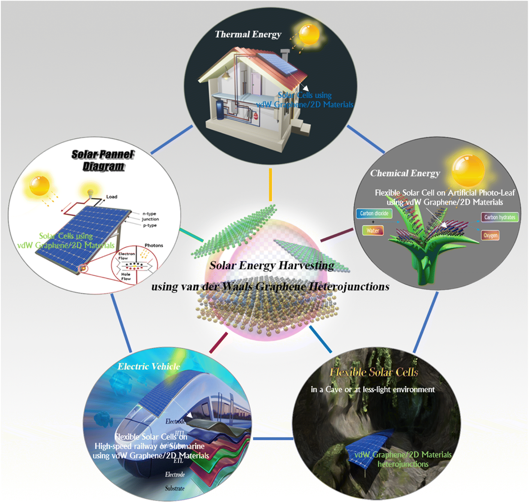 | ||
| Fig. 13 The promising prospects of van der Waals graphene heterojunctions integrated into the solar energy harvesting. | ||
Author contributions
Top Khac Le: investigation, writing – original draft. The-Hung Mai: writing – original draft. Muhammad Aamir Iqbal: writing – original draft. Dimitra Vernardou: writing – original draft. Van Duong Dao: writing – original draft. Vinoth Kumar Ponnusamy: investigation, writing – original draft. Chandra Sekhar Rout: investigation, writing – original draft. Phuong V. Pham: resources, project administration, funding acquisition, conceptualization, methodology, investigation, writing – original draft, writing – review & editing.Conflicts of interest
The authors declare that they have no known competing financial interests or personal relationships that could have appeared to influence the work reported in this paper.Acknowledgements
The authors acknowledge the supports from the National Science and Technology Council, Taiwan (Grant No. NSTC-112-2112-M-110-004-MY3), the Research Center for Precision Environmental Medicine, Kaohsiung Medical University, Kaohsiung, Taiwan from The Featured Areas Research Center Program within the framework of the Higher Education Sprout Project by the Ministry of Education (MOE) in Taiwan and by Kaohsiung Medical University Research Center Grant (KMUTC112A01), and the grant MOST-110-2113-M-037-009- from the Ministry of Science and Technology, Taiwan.References
- B. Parida, S. Yoon, S. M. Jeong, J. S. Cho, J. K. Kim and D. W. Kang, Sol. Energy Mater. Sol. Cells, 2020, 204, 110212 CrossRef CAS.
- K. Yoshikawa, H. Kawasaki, W. Yoshida, T. Irie, K. Konishi, K. Nakano, T. Uto, D. Adachi, M. Kanematsu, H. Uzu and K. Yamamoto, Nat. Energy, 2017, 2, 17032 CrossRef CAS.
- M. Nakamura, K. Yamaguchi, Y. Kimoto, Y. Yasaki, T. Kato and H. Sugimoto, IEEE J. Photovoltaics, 2019, 9, 1863–1867 Search PubMed.
- N. Yan, C. Zhao, S. You, Y. Zhang and W. Li, Chin. Chem. Lett., 2020, 31, 643–653 CrossRef CAS.
- W. Shi and X. Ma, Coatings, 2018, 8, 2 CrossRef.
- V. P. Pham and G. Y. Yeom, Adv. Mater., 2016, 28, 9024–9059 CrossRef CAS.
- P. V. Pham, S. Chanakya Bodepudi, K. Shehzad, Y. Liu, Y. Xu, B. Yu and X. Duan, Chem. Rev., 2022, 122, 6514–6613 CrossRef CAS PubMed.
- C. H. Lee, G. H. Lee, A. M. Van DerZande, W. Chen, Y. Li, M. Han, X. Cui, G. Arefe, C. Nuckolls, T. F. Heinz, J. Guo, J. Hone and P. Kim, Nat. Nanotechnol., 2014, 9, 676–681 CrossRef CAS PubMed.
- M. Shanmugam, R. Jacobs-Gedrim, E. S. Song and B. Yu, Nanoscale, 2014, 6, 12682–12689 RSC.
- T. Saga, NPG Asia Mater., 2010, 2, 96–102 CrossRef.
- K. S. Novoselov, A. K. Geim, S. VMorozov, D. Jiang, Y. Zhang, S. V. Dubonos, I. V. Grigorieva and A. A. Firsov, Science, 2004, 306, 666–669 CrossRef CAS PubMed.
- A. K. Geim and K. S. Novoselov, Nat. Mater., 2007, 6, 183–191 CrossRef CAS PubMed.
- A. A. Balandin, Nat. Mater., 2011, 10, 569–581 CrossRef CAS PubMed.
- T. Mahmoudi, Y. Wang and Y. B. Hahn, Nano Energy, 2018, 47, 51–65 CrossRef CAS.
- Q. Zheng, Z. Li, J. Yang and J. K. Kim, Prog. Mater. Sci., 2014, 64, 200–247 CrossRef CAS.
- A. DiBartolomeo, Phys. Rep., 2016, 606, 1–58 CrossRef CAS.
- G. Luongo, A. Grillo, F. Giubileo, L. Iemmo, M. Lukosius, C. A. Chavarin, C. Wenger and A. DiBartolomeo, Nanomaterials, 2019, 9, 659 CrossRef CAS PubMed.
- B. Partoens and F. M. Peeters, Phys. Rev. B: Condens. Matter Mater. Phys., 2006, 74, 075404 CrossRef.
- P. V. Pham, The New Etching Technologies of Graphene Surfaces, IntechOpen, 2020, DOI:10.5772/intechopen.92627.
- P. Pham, P. Goel, S. Kumar and K. Yadav, 21st Century Surface Science - A Handbook, IntechOpen, 2020, DOI:10.5772/intechopen.87891.
- P. V. Pham, 21st Century Nanostructured Materials - Physics, Chemistry, Classification, and Emerging Applications in Industry, Biomedicine, and Agriculture, IntechOpen, 2022, DOI:10.5772/intechopen.94802.
- K. A. A. Min-Dianey, T. K. Le, J. R. Choi and P. VPham, Nanomaterials, 2021, 11, 816 CrossRef CAS PubMed.
- K. A. A. Min-Dianey, T. K. Le, A. Qadir, N. L. P. M’bouana, M. Malik, S. W. Kim, J. R. Choi and P. V. Pham, Nanomaterials, 2021, 11, 2934 CrossRef CAS PubMed.
- U. Farooq, K. A. A. Min-Dianey, P. Rajagopalan, M. Malik, D. Mani Kongnine, J. R. Choi and P. VPham, Nanomaterials, 2022, 12, 712 CrossRef CAS PubMed.
- M. A. Iqbal, M. Malik, W. Shahid, W. Ahmad, K. A. A. Min-Dianey, P. V. Pham, Plasmonic 2D Materials: Overview, Advancements, Future Prospects and Functional Applications, IntechOpen, 2021, DOI:10.5772/intechopen.101580.
- P. V. Pham, Atmospheric Pressure Chemical Vapor Deposition of Graphene, IntechOpen, 2018, DOI:10.5772/intechopen.81293.
- V. P. Pham, Direct Growth of Graphene on Flexible Substrates Toward Flexible Electronics: A Promising Perspective, IntechOpen, London, UK, 2017 Search PubMed.
- V. P. Pham, H. S. Jang, D. Whang and J. Y. Choi, Chem. Soc. Rev., 2017, 46, 6276–6300 RSC.
- P. V. Pham, R. Soc. Open Sci., 2018, 5, 1–6 Search PubMed.
- A. Qadir, T. K. Le, M. Malik, K. Aniya, A. Min-Dianey, I. Saeed, Y. Yu, J. R. Choi and P. VPham, RSC Adv., 2021, 11, 23860–23880 RSC.
- M. Malik, M. A. Iqbal, J. R. Choi and P. V. Pham, Front. Chem., 2022, 10, 905404 CrossRef CAS.
- P. V. Pham, ACS Omega, 2018, 3, 8036–8041 CrossRef CAS PubMed.
- G. A. Nowsherwan, A. Samad, M. A. Iqbal, T. Mushtaq, A. Hussain, M. Malik, S. Haider, P. V. Pham and J. R. Choi, Nanomaterials, 2022, 12, 1767 CrossRef CAS PubMed.
- M. A. Iqbal, N. Anwar, M. Malik, M. Al-Bahrani, M. R. Islam, J. R. Choi, P. V. Pham and X. Liu, Adv. Mater. Interfaces, 2023, 10, 2202208 CrossRef CAS.
- M. Aamir Iqbal, M. Malik, T. Khac Le, N. Anwar, S. Bakhsh, W. Shahid, S. Shahid, S. Irfan, M. Al-Bahrani, K. Morsy, H.-B. Do, V. Kumar Ponnusamy and P. V. Pham, ACS Mater. Lett., 2023, 5, 1027–1060 CrossRef.
- V. P. Pham, K. H. Kim, M. H. Jeon, S. H. Lee, K. N. Kim and G. Y. Yeom, Carbon, 2015, 95, 664–671 CrossRef CAS.
- V. P. Pham, A. Mishra and G. Young Yeom, RSC Adv., 2017, 7, 16104–16108 RSC.
- K. N. Kim, V. P. Pham and G. Y. Yeom, ECS J. Solid State Sci. Technol., 2015, 4, N5095–N5097 CrossRef CAS.
- V. P. Pham, D. S. Kim, K. S. Kim, J. W. Park, K. C. Yang, S. H. Lee, G. Y. Yeom and K. N. Kim, Sci. Adv. Mater., 2016, 8, 884–890 CrossRef CAS.
- V. P. Pham, M. T. Nguyen, J. W. Park, S. S. Kwak, D. H. T. Nguyen, M. K. Mun, H. D. Phan, D. S. Kim, K. H. Kim, N. E. Lee and G. Y. Yeom, 2D Mater., 2017, 4, 025049 CrossRef.
- V. P. Pham, K. N. Kim, M. H. Jeon, K. S. Kim and G. Y. Yeom, Nanoscale, 2014, 6, 15301–15308 RSC.
- P. V. Pham, C, 2018, 4, 34 Search PubMed.
- F. Bonaccorso, Z. Sun, T. Hasan and A. C. Ferrari, Nat. Photonics, 2010, 4, 611–622 CrossRef CAS.
- L. A. Falkovsky, J. Phys.: Conf. Ser., 2008, 129, 012004 CrossRef.
- R. R. Nair, P. Blake, A. N. Grigorenko, K. S. Novoselov, T. J. Booth, T. Stauber, N. M. R. Peres and A. K. Geim, Science, 2008, 320, 1308 CrossRef CAS PubMed.
- A. Altuntepe, A. Seyhan and R. Zan, J. Mol. Struct., 2020, 1200, 127055 CrossRef CAS.
- S. Pang, Y. Hernandez, X. Feng and K. Müllen, Adv. Mater., 2011, 23, 2779–2795 CrossRef CAS PubMed.
- X. Li, H. Zhu, K. Wang, A. Cao, J. Wei, C. Li, Y. Jia, Z. Li, X. Li and D. Wu, Adv. Mater., 2010, 22, 2743–2748 CrossRef CAS PubMed.
- Y. J. Yu, Y. Zhao, S. Ryu, L. E. Brus, K. S. Kim and P. Kim, Nano Lett., 2009, 9, 3430–3434 CrossRef CAS PubMed.
- Ç. Ö. Girit, J. C. Meyer, R. Erni, M. D. Rossell, C. Kisielowski, L. Yang, C. H. Park, M. F. Crommie, M. L. Cohen, S. G. Louie and A. Zettl, Science, 2009, 323, 1705–1708 CrossRef PubMed.
- C. Lee, X. Wei, J. W. Kysar and J. Hone, Science, 2008, 321, 385–388 CrossRef CAS PubMed.
- G. Fiori, F. Bonaccorso, G. Iannaccone, T. Palacios, D. Neumaier, A. Seabaugh, S. K. Banerjee and L. Colombo, Nat. Nanotechnol., 2014, 9, 768–779 CrossRef CAS PubMed.
- U. Mehmood, H. Asghar, F. Babar and M. Younas, Sol. Energy, 2020, 196, 132–136 CrossRef CAS.
- G. Jeong, D. Koo, J. Seo, S. Jung, Y. Choi, J. Lee and H. Park, Nano Lett., 2020, 20, 3718–3727 CrossRef CAS PubMed.
- W. Liao, Y. Gao, W. Wang, X. Zuo, Q. Yang, Y. Lin, H. Tang, S. Jin and G. Li, ACS Sustainable Chem. Eng., 2020, 8, 7308–7315 CrossRef CAS.
- M. Kim, M. A. Rehman, K. M. Kang, Y. Wang, S. Park, H. S. Lee, S. B. Roy, S. H. Chun, C. A. Singh, S. C. Jun and H. H. Park, Appl. Mater. Today, 2022, 26, 101267 CrossRef.
- S. Aftab, M. Z. Iqbal, S. Alam and M. Alzaid, Int. J. Energy Res., 2021, 45, 18173–18181 CrossRef CAS.
- X. Li, W. Chen, S. Zhang, Z. Wu, P. Wang, Z. Xu, H. Chen, W. Yin, H. Zhong and S. Lin, Nano Energy, 2015, 16, 310–319 CrossRef CAS.
- T. Mahmoudi, Y. Wang and Y. B. Hahn, Adv. Energy Mater., 2020, 10, 1903369 CrossRef CAS.
- E. Lamanna, F. Matteocci, E. Calabrò, L. Serenelli, E. Salza, L. Martini, F. Menchini, M. Izzi, A. Agresti, S. Pescetelli, S. Bellani, A. E. DelRío Castillo, F. Bonaccorso, M. Tucci and A. DiCarlo, Joule, 2020, 4, 865–881 CrossRef CAS.
- Z. Shi and H. Jayatissa, Materials, 2017, 11, 36 CrossRef PubMed.
- Y. Ye, L. Dai, P. C. Wu, C. Liu, T. Sun, R. M. Ma and G. G. Qin, Nanotechnology, 2009, 20, 375202 CrossRef CAS PubMed.
- D. Wei and J. Kivioja, Nanoscale, 2013, 5, 10108–10126 RSC.
- D. Zhang, L. Gan, Y. Cao, Q. Wang, L. Qi and X. Guo, Adv. Mater., 2012, 24, 2715–2720 CrossRef CAS PubMed.
- F. Chen, Q. Qing, J. Xia, J. Li and N. Tao, J. Am. Chem. Soc., 2009, 131, 9908–9909 CrossRef CAS PubMed.
- P. Wadhwa, G. Seol, M. K. Petterson, J. Guo and A. G. Rinzler, Nano Lett., 2011, 11, 2419–2423 CrossRef CAS PubMed.
- A. L. Walter, K. J. Jeon, A. Bostwick, F. Speck, M. Ostler, T. Seyller, L. Moreschini, Y. S. Kim, Y. J. Chang, K. Horn and E. Rotenberg, Appl. Phys. Lett., 2011, 98, 2011–2014 CrossRef.
- J. T. Robinson, J. S. Burgess, C. E. Junkermeier, S. C. Badescu, T. L. Reinecke, F. K. Perkins, M. K. Zalalutdniov, J. W. Baldwin, J. C. Culbertson, P. E. Sheehan and E. S. Snow, Nano Lett., 2010, 10, 3001–3005 CrossRef CAS PubMed.
- S. Chandramohan, V. Janardhanam, T. H. Seo, C. H. Hong and E. K. Suh, Mater. Lett., 2019, 246, 103–106 CrossRef CAS.
- L. Xiao, Y. Xu, A. A. Hakro, A. Hasan, R. Hao, B. Zhang and H. Chen, J. Mater. Chem. C, 2013, 1, 1618–1627 RSC.
- X. Li, Y. Zhu, W. Cai, M. Borysiak, B. Han, D. Chen, R. D. Piner, L. Colomba and R. S. Ruoff, Nano Lett., 2009, 9, 4359–4363 CrossRef CAS PubMed.
- T. Feng, D. Xie, Y. Lin, Y. Zang, T. Ren, R. Song, H. Zhao, H. Tian, X. Li, H. Zhu and L. Liu, Appl. Phys. Lett., 2011, 99, 233505 CrossRef.
- Y. Song, X. Li, C. Mackin, X. Zhang, W. Fang, T. Palacios, H. Zhu and J. Kong, Nano Lett., 2015, 15, 2104–2110 CrossRef CAS PubMed.
- A. H. Castro Neto, F. Guinea, N. M. R. Peres, K. S. Novoselov and A. K. Geim, Rev. Mod. Phys., 2009, 81, 109–162 CrossRef CAS.
- T. Cui, R. Lv, Z. H. Huang, S. Chen, Z. Zhang, X. Gan, Y. Jia, X. Li, K. Wang, D. Wu and F. Kang, J. Mater. Chem. A, 2013, 1, 5736–5740 RSC.
- X. Miao, S. Tongay, M. K. Petterson, K. Berke, A. G. Rinzler, B. R. Appleton and A. F. Hebard, Nano Lett., 2012, 12, 2745–2750 CrossRef CAS PubMed.
- X. Li, L. Fan, Z. Li, K. Wang, M. Zhong, J. Wei, D. Wu and H. Zhu, Adv. Energy Mater., 2012, 2, 425–429 CrossRef CAS.
- X. Li, D. Xie, H. Park, M. Zhu, T. H. Zeng, K. Wang, J. Wei, D. Wu, J. Kong and H. Zhu, Nanoscale, 2013, 5, 1945–1948 RSC.
- S. Yavuz, C. Kuru, D. Choi, A. Kargar, S. Jin and P. R. Bandaru, Nanoscale, 2016, 8, 6473–6478 RSC.
- K. Huang, Y. Yan, X. Yu, H. Zhang and D. Yang, Nano Energy, 2017, 32, 225–231 CrossRef CAS.
- M. F. Bhopal, D. Won Lee, S. H. Lee, A. R. Lee, H. J. Kim and S. H. Lee, Mater. Lett., 2019, 234, 237–240 CrossRef CAS.
- C. Kuru, S. Yavuz, A. Kargar, D. Choi, C. Choi, C. Rustomji, S. Jin and P. R. Bandaru, J. Nanosci. Nanotechnol., 2016, 16, 1190–1193 CrossRef CAS PubMed.
- K. Huang, X. Yu, J. Cong and D. Yang, Adv. Mater. Interfaces, 2018, 5, 1801520 CrossRef.
- M. F. Bhopal, D. W. Lee, A. U. Rehman and S. H. Lee, J. Mater. Chem. C, 2017, 5, 10701–10714 RSC.
- T. Feng, D. Xie, Y. Lin, H. Zhao, Y. Chen, H. Tian, T. Ren, X. Li, Z. Li, K. Wang, D. Wu and H. Zhu, Nanoscale, 2012, 4, 2130–2133 RSC.
- M. Abdullah-Al-Galib, B. Hou, T. Shahriad, S. Zivanovic and A. D. Radadia, Appl. Surf. Sci., 2016, 366, 78–84 CrossRef CAS.
- J. Ahn, H. Chou and S. K. Banerjee, J. Appl. Phys., 2017, 121, 163105 CrossRef.
- X. Li, Z. Lv and H. Zhu, Adv. Mater., 2015, 27, 6549–6574 CrossRef CAS PubMed.
- X. Liu, X. W. Zhang, Z. G. Yin, J. H. Meng, H. L. Gao, L. Q. Zhang, Y. J. Zhao and H. L. Wang, Appl. Phys. Lett., 2014, 105, 183901 CrossRef.
- S. Chandramohan, S. Durairaj, T. H. Seo, B. D. Ryu and C. H. Hong, J. Appl. Phys., 2021, 129, 13101 CrossRef CAS.
- X. Wang, J. BinXu, W. Xie and J. Du, J. Phys. Chem. C, 2011, 115, 7596–7602 CrossRef CAS.
- E. Garnett and P. Yang, Nano Lett., 2010, 10, 1082–1087 CrossRef CAS PubMed.
- S. M. Wallace, W. Jevasuwan and N. Fukata, Sol. Energy, 2021, 224, 666–671 CrossRef CAS.
- G. Fan, H. Zhu, K. Wang, J. Wei, X. Li, Q. Shu, N. Guo and D. Wu, ACS Appl. Mater. Interfaces, 2011, 3, 721–725 CrossRef CAS PubMed.
- C. Xie, X. Zhang, K. Ruan, Z. Shao, S. S. Dhaliwal, L. Wang, Q. Zhang, X. Zhang and J. Jie, J. Mater. Chem. A, 2013, 1, 15348–15354 RSC.
- H. K. Raut, V. A. Ganesh, A. S. Nair and S. Ramakrishna, Energy Environ. Sci., 2011, 4, 3779–3804 RSC.
- E. Shi, H. Li, L. Yang, L. Zhang, Z. Li, P. Li, Y. Shang, S. Wu, X. Li, J. Wei, K. Wang, H. Zhu, D. Wu, Y. Fang and A. Cao, Nano Lett., 2013, 13, 1776–1781 CrossRef CAS PubMed.
- X. Gan, R. Lv, H. Zhu, L. P. Ma, X. Wang, Z. Zhang, Z. H. Huang, H. Zhu, W. Ren, M. Terrones and F. Kang, J. Mater. Chem. A, 2016, 4, 13795–13802 RSC.
- K. Ding, X. Zhang, L. Ning, Z. Shao, P. Xiao and A. Ho-baillie, Nano Energy, 2018, 46, 257–265 CrossRef CAS.
- K. Ding, X. Zhang, L. Ning, Z. Shao, P. Xiao, A. Ho-Baillie, X. Zhang and J. Jie, Nano Energy, 2018, 46, 257–265 CrossRef CAS.
- Y. Tsuboi, F. Wang, D. Kozawa, K. Funahashi, S. Mouri, Y. Miyauchi, T. Takenobu and K. Matsuda, Nanoscale, 2015, 7, 14476–14482 RSC.
- J. H. Meng, X. Liu, X. W. Zhang, Y. Zhang, H. L. Wang, Z. G. Yin, Y. Z. Zhang, H. Liu, J. B. You and H. Yan, Nano Energy, 2016, 28, 44–50 CrossRef CAS.
- M. J. Im, S. K. Hyeong, M. Park, S. K. Lee, T. W. Kim, G. Y. Jung and S. Bae, ACS Omega, 2021, 6, 3973–3979 CrossRef CAS PubMed.
- C. W. Jang, D. H. Shin, J. S. Ko and S. H. Choi, Appl. Surf. Sci., 2020, 532, 147460 CrossRef CAS.
- C. Geng, X. Chen, S. Li, Z. Ding, W. Ma, J. Qiu, Q. Wang, C. Yan and H. J. Fan, Energy Mater. Adv., 2021, 2021, 8481915 Search PubMed.
- Y. Wu, X. Zhang, J. Jie, C. Xie, X. Zhang, B. Sun, Y. Wang and P. Gao, J. Phys. Chem. C, 2013, 117, 11968–11976 CrossRef CAS.
- S. Kaulgud, R. Sharma, L. Jolly and B. K. Mishra, Int. J. Inf. Technol., 2021, 13, 1323–1330 Search PubMed.
- C. W. Jang, D. H. Shin and S. H. Choi, J. Alloys Compd., 2021, 877, 160311 CrossRef CAS.
- H. A. Chaliyawala, S. Vemuri, K. Lellala and I. Mukhopadhyay, Mater. Today Proc., 2021, 45, 3789–3794 CrossRef CAS.
- X. Zhang, C. Xie, J. Jie, X. Zhang, Y. Wu and W. Zhang, J. Mater. Chem. A, 2013, 1, 6593–6601 RSC.
- A. B. Sieval, C. L. Huisman, A. Schönecker, F. M. Schuurmans, A. S. H. Van der Heide, A. Goossens, W. C. Sinke, H. Zuilhof and E. J. R. Sudhölter, J. Phys. Chem. C, 2003, 107, 6846–6852 CrossRef CAS.
- S. Maldonado, D. Knapp and N. S. Lewis, J. Am. Chem. Soc., 2008, 130, 3300–3301 CrossRef CAS PubMed.
- F. Zhang, B. Sun, T. Song, X. Zhu and S. Lee, Chem. Mater., 2011, 23, 2084–2090 CrossRef CAS.
- C. Xie, X. Zhang, Y. Wu, X. Zhang, X. Zhang, Y. Wang, W. Zhang, P. Gao, Y. Han and J. Jie, J. Mater. Chem. A, 2013, 1, 8567–8574 RSC.
- M. A. Rehman, I. Akhtar, W. Choi, K. Akbar, A. Farooq, S. Hussain, M. A. Shehzad, S. H. Chun, J. Jung and Y. Seo, Carbon, 2018, 132, 157–164 CrossRef.
- A. Alnuaimi, I. Almansouri, I. Saadat and A. Nayfeh, Sol. Energy, 2018, 164, 174–179 CrossRef CAS.
- J. Schmidt, A. Merkle, R. Brendel, B. Hoex, M. C. M. Van De Sanden and W. M. M. Kessels, Prog. Photovoltaics, 2008, 16, 461–466 CAS.
- I. Matacena, P. Guerriero, L. Lancellotti, E. Bobeico, N. Lisi, R. Chierchia, P. D. Veneri and S. Daliento, IEEE Trans. Electron Devices, 2023, 70, 4243–4250 CAS.
- J. M. Kim, S. W. Seo, D. H. Shin, H. S. Lee, J. H. Kim, C. W. Jang, S. Kim and S. H. Choi, Curr. Appl. Phys., 2017, 17, 1136–1141 CrossRef.
- V. Ferguson, S. R. P. Silva and W. Zhang, Energy Environ. Mater., 2019, 2, 107–118 CrossRef CAS.
- C. W. Jang, J. M. Kim and S. H. Choi, J. Alloys Compd., 2019, 775, 905–911 CrossRef CAS.
- P. Liu, J. Liu, B. Zhang, W. Zong, S. Xu, Y. Liu and S. Cao, J. Mater. Sci., 2019, 54, 12688–12697 CrossRef CAS.
- M. Chen, Y. Wang, W. Ma, Y. Huang and Z. Zhao, ACS Appl. Mater. Interfaces, 2020, 12, 28510–28519 CrossRef CAS PubMed.
- K. Cui, A. S. Anisimov, T. Chiba, S. Fujii, H. Kataura, A. G. Nasibulin, S. Chiashi, E. I. Kauppinen and S. Maruyama, J. Mater. Chem. A, 2014, 2, 11311–11318 RSC.
- M. Zhong, D. Xu, X. Yu, K. Huang, X. Liu, Y. Qu, Y. Xu and D. Yang, Nano Energy, 2016, 28, 12–18 CrossRef CAS.
- L. Yang, X. Yu, M. Xu, H. Chen and D. Yang, J. Mater. Chem. A, 2014, 2, 16877–16883 RSC.
- C. Xie, X. Zhang, Y. Wu, X. Zhang, X. Zhang, Y. Wang, W. Zhang, P. Gao, Y. Han and J. Jie, J. Mater. Chem. A, 2013, 1, 8567–8574 RSC.
- A. Suhail, G. Pan, D. Jenkins and K. Islam, Carbon, 2018, 129, 520–526 CrossRef CAS.
- X. Liang, B. A. Sperling, I. Calizo, G. Cheng, C. A. Hacker, Q. Zhang, Y. Obeng, K. Yan, H. Peng, Q. Li, X. Zhu, H. Yuan, A. R. Hight Walker, Z. Liu, L. M. Peng and C. A. Richter, ACS Nano, 2011, 5, 9144–9153 CrossRef PubMed.
- M. Her, R. Beams and L. Novotny, Phys. Lett. A, 2013, 377, 1455–1458 CrossRef CAS.
- M. F. Bhopal, K. Akbar, M. A. Rehman, D. Won Lee, A. ur Rehman, Y. Seo, S. H. Chun and S. H. Lee, Carbon, 2017, 125, 56–62 CrossRef CAS.
- D. Xu, X. Yu, L. Yang and D. Yang, Superlattices Microstruct., 2016, 99, 3–12 CrossRef CAS.
- M. Ye, Z. Zhang, Y. Zhao and L. Qu, Joule, 2018, 2, 245–268 CrossRef CAS.
- W. S. Yang, B. W. Park, E. H. Jung, N. J. Jeon, Y. C. Kim, D. U. Lee, S. S. Shin, J. Seo, E. K. Kim, J. H. Noh and S. IlSeok, Science, 2017, 356, 1376–1379 CrossRef CAS PubMed.
Footnote |
| † These authors contributed equally to this work. |
| This journal is © The Royal Society of Chemistry 2023 |