
 Open Access Article
 This Open Access Article is licensed under a Creative Commons Attribution-Non Commercial 3.0 Unported Licence
The fabrication of silicon/dual-network carbon nanofibers/carbon nanotubes as free-standing anodes for lithium-ion batteries
Yixin Zhao,
Xingchen Pan,
Mingqi Liu,
Xiangxiang Chen,
Rui Zhang and
Xie Zhiyong *
*
Powder Metallurgy Research Institute, Central South University, Changsha 410083, China. E-mail: 213312156@csu.edu.cn; 206010@csu.edu.cn
First published on 1st December 2023
Abstract
Silicon, known for its high theoretical capacity and abundant resources, is regarded as one of the most promising anode materials for lithium-ion batteries (LIBs). However, the application of silicon anode materials is limited by huge expansion and poor electricity of silicon. Herein, a novel free-standing Si/C anode (noted as Si/CNFs/CNTs) is synthesized by combining electrospinning and in situ chemical vapor deposition, in which Si nanoparticles are composited with a conducting dual-network composed of carbon nanofibers (CNFs) and in situ deposited carbon nanotubes (CNTs). In situ deposited CNTs surround the surface of CNFs to form an elastic buffer layer on the surface of Si attached to CNFs, which ensures structural integrity. CNTs with excellent conductivity and a large specific surface area shorten Li+ transport pathways. Therefore, Si/CNFs/CNTs exhibits stable cycling performance and maintains a capacity of 639.9 mA h g−1 and a capacity retention rate of 69.9% after 100 cycles at a current density of 0.1 A g−1. This work provides a promising approach for the structural modification of self-supporting Si/C electrodes.
1 Introduction
Lightweight and flexible lithium-ion batteries (LIBs) have significant implications for the application of portable products,1–3 such as wearable energy storage devices and flexible medical equipment. Developing high-energy-density electrode materials is one effective method to reduce the size and weight of the battery.4 However, the theoretical capacity of a traditional graphite anode is relatively low (372 mA h g−1), which is insufficient to meet the demand for high-energy-density electrodes. Among many emerging anode materials, silicon with its extremely high theoretical capacity (∼4200 mA h g−1) and low working potential (<0.5 V vs. Li/Li+) is considered as one of the most promising anode materials.5–7 Unfortunately, silicon suffers from obvious volume variation during the lithiation/delithiation process, leading to severe pulverization of electrode materials and rapid capacity decay.8 The low electrical conductivity of silicon also hinders its practical application in LIBs. Among various strategies to address these issues, the intelligent combination of silicon with carbon materials9,10 has been proven to be an effective approach and has been extensively used in large-scale production.Electrospinning technology11–13 is a convenient method for producing one-dimensional nanofibers which is one of the methods used to prepare flexible Si/C materials. CNFs prepared through electrospinning can form a stable network structure and enhance the cycling performance of silicon-based anode electrodes.14,15 Compared with the traditional current collector for the anodes, the intertwined one-dimensional CNFs exhibit more conductivity and toughness in three-dimensional space.16 Moreover, the synergistic effect of these fibers has led to their widespread application as self-supporting anode electrodes without binders or current collectors.17 The self-supporting Si/C anodes with low weights show high capacities due to their containing less current collectors and binders.
Nevertheless, the fabrication of self-supporting Si/C electrodes using low-cost and convenient electrospinning technology still faces significant challenges because CNFs cannot effectively mitigate the volume expansion of silicon nanoparticles.15,18 Silicon nanoparticles are exposed on the surface of CNFs, so researchers pay more attention to the decoration of silicon nanoparticles. Li et al.19 incorporated commercial multi-walled carbon nanotubes (MWCNTs) into the precursor solution. CNTs are a one-dimensional carbon material with high conductivity and flexibility which are common to use in Si/C anodes. The Si/CNTs/C composite material prepared in their study showed a 44.3% higher capacity compared to the Si/C electrode without CNTs after 30 cycles at a current density of 300 mA g−1. Based on it, Gao et al.20 proposed a method with phosphorus doping where the Si/CNT composite was prepared by combining silicon and CNTs through ball milling. The resulting self-supporting N, P-doped Si/CNTs/CNFs composite material maintained a capacity of 529 mA h g−1 after 100 cycles at a high current density of 5 A g−1. However, the mechanical mixing of CNTs and silicon may be broken during high-speed stirring in the precursor solution, ultimately preventing effective contact between CNTs and silicon particles. Besides, the commercial CNTs are quite expensive which limit their development in LIBs. Therefore, the method in which CNTs are combined with silicon tightly and the cost of CNTs are both significant problems to address.
Recently, many researchers21–24 have focused on the decoration of the surface of CNFs, which can effectively mitigate the influence of various factors during the precursor preparation process. Jin et al.25 and Mahmut Dirican et al.21 utilized different methods to form an amorphous carbon nanolayer on the surface of CNFs. Amorphous carbon can effectively prevent direct contact between silicon particles and the electrolyte, serving as a buffer layer to mitigate the expansion of silicon particles. However, amorphous carbon with low conductivity has limited control over the volume expansion of silicon, making it prone to cracking after prolonged cycling. Although the performance of Si/C nanofiber materials has shown significant improvement, achieving a stable Si/C self-supporting anode electrode through the surface decoration of CNFs remains highly important.
Herein, we synthesized a silicon-based self-supporting anode with a dual-conductive buffering network of CNFs and CNTs by combining electrospinning with in situ chemical vapor deposition (CVD). Based on the surface decoration of CNFs, in situ CNTs with low cost were grown tightly around the surface of CNFs and formed a highly elastic layer with high conductivity on the surface of silicon particles, achieving a high-stability buffering effect. In this work, the obtained dual-network silicon-based flexible anode exhibits high capacity, excellent cycling performance, and high conductivity.
2 Experiment
2.1 Raw materials
Commercial Si nanoparticles (Si NPs, 60–80 nm) were bought from ST-Nano Science & Technology Co. Sodium dodecyl benzene sulfonate (SDBS), absolute ethanol (99.5%) and polyacrylonitrile (PAN) were bought from Aladdin. Cobalt nitrate hexahydrate (99%) and anhydrous dimethylformamide (DMF) were obtained from Macklin.2.2 Materials synthesis
The primary spun fibers were heated at a heating rate of 2 °C min−1 to 250 °C and pre-oxidized for two hours. Then pre-oxidized fibers were carbonized at 800 °C in Ar atmosphere for 2 h to obtain Si@Co/CNFs.
![[thin space (1/6-em)]](https://www.rsc.org/images/entities/char_2009.gif) :1:3). The electrospun fiber films after deposition were washed with dilute nitric acid and deionized water for 0.5 h to remove unreacted metallic cobalt particles.
:1:3). The electrospun fiber films after deposition were washed with dilute nitric acid and deionized water for 0.5 h to remove unreacted metallic cobalt particles.For comparison, flexible Si/CNFs fibers and Si@CNTs/CNFs fibers were prepared from PAN/DMF solution and Si@CNTs/PAN/DMF solution, respectively, using the same electrospinning and heat treatment procedures. Si@CNTs were produced by CVD with the substrate of Si NPs where the same mass fraction of 20% cobalt nitrate was loaded onto the surface of the Si NPs in a certain way.26 The electrode materials prepared in this work were all used directly as stable anodes without collectors and binders.
2.3 Material characterization
The morphology features of the material were showed by scanning electron microscopy (SEM, Quanta 250FEG) and transmission microscopy (TEM, Tecnai G2 20S-Twin). Raman (LabRAM Hr800) was used to characterize the characteristic peaks and disorder of the carbon material. XPS (XPS, ESCALAB 250) was used to characterize the surface elements and valence states of the material. X-ray diffraction (XRD, DX-2700B) was used to show the phase structure of the material for 2θ between 10 °C and 80 °C. The silicon content of the samples was characterized by thermogravimetric analysis (TG, TGA 2). The interactions before the interface and the composition of the chemical bonds were characterized by Fourier transform infrared spectroscopy (FTIR, NEXUS 670). The specific surface area of the composites were assessed by measuring nitrogen adsorption/desorption isotherms (BET, Monosorb).2.4 Electrochemical measurement
CR2023-type coin cells were assembled in high purity argon atmosphere. The carbonized electrospun fibers were cut into discs with 12 mm diameter to directly form the working electrode, and the lithium foil was used as the counter electrode. Celgard2400 polypropylene porous film was chosen as the separator and the electrolyte was the LiPF6/EC/DMC (1:1) + 10% FEC. Galvanostatic charge–discharge tests were tested by using a LAND CT2001A constant current system within the voltage range of 0.01–3 V. The cyclic voltammetry was tested a at different scan rates nd electrochemical impedance spectroscopy (EIS, CHI760E) measurements was conducted at a frequency range of 100 kHz to 0.01 Hz.
3 Results and discussion
3.1 Structure and characterization
Fig. 1 illustrates the preparation process of Si/CNFs/CNTs composite material. Si NPs and cobalt nitrate particles were simultaneously spun into PAN fibers, and cobalt nitrate particles gradually diffused onto the surface of the carbon fibers during the carbonization process. This phenomenon can be ascribed to the high diffusivity of cobalt nitrate particles at high temperatures, and the high temperatures of the carbonization process facilitate the diffusion of cobalt nitrate particles onto the surface of fibers. Additionally, the carbonization process is accompanied by the release of gases and changes in the fiber structure, which also contributes to the movement of metal cobalt particles toward the fiber surface.27 It is worth noting that the uniform dispersion of catalyst particles has always been a critical issue to address in the pretreatment of CVD process. The uniform dispersion of the catalyst determines the deposition effectiveness of the CVD process. In this study, the pretreatment process does not require complex operations such as condensation reflux and drying. Cobalt nitrate can be highly and uniformly dispersed in the solution under high-speed stirring. This method can be used for the preparation of fiber anode materials, providing more reaction sites for the subsequent CVD process and facilitating the growth of CNTs. Subsequently, carbon atoms in C2H2 dissolve into metal particles at 800 °C and precipitate to form hollow CNTs attached to the surfaces of the fibers. | ||
| Fig. 1 The schematic diagram of the preparation process of Si/CNFs/CNTs anode. | ||
SEM images of Si@CNTs, Si/CNFs, Si@CNTs/CNFs, and Si/CNFs/CNTs are shown in Fig. 2. In Fig. 2a, in situ deposited CNTs are sparsely distributed around Si NPs in the Si@CNTs material, because of the uneven distribution of the catalyst on the surface of Si NPs. The traditional solution impregnation was used to disperse catalyst particles. During the solvent drying process, the evaporation of the solvent may cause the catalyst to aggregate on the substrate surface, thereby affecting the final distribution uniformity.28 Both Si/CNFs and Si@CNTs/CNFs show similar morphology, which are agglomerations of spherical particles attached to the fibers (Fig. 2b and c). In addition, the CNFs connect the spherical particles and form a network structure in 3D space. Such a 3D network structure provides CNFs with high toughness and electrical conductivity, which makes it possible to form a stable anode material. However, it can be observed from the magnified images that the spherical particle agglomeration is severe in Si/CNFs and Si@CNTs/CNFs, with Si nanoparticles exposed on the fiber surface. For Si/CNFs/CNTs, in situ deposited CNTs are uniformly distributed on the carbon fiber surface and grow on CNFs. This demonstrates that using the electrospinning method for catalyst distribution can make the catalyst distribution more uniform.
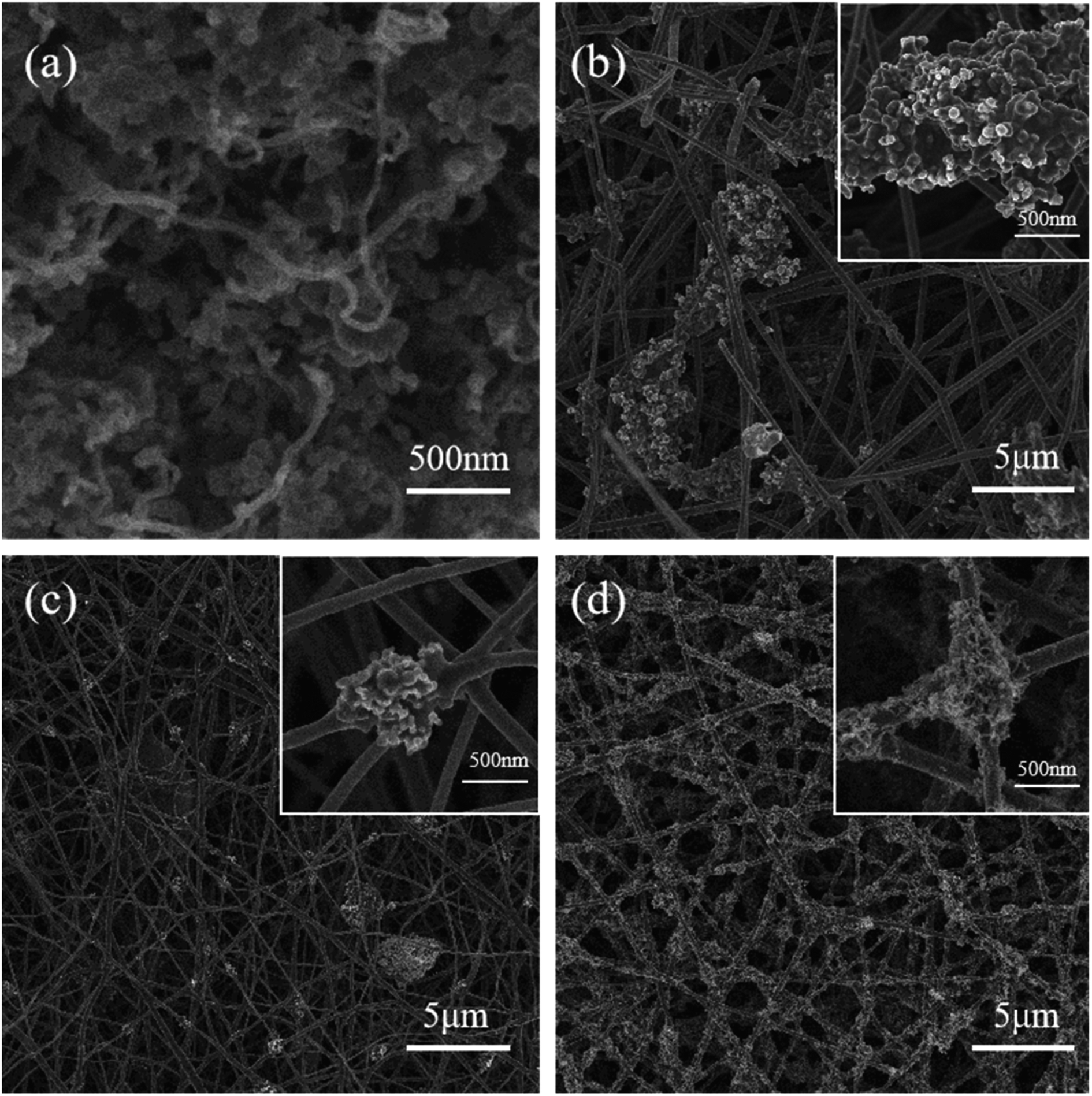 | ||
| Fig. 2 SEM images of (a) Si@CNTs, (b) Si/CNFs, (c) Si@CNTs/CNFs, (d) Si/CNFs/CNTs (the insets are the enlarged SEM images). | ||
Fig. 3a–e show the TEM observations of Si, Si@CNTs, Si/CNFs, Si@CNTs/CNFs, and Si/CNFs/CNTs prepared by electrospinning. The diameter of the raw Si NPs was 60–80 nm. Similar to the SEM images, Si NPs are exposed on the carbon fiber surface and prone to agglomeration during the electrospinning process. Si@CNTs/CNFs exhibits significant particle agglomeration due to the growth of CNTs on the surface of Si NPs. For CNTs, their large surface area and high specific surface area result in increased van der Waals forces between particles, making them prone to agglomeration.29 However, the in situ deposited CNTs grown by CVD on the surface of Si NPs (Fig. 3b) are strongly bonded to Si NPs, and the strong interaction between CNTs causes the Si NPs to approach each other within the carbon fiber as well. In contrast to Si/CNFs and Si@CNTs/CNFs, the issue of agglomeration of Si NPs in Si/CNFs/CNTs has been partially resolved. In situ deposited CNTs grow on the surface of the fibers, and the CNTs grown between Si NPs play a role in isolating them. Moreover, the strong van der Waals forces between the CNTs do not lead to agglomeration of the Si NPs, as the in situ deposited CNTs serve as the decoration of the surface of the CNFs rather than on the surface of the Si NPs. More importantly, the CVD-grown CNTs surround the fibers and are firmly bonded to the substrate, creating a double conductive buffer network with the carbon fibers which can mitigate the bulk expansion of the Si NPs. Therefore, the double conductive buffer network is considered to be beneficial to the electrochemical performance.
 | ||
| Fig. 3 TEM images of (a) Si, (b) Si@CNTs, (c) Si/CNFs, (d) Si@CNTs/CNFs and (e) Si/CNFs/CNTs. (f) HR-TEM image and (g–i) the element mapping images of (e) for Si/CNFs/CNTs. | ||
Fig. 3f further illustrates the structural composition of CNTs generated by in situ CVD. According to the formation mechanism of CNTs, they are formed through a dissolution–diffusion mechanism. In situ CNTs consist of a hollow cavity structure and multiple concentric graphene layers. The diameter of the MWCNTs is approximately 15 nm, and the graphene layers exhibit distinct lattice patterns, indicating crystalline structure rather than amorphous carbon.
The corresponding EDS results of Si/CNFs/CNTs also demonstrate the distribution and types of elements (Fig. 3g–i). The N element in PAN is retained during the heat treatment process, and N-doped CNFs are beneficial for enhancing the conductivity between the fibers and silicon.30 The composite network structure of CNTs and CNFs accelerates the electronic transmission of the electrode and alleviates stress concentration caused by Si NPs, maintaining structural stability during electrode cycling.
The X-ray diffraction (XRD) results of CNFs, Si/CNFs, Si@CNTs/CNTs, and Si/CNFs/CNTs are indicated in Fig. 4a. CNFs without adding Si NPs were prepared with the similar methods and proportions with Si/CNFs for comparison with XRD and Raman results. Pure CNFs exhibit a broad peak in the range of 20°–28°, and this broad peak is also observed in the remaining samples. This broad peak is attributed to the conversion of PAN into amorphous carbon during the carbonization process.31 For Si/CNFs, Si@CNTs/CNTs, and Si/CNFs/CNTs, the diffraction peaks at 28.4°, 47.3°, 56.1°, 69.1°, and 76.3° are indexed to the crystal planes of silicon (1 1 1), (2 2 0), (3 1 1), (4 0 0), and (3 3 1), respectively (JCPDS 27-1402).32 The average crystallite size of Si NPs form XRD pattern were calculated in the range of 60–80 nm. Therefore, the growth of the carbonaceous phase and in situ CNTs do not change the size of Si NPs.The XRD results confirm that the samples consist of both crystalline silicon and amorphous carbon.
 | ||
| Fig. 4 (a) XRD patterns and (b) Raman spectra of CNFs, Si/CNFs, Si@CNTs/CNFs and Si/CNFs/CNTs; (c) FTIR spectra for initial spun fiber, oxidized fiber, carbonized fiber and Si/CNFs/CNTs after CVD; (d) TGA curves pure Si, Si/CNFs, Si@CNTs/CNFs and Si/CNFs/CNTs. | ||
The Raman results of the four samples are indicated in Fig. 4b. The characteristic peaks at approximately 302 cm−1, 515 cm−1, and 952 cm−1 are associated with the vibrational modes of crystalline silicon.33 Additionally, the peaks at around 1350 cm−1 and 1580 cm−1 correspond to the D-band and G-band, respectively. The D-band shows structural defects and amorphous structure of carbon materials, while the G-band represents the ordered crystalline lattice structure of carbon materials. Generally, the ratio of peak intensity R (ID:IG) can be used to characterize the degree of graphitization of the carbon material.34 The R values for CNFs and Si/CNFs are consistent (R = 0.96) proving that the PAN-derived carbon fibers are mainly amorphous carbon. The amorphous structure results in a disordered and non-uniform structure, which may also be attributed to nitrogen doping in amorphous carbon. However, the D-band and G-band peaks in Si@CNTs/CNTs and Si/CNFs/CNTs are not prominent, indicating a high degree of graphitization. Additionally, the R values of Si@CNTs/CNTs and Si/CNFs/CNTs decrease to 0.9 and 0.82, respectively, indicating high-quality and highly conductive CNTs grown by in situ CVD. Consistent with the XRD results, the Raman results show that the Si characteristic peak intensities decrease significantly in Si@CNTs/CNTs and Si/CNFs/CNTs due to the effective deposition of CNTs. Furthermore, the characteristic peak of Si in Si/CNFs/CNTs in Raman spectra shows a small shift towards higher frequencies. This shift may be attributed to the reduction in partial strain within the electrode material, which is beneficial to release stress during volume changes.35
In Fig. 4c, the chemical structures of the initial spun fiber, pre-oxidized fiber, carbonized fiber, and fiber after CVD are characterized by FTIR spectroscopy. The initial spun fiber contains many functional groups because of the PAN precursor. The peaks at 2938 cm−1, 2238 cm−1, and 1728 cm−1 correspond to the –CH2, C![[double bond, length as m-dash]](https://www.rsc.org/images/entities/char_e001.gif) N, and CO bonds in PAN, respectively.36 During the pre-oxidation process, the fiber comes into contact with oxygen, and the carbon atoms on the surface form numerous hydroxyl groups, which corresponds to the increased hydroxyl content at 3600 cm−1 in the FTIR spectrum. After carbonization, non-carbon elements are removed at high temperatures, and the surface functional groups are further reduced, tending to form pure-carbon materials with silicon. The functional groups on the surface of Si/CNFs/CNTs show no significant difference compared to the carbonized sample, indicating that the CNTs by CVD process do not change the overall types of functional groups. It is worth noting that the Si–O–Si bond at 1228 cm−1 is consistently present throughout the material preparation process.37 This is due to the exposure of Si NPs on the fiber surface, which directly contacts oxygen and undergoes slight oxidation to form silicon oxide.
N, and CO bonds in PAN, respectively.36 During the pre-oxidation process, the fiber comes into contact with oxygen, and the carbon atoms on the surface form numerous hydroxyl groups, which corresponds to the increased hydroxyl content at 3600 cm−1 in the FTIR spectrum. After carbonization, non-carbon elements are removed at high temperatures, and the surface functional groups are further reduced, tending to form pure-carbon materials with silicon. The functional groups on the surface of Si/CNFs/CNTs show no significant difference compared to the carbonized sample, indicating that the CNTs by CVD process do not change the overall types of functional groups. It is worth noting that the Si–O–Si bond at 1228 cm−1 is consistently present throughout the material preparation process.37 This is due to the exposure of Si NPs on the fiber surface, which directly contacts oxygen and undergoes slight oxidation to form silicon oxide.
Fig. 4d shows the TGA results of all silicon-based composite materials. At temperatures ranging from room temperature to 200 °C, the weight of the porous materials decreases because residual water is removed. The carbon-based matrix undergoes combustion within the range of 400 °C and 700 °C, and the oxidation of Si NPs occurs above 700 °C, leading to the increased weight. Therefore, the formula for calculating the silicon content in silicon-based composite materials is as follows:
 | (1) |
XPS is used to further elucidate the structural properties and surface conditions of Si/CNFs/CNTs. The XPS measurement of Si/CNFs/CNTs is shown in Fig. 5. The XPS spectra shown in Fig. 5a confirm the presence of O, N, C, and Si elements. There are three peaks in the C 1s spectrum corresponding to C–C bonds (284.8 eV), C–N bonds (286 eV), and CO bonds (288.3 eV).38 Most of the carbon atoms are arranged in the C–C bonds of the conjugated honeycomb lattice. The fitted N 1s spectrum reveals three types of nitrogen doping in Si/CNFs/CNTs, including pyridinic-N, graphitic-N, and oxidized-N.30 This type of nitrogen-doped carbon material can enhance the conductivity of electrode material. The presence of oxidized-N may be attributed to the slight oxidation of carbon fibers during the acid-washing process with dilute nitric acid. Fig. 5d shows the two valence states of silicon, Si0 and Si4+, located around binding energies of 100 eV and 104 eV, respectively.38 The Si4+ state is attributed to the oxidation of Si NPs exposed on the fiber surface, which is also confirmed by the presence of Si–O–Si bonds shown in the FTIR spectrum. However, there is no diffraction peak of silica in the XRD spectrum, indicating that the content of silica is low.13,15,20
 | ||
| Fig. 5 (a) XPS spectrum of Si/CNFs/CNTs, (b) C 1s, (c) N 1s and (d) Si 2p spectra of Si/CNFs/CNTs. | ||
Nitrogen adsorption–desorption isotherms are used to analyze the pore structure of Si/CNFs, Si@CNTs/CNFs, and Si/CNFs/CNTs materials (Fig. 6). Si/CNFs and Si@CNTs/CNFs exhibit typical type I isotherms, while Si/CNFs/CNTs display a typical type IV isotherm, indicating its abundant mesoporous structure on the surface, which is consistent with the pore size distribution obtained from DFT calculations (Fig. 6b).39,40 The abundant mesoporous structure is attributed to the successful deposition of CNTs, as nanoscale CNTs are a common type of mesoporous structure.41 Additionally, Si/CNFs/CNTs composite material exhibits a significant presence of mesopores centered at 3 nm, 7 nm, and 10 nm, as well as abundant micropores centered at around 1.5 nm. Compared to Si/CNFs and Si@CNTs/CNFs, Si/CNFs/CNTs demonstrate a significantly larger specific surface area and total pore volume, as the in situ CNTs are deposited on the surface of carbon fibers rather than within the fibers (Table 1). These mesoporous and microporous structures provide larger void volumes and higher specific surface areas, enhancing the adsorption capacity and increasing the lithium-ion insertion sites, thereby improving the capacity and stability of electrode. Moreover, the high specific surface area of the porous structure can effectively promote electrolyte infiltration and ion conduction, while providing space for buffering and volume expansion of Si NPs, thereby improving the stability of the electrode.
 | ||
| Fig. 6 (a) N2 adsorption–desorption isotherms and (b) pore size distribution of Si/CNFs, Si@CNTs/CNFs and Si/CNFs/CNTs. | ||
| Sample | Specific surface area (m2 g−1) | Average pore size (nm) | Total pore volume (cm3 g−1) |
|---|---|---|---|
| Si/CNFs | 24.58 | 1.68 | 0.04 |
| Si@CNTs/CNFs | 29.43 | 1.76 | 0.05 |
| Si/CNFs/CNTs | 179.6 | 1.41 | 0.26 |
3.2 Electrochemical performance
The cyclic voltammetry (CV) curve of Si/CNFs/CNTs composite material for the first five cycles is shown in Fig. 7a. In the first cycle, a broadened reduction peak appears around 0.83 V, which disappears in subsequent cycles. This is attributed to the formation of solid-electrolyte interphase (SEI) film during the initial charge–discharge process. The sharp peak below 0.1 V and the new typical reduction peak around 0.17 V is related to the alloying process of Li+ with silicon. During the charging process, the oxidation peaks around 0.32 V and 0.51 V represent the delithiation process of LixSi alloy, forming silicon.42 With increasing cycle number, the increase in the area under the CV curve indicates the gradual activation of the Si/CNFs/CNTs composite material.43 | ||
| Fig. 7 (a) CV curves of Si/CNFs/CNTs at first five cycles, (b) charge–discharge curve of Si/CNFs/CNTs at different cycles, (c) cycling performance at 100 mA g−1 and (d) rate performance of Si/CNFs, Si@CNTs/CNFs and Si/CNFs/CNTs. | ||
Fig. 7b illustrates the charge/discharge curves of the Si/CNFs/CNTs composite material for the 1st, 2nd, 10th, 20th, and 50th cycles at a current density of 0.1 C (1 C = 1000 mA g−1). In the first cycle, a continuous descending plateau is observed in the voltage range of 1–0.75 V because of the formation of the SEI film, which corresponds to the broadened reduction peak around 0.83 V in the CV curve. A long plateau appears around 0.1 V in the discharge curve, which is related to the lithiation behavior of crystalline silicon.44 Furthermore, in the first cycle, the discharge capacity of the Si/CNFs/CNTs composite material drops abruptly from 1463.7 mA h g−1 to 914.3 mA h g−1, which is associated with the irreversible loss of Li+ because of Li+ trapped in the amorphous carbon and high specific surface area of CNTs. The large specific surface area of silicon based materials may cause the SEI layer to thicken in the first cycle. In subsequent cycles, plateaus are observed around 0.3 V and 0.51 V, which are related to the delithiation of LixSi alloy, consistent with the results of CV. It is noteworthy that, except for the first cycle, the curves for different cycles almost overlap, demonstrating excellent cycling stability.
Fig. 7c compares the cycling performance of Si/CNFs, Si@CNTs/CNFs, and Si/CNFs/CNTs over the first 100 cycles at a current density of 0.1C. In the first cycle, Si/CNFs exhibit high discharge and charge capacities of 1636.9 mA h g−1 and 1286.6 mA h g−1, respectively. Nevertheless, in the subsequent cycles, Si/CNFs shows significant capacity decay and only delivers a capacity of 110.5 mA h g−1 after 100 cycles with a capacity retention of 8.5%. This is attributed to the direct contact of Si NPs with the electrolyte and the repeated expansion of the Si volume, leading to an unstable SEI film and capacity degradation. The method of encapsulating Si NPs with in situ deposited CNTs has a significant effect on improving the stability of Si@CNTs/CNFs. However, due to the aggregation of silicon and the significant reduction in Si content in the precursor solution, Si@CNTs/CNFs exhibit a more pronounced capacity decrease, reaching 401.2 mA h g−1 after 100 cycles. On the contrary, the Si/CNFs/CNTs composite material, composed of both CNTs and CNFs, does not affect the precursor solution's concentration due to the deposition of CNTs on the fiber surface. Although showing much higher content of Si element compared with Si@CNTs/CNFs, the Si/CNFs/CNTs composite material demonstrates excellent cycling stability during the cycling process, with a capacity retention of 69.9% and a high capacity of 639.9 mA h g−1 maintained after 100 cycles.
To further demonstrate the excellent performance of Si/CNFs/CNTs, the rate capabilities of Si/CNFs, Si@CNTs/CNFs, and Si/CNFs/CNTs were measured at different current densities (Fig. 7d). Si/CNFs/CNTs exhibits discharge-specific capacities of 880.3 mA h g−1, 775.2 mA h g−1 and 660.4 mA h g−1 at current densities of 0.1 C, 0.2 C and 0.5 C, respectively. At higher current densities of 1 C, 2 C and 5 C, the specific capacities of Si/CNFs/CNTs decrease to 520.9 mA h g−1, 410.6 mA h g−1 and 160.3 mA h g−1, respectively, demonstrating excellent rate performance. Moreover, when the current density returned to 0.1 C, Si/CNFs/CNTs exhibits a high specific capacity of 796 mA h g−1, and it maintains excellent cycling stability over the next 40 cycles. In comparison, Si/CNFs and Si@CNTs/CNFs show significantly lower rate capabilities than the Si/CNFs/CNTs composite material. Si/CNFs exhibits a higher discharge capacity of 1000.6 mA h g−1 due to its higher Si content when the current density returns to 0.1 C, surpassing the specific capacity of Si/CNFs/CNTs. However, its capacity sharply decreases over the next 40 cycles and approaches the specific capacity of Si/CNFs/CNTs after 100 cycles. Si@CNTs/CNFs, on the other hand, shows good stability when the current density returned to 0.1 C but has a lower discharge capacity of only 621.7 mA h g−1. These results indicate that the dual-conductive buffering network of CNTs and CNFs in Si/CNFs/CNTs can effectively protect Si NPs, facilitate Li+ transport, and maintain the stability of the electrode structure.
Si/CNFs/CNTs composite material exhibits excellent lithium-storage capacity, which is related to pseudocapacitance. Pseudocapacitance can be used to evaluate the interface characteristics between the electrolyte and the electrode. CV curves in the scanning range of 0.2–1.0 mV s−1 were studied in Fig. 8a. The CV curves at different scan rates show slight shifts and exhibit two peaks, suggesting that electrode polarization is slight.38 The storage of Li+ involves two mechanisms: diffusion-controlled charge storage and capacitive charge storage. The functional relationship between current (i) and scan rate (v) is given by the following equations (formulas (2) and (3)).45
| i = av | (2) |
|
log(i) = blog(v) + log(a)
| (3) |
 | ||
| Fig. 8 (a) CV curves of the Si/CNFs/CNTs electrode at various scan rates from 0.2–1.0 mV s−1; (b) log(i)/log(v) plots of Si/CNFs/CNTs the electrode at various scan rates from 0.2 to 1.0 mV s−1; (c) capacitive contribution at 1.0 mV s−1; (d) the percentages of capacitive contributions at various scan rate; (e) Nyquist plots of Si/CNFs, Si@CNTs/CNFs and Si/CNFs/CNTs; (f) Nyquist plots of Si/CNFs/CNTs before and after 20 cycles. | ||
The calculated value of parameter b reflects the lithium storage mechanism of the composite material. When b approaches 0.5, the electrode is primarily governed by a diffusion-controlled charge storage mechanism, while b tending to 1 indicates that the electrode is primarily governed by the surface capacitance (pseudocapacitance) storage mechanism.46 As shown in Fig. 8b, during the charging/discharging process, there are two main peaks the values of b are between 0.5 and 1.0, indicating that the electrochemical process of Si/CNFs/CNTs composite material is simultaneously influenced by diffusion behavior and pseudocapacitance behavior, with a relatively balanced contribution from both mechanisms. To further quantify the contribution of pseudocapacitive charge to the capacity, the following formula can be used to calculate the capacity contribution rate.
| i(V) = k1v + k2v1/2 | (4) |
To further evaluate the electronic conductivity of the composite material, Electrochemical Impedance Spectroscopy (EIS) testing and equivalent circuits were employed. Fig. 8e shows the Nyquist plots of Si/CNFs, Si@CNTs/CNFs, and Si/CNFs/CNTs before cycling, along with their corresponding equivalent circuit simulation models. Rs represents the Ohmic resistance of the electrode, observed as the intercept with the X-axis in the Nyquist plot. Rct represents the charge transfer impedance. The slanted line in the low-frequency region represents the Warburg diffusion impedance Zw, representing the diffusion impedance within the electrode material.49 Table 2 presents the values of Rs, Rct, and Zw for the three samples. The Rs values of the batteries are similar and relatively small. Si/CNFs/CNTs exhibit significantly reduced charge transfer impedance (Rct) of only 60.1 Ω, while Si/CNFs and Si@CNTs/CNFs have Rct values of 119.6 Ω and 102.1 Ω, respectively. A low Rct value indicates a high charge transfer rate in the electrode and efficient transport within the battery, attributed to the deposition of CNTs on the fiber surface. Fig. 8f depicts the Nyquist plot of Si/CNFs/CNTs self-supported anode before and after 20 cycles to confirm its stable electrochemical performance. The Rct value significantly decreases from 60.1 Ω to 6.4 Ω after cycling, indicating the surface stability of the composite material during battery cycling with improved kinetics.50
| Sample | Rs (Ω) | Rct (Ω) | Zw (Ω) |
|---|---|---|---|
| Si/CNFs | 3.58 | 119.6 | 103.2 |
| Si@CNTs/CNFs | 3.91 | 102.1 | 28.4 |
| Si/CNFs/CNTs | 2.91 | 60.1 | 14.5 |
Table 3 synthesized some electrochemical properties of self-supported silicon-based anodes. For example, Kim et al. formed G/Si by combining negatively charged GO with positively charged silicon and used electrostatic spinning to confine it in carbon fibers to form GSP. GSP still has a capacity of 600 mA h g−1 after 100 cycles at a current density of 100 mA g−1. Overall, compared to other materials, Si/CNFs/CNTs have relatively high specific capacity and stability due to the unique way in which CNTs exist.
In addition, the surface morphology of Si/CNFs, Si@CNTs/CNFs, and Si/CNFs/CNTs by SEM after charge–discharge cycles were provided to further investigate the structural stability of the composite material. As shown in Fig. 9, significant cracks are observed on the surfaces of Si/CNFs and Si@CNTs/CNFs after 100 cycles, which can be attributed to the volume changes resulting from the direct contact between exposed Si and the electrolyte. This was demonstrated by TEM images where ruptured SEI layers were observed. In contrast, the surface of the Si/CNFs/CNTs composite electrode remains smooth without noticeable cracks even after 100 cycles, which can be attributed to its good conductivity and low volume expansion. Also, stable and continue SEI layer was observed in Fig. 9i. This conclusion is further supported by the Nyquist plots before and after cycling, demonstrating the excellent structural stability of the Si/CNFs/CNTs composite electrode. It is worth mentioning that the Si/CNFs/CNTs electrode material after 100 cycles exhibits more complete impregnation by the electrolyte and a smoother surface compared to Si/CNFs. Si/CNFs usually have poor electrolyte wettability, which is a challenge in this system.4 However, the in situ deposited CNTs with no hydroxyl functional groups that can interact with the electrolyte provide high conductivity and surface area. Due to the high conductivity of in situ CNTs, the electrons can be quickly distributed throughout the structure, facilitating the uniform distribution of ions from the electrolyte on the surface of Si/CNFs/CNTs electrode material. Additionally, the large surface area facilitates the diffusion and adsorption of electrolyte molecules, thereby improving the wettability of the electrolyte on the electrode material's surface.
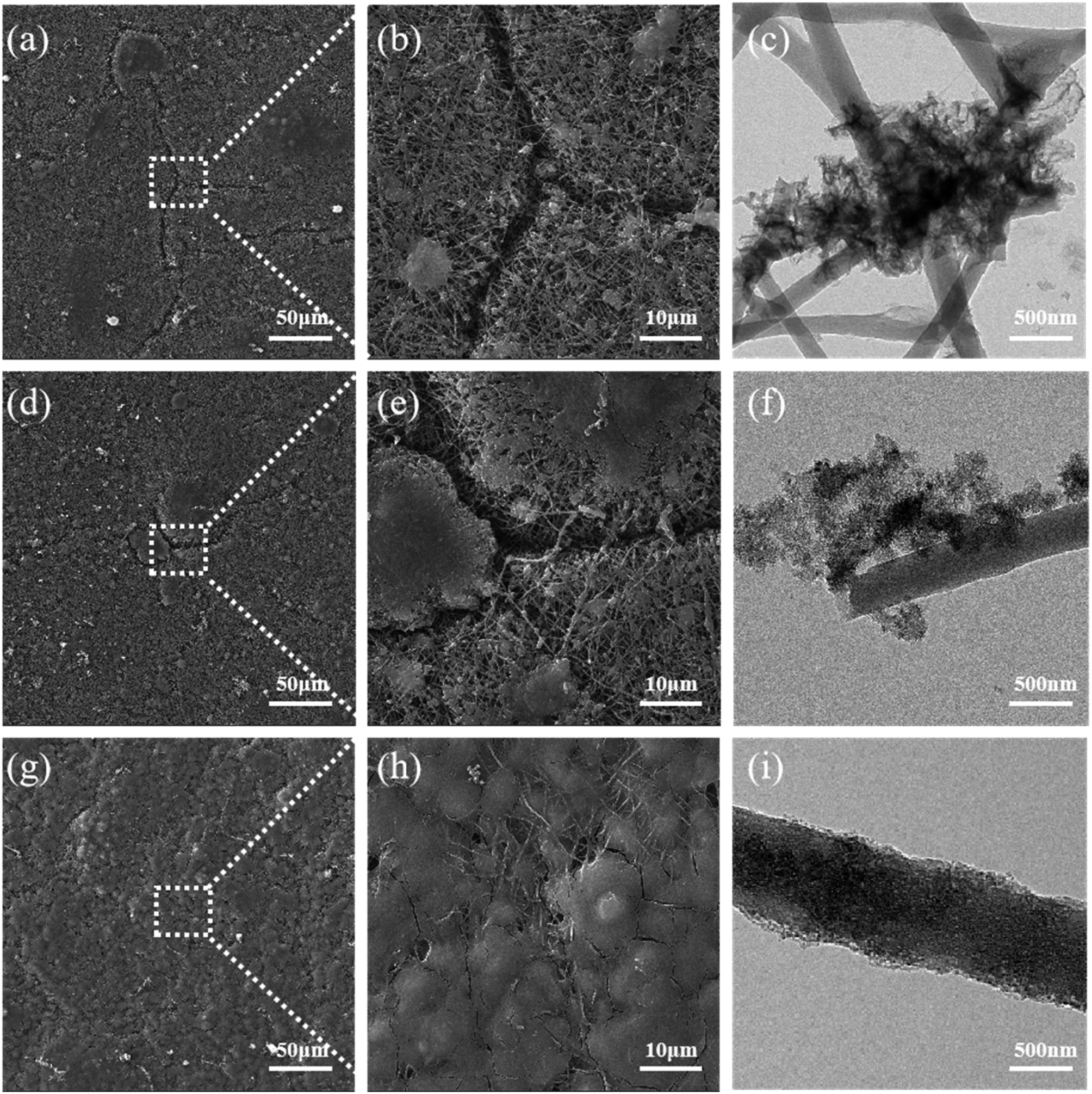 | ||
| Fig. 9 (a–c) SEM and TEM images of Si/CNFs after 100 cycles; (d–f) SEM and images of Si @CNTs/CNFs after 100 cycles; (g–i) SEM and TEM images of Si/CNFs/CNTs after 100 cycles. | ||
Based on the above discussion, the outstanding electrochemical performance of the Si/CNFs/CNTs free-standing anode can be attributed to the synergistic effect of CNTs and CNFs in forming a dual-conductive buffering network. Specifically, electrospinning technology enables the highly uniform dispersion of catalyst particles within the fibers, while the in situ deposition of CNTs brings high conductivity and toughness, serving as a buffer to alleviate the volumetric expansion of Si NPs. The in situ CNTs, firmly combined with the substrate form an interdependent network structure with CNFs, which facilitates the overall improvement of electrochemical performance.
4 Conclusion
In conclusion, we prepared a novel anode (Si/CNFs/CNTs) with a dual-conductive network of CNFs and CNTs by combining electrospinning and in situ chemical vapor deposition without any conductive additives or binders. The in situ deposited CNTs were grown on the surface of CNFs through in situ chemical vapor deposition, forming an elastic buffering layer on the CNFs and Si NPs surfaces to mitigate the concentrated stress caused by the volumetric expansion of Si NPs. The flexible CNTs, with their excellent conductivity and low cost, facilitated electron transfer and reduced the cycling impedance of LIBs. Moreover, the in situ deposited CNTs with a large surface area accelerated the diffusion and adsorption of the electrolyte on the electrode surface. The N-doped CNFs in the composite material accelerate electron transport. Above all, the synergistic effect of CNTs and CNFs leads to the impressive stability of Si/CNFs/CNTs. The Si/CNFs/CNTs electrode material exhibits a high discharge capacity of 639.9 mA h g−1 and a capacity retention of 69.9% at a current density of 100 mA g−1. Considering the excellent performance of Si/CNFs/CNTs, as well as the useful structure and low cost of CNTs, the reported Si/CNFs/CNTs electrode will have great commercial potential for next-generation Li-ion batteries.Author contributions
Yixin Zhao: writing – original draft, validation, investigation. Xingchen Pan: writing – review & editing, investigation, resources. Mingqi Liu: writing – review & editing, methodology, formal analysis. Xiangxiang Chen: writing – review & editing. Rui Zhang: writing – review & editing. Zhiyong Xie: supervision, funding acquisition.Conflicts of interest
There are no conflicts to declare.Acknowledgements
This research was funded by the National Key Research and Development Program of China, grant number 2020YFB1505904 and 2020YFB1505901.References
- W. Wang, Y. Feng, S. Zhang, M. Wang, W. Song, L. Yue, M. Ge and J. Mi, J. Alloys Compd., 2022, 905, 164247 CrossRef CAS.
- K. Xie, J. Wang, S. Yu, P. Wang and C. Sun, Arabian J. Chem., 2021, 14, 103161 CrossRef CAS.
- M. Yang, W. Zhang, D. Su, J. Wen, L. Liu and X. Wang, J. Colloid Interface Sci., 2022, 605, 231–240 CrossRef CAS PubMed.
- X. Zhao, N. Kalidas and V.-P. Lehto, J. Power Sources, 2022, 529, 231269 CrossRef CAS.
- X. Min, G. Xu, B. Xie, P. Guan, M. Sun and G. Cui, Energy Storage Mater., 2022, 47, 297–318 CrossRef.
- W. M. Dose, S. Kim, Q. Liu, S. E. Trask, A. R. Dunlop, Y. Ren, Z. Zhang, T. T. Fister and C. S. Johnson, J. Mater. Chem. A, 2021, 9, 12818–12829 RSC.
- J.-Y. Li, G. Li, J. Zhang, Y.-X. Yin, F.-S. Yue, Q. Xu and Y.-G. Guo, ACS Appl. Mater. Interfaces, 2019, 11, 4057–4064 CrossRef CAS PubMed.
- X. Huang, R. Guo, Y. Lin, Y. Cao and J. Wu, Electrochim. Acta, 2022, 422, 140546 CrossRef CAS.
- H. Tao, L.-Z. Fan, W.-L. Song, M. Wu, X. He and X. Qu, Nanoscale, 2014, 6, 3138–3142 RSC.
- L. Wang, Z. Liu, Q. Guo, X. Guo and J. Gu, RSC Adv., 2017, 7, 36735–36743 RSC.
- S. Liu, W. Xu, C. Ding, J. Yu, D. Fang, Y. Ding and H. Hou, Appl. Surf. Sci., 2019, 494, 94–100 CrossRef CAS.
- Y. Wang, X. Wen, J. Chen and S. Wang, J. Power Sources, 2015, 281, 285–292 CrossRef CAS.
- W. Li, J. Peng, H. Li, Z. Wu, Y. Huang, B. Chang, X. Guo, G. Chen and X. Wang, ACS Appl. Energy Mater., 2021, 4, 8529–8537 CrossRef CAS.
- M. Cao, F. Liao, Q. Wang, W. Luo, Y. Ma, X. Zheng, Y. Wang and L. Zhang, J. Alloys Compd., 2021, 859, 157867 CrossRef CAS.
- X. Li, X. Wang, J. Li, G. Liu, D. Jia, Z. Ma, L. Zhang, Z. Peng and X. Zhu, Electrochem. Commun., 2022, 137, 107257 CrossRef CAS.
- Z. Li, Y. Zhang, T. Liu, X. Gao, S. Li, M. Ling, C. Liang, J. Zheng and Z. Lin, Adv. Energy Mater., 2020, 10, 1903110 CrossRef CAS.
- T. T. Yu, H. L. Liu, M. Huang, J. H. Zhang, D. Q. Su, Z. H. Tang, J. F. Xie, Y. J. Liu, A. H. Yuan and Q. H. Kong, RSC Adv., 2017, 7, 51807–51813 RSC.
- Z. Zhang, H. Ying, P. Huang, S. Zhang, Z. Zhang, T. Yang and W.-Q. Han, Chem. Eng. J., 2023, 451, 138785 CrossRef CAS.
- Y. Li, G. Xu, L. Xue, S. Zhang, Y. Yao, Y. Lu, O. Toprakci and X. Zhang, J. Electrochem. Soc., 2013, 160, A528–A534 CrossRef CAS.
- M. Gao, Z. Tang, M. Wu, J. Chen, Y. Xue, X. Guo, Y. Liu, Q. Kong and J. Zhang, J. Alloys Compd., 2021, 857, 157554 CrossRef CAS.
- M. Dirican, O. Yildiz, Y. Lu, X. Fang, H. Jiang, H. Kizil and X. Zhang, Electrochim. Acta, 2015, 169, 52–60 CrossRef CAS.
- S. Liang, X. Pei, W. Jiang, Z. Xu, W. Wang, K. Teng, C. Wang, H. Fu and X. Zhang, Electrochim. Acta, 2019, 322, 134696 CrossRef CAS.
- Y. Park, M. Oh, J. S. Park, S.-H. Baek, M. Kim, S. Kim and J. H. Kim, Carbon, 2015, 94, 9–17 CrossRef CAS.
- B. Joshi, E. Samuel, Y. I. Kim, M.-W. Kim, H. S. Jo, M. T. Swihart, W. Y. Yoon and S. S. Yoon, Chem. Eng. J., 2018, 351, 127–134 CrossRef CAS.
- Y. Jin, Z. Ai, Y. Song, X. Zhang, J. Shi and C. Ma, Mater. Res. Bull., 2023, 167, 112429 CrossRef CAS.
- W. Li, Z. Xie, S. Qiu, H. Zeng, M. Liu and G. Wu, Nanomaterials, 2023, 13, 365 CrossRef CAS PubMed.
- Z.-D. Yang, X.-Y. Yang, T. Liu, Z.-W. Chang, Y.-B. Yin, X.-B. Zhang, J.-M. Yan and Q. Jiang, Small, 2018, 14, 1800590 CrossRef PubMed.
- J. Pan, L. Bian, H. Zhao and Y. Zhao, Comput. Mater. Sci., 2016, 113, 21–26 CrossRef CAS.
- Y. Wang, F. Wei, G. S. Gu and H. Yu, Phys. B, 2002, 323, 327–329 CrossRef CAS.
- S.-J. Kim, M.-C. Kim, S.-B. Han, G.-H. Lee, H.-S. Choe, D.-H. Kwak, S.-Y. Choi, B.-G. Son, M.-S. Shin and K.-W. Park, Nano Energy, 2016, 27, 545–553 CrossRef CAS.
- S.-H. Park, H.-G. Lee, J.-H. Ju, S.-H. Park, G.-B. Cho and K.-W. Kim, J. Nanosci. Nanotechnol., 2020, 20, 7039–7044 CrossRef CAS PubMed.
- X. Ma, G. Hou, Q. Ai, L. Zhang, P. Si, J. Feng and L. Ci, Sci. Rep., 2017, 7, 9642 CrossRef PubMed.
- Y. Xu, T. Yuan, Z. Bian, H. Sun, Y. Pang, C. Peng, J. Yang and S. Zheng, Compos. Commun., 2019, 11, 1–5 CrossRef.
- Y. Ren, L. Xiang, X. Yin, R. Xiao, P. Zuo, Y. Gao, G. Yin and C. Du, Adv. Funct. Mater., 2022, 32, 2110046 CrossRef CAS.
- J. Yang, Y. Wang, W. Li, L. Wang, Y. Fan, W. Jiang, W. Luo, Y. Wang, B. Kong, C. Selomulya, H. K. Liu, S. X. Dou and D. Zhao, Adv. Mater., 2017, 29, 1700523 CrossRef PubMed.
- J. Yu, C. Zhang, W. Wu, Y. Cai and Y. Zhang, Appl. Surf. Sci., 2021, 548, 148944 CrossRef CAS.
- X. Lu, P. Xu, W. Song, P. Zhou, M. Liao, G. Zeng, X. Hu, J. Li, M. Zhang, Q. Huang and Z. Su, J. Alloys Compd., 2023, 938, 168646 CrossRef CAS.
- X. Xu, F. Wu, W. Yang, X. Dai, T. Wang, J. Zhou, J. Wang and D. Guo, ACS Sustainable Chem. Eng., 2021, 9, 13215–13224 CrossRef CAS.
- Y. Gao, X. Qiu, X. Wang, A. Gu, X. Chen and Z. Yu, Mater. Today Commun., 2020, 25, 101589 CrossRef CAS.
- X. Zhuang, Y. Zhang, L. He, Y. Zhu, Q. Tian, X. Guo, J. Chen, L. Li, Q. Wang, G. Song and X. Yan, Electrochim. Acta, 2017, 249, 166–172 CrossRef CAS.
- F. Gao, C. Geng, N. Xiao, J. Qu and J. Qiu, Carbon, 2018, 139, 1085–1092 CrossRef CAS.
- H.-J. Shin, J.-Y. Hwang, H. J. Kwon, W.-J. Kwak, S.-O. Kim, H.-S. Kim and H.-G. Jung, ACS Sustainable Chem. Eng., 2020, 8, 14150–14158 CrossRef CAS.
- Q. Yun, X. Qin, Y.-B. He, W. Lv, Y. V. Kaneti, B. Li, Q.-H. Yang and F. Kang, Electrochim. Acta, 2016, 211, 982–988 CrossRef CAS.
- N. Liu, H. Wu, M. T. McDowell, Y. Yao, C. Wang and Y. Cui, Nano Lett., 2012, 12, 3315–3321 CrossRef CAS PubMed.
- Y. Zhang, G. Zhao, P. Ge, T. Wu, L. Li, P. Cai, C. Liu, G. Zou, H. Hou and X. Ji, Inorg. Chem., 2019, 58, 6410–6421 CrossRef CAS PubMed.
- S. Tao, Z. Luo, R. Momen, K. Zou, B. Wang, X. Deng, X. Xiao, W. Deng, Y. Liu, H. Hou, G. Zou and X. Ji, Chem. Eng. J., 2022, 446, 137070 CrossRef CAS.
- Y. Zhang, C. Liu, X. Gao, Z. Luo, J. Hu, G. Zou, H. Hou, Z. Xu and X. Ji, Nano Energy, 2020, 68, 104333 CrossRef CAS.
- P. Zhou, S. Qi, M. Zhang, L. Wang, Q. Huang, Z. Su, Z. Guo, Y. Hu, Y. Wang and S. Chen, Electrochim. Acta, 2021, 367, 137449 CrossRef CAS.
- Z. Song, G. Zhang, X. Deng, Y. Tian, X. Xiao, W. Deng, H. Hou, G. Zou and X. Ji, Adv. Funct. Mater., 2022, 32, 2205453 CrossRef CAS.
- Z. Yi, N. Lin, Y. Zhao, W. Wang, Y. Qian, Y. Zhu and Y. Qian, Energy Storage Mater., 2019, 17, 93–100 CrossRef.
- Y. Li, G. Xu, Y. Yao, L. Xue, M. Yanilmaz, H. Lee and X. Zhang, Solid State Ionics, 2014, 258, 67–73 CrossRef CAS.
- S. Y. Kim, K. S. Yang and B.-H. Kim, J. Power Sources, 2015, 273, 404–412 CrossRef CAS.
- Q. Liu, Y. Gao, P. He, C. Yan, Y. Gao, J. Gao, H. Lu and Z. Yang, Mater. Lett., 2018, 231, 205–208 CrossRef CAS.
| This journal is © The Royal Society of Chemistry 2023 |