
 Open Access Article
 This Open Access Article is licensed under a Creative Commons Attribution-Non Commercial 3.0 Unported Licence
Interference micro/nanolenses of salts for local modulation of Raman scattering†
Yun-Tae Kima,
Cheongha Leea,
Seongyeop Lima and
Chang Young Lee *ab
*ab
aSchool of Energy and Chemical Engineering, Ulsan National Institute of Science and Technology (UNIST), Ulsan 44919, Republic of Korea. E-mail: cylee@unist.ac.kr
bGraduate School of Carbon Neutrality, Ulsan National Institute of Science and Technology (UNIST), Ulsan 44919, Republic of Korea
First published on 3rd November 2023
Abstract
Micro/nanolenses play a crucial role in optics and spectroscopy, but the effect of interference patterns within each lens has been largely unexplored. Herein, we investigate modulation of Raman scattering by the interference within a single micro/nanolens of a hygroscopic salt. Lenses having two different diameter (d) ranges, d > 2 μm and d ∼1 μm, are placed on a silicon substrate, followed by collection of a Raman intensity map of the silicon peak. Lenses with d > 2 μm show dark and bright circular fringes in the Raman map, resembling the Newton's rings formed by optical interference. In the smaller lenses (d ∼1 μm), the map yields only a single peak at the center, representing either an intensity maximum or minimum. In both diameter ranges, whether the Raman intensity is enhanced or suppressed is determined by interference conditions, such as wavelength of the excitation laser or thickness of the SiO2 layer. The interference in salt micro/nanolenses finds applications in local modulation of Raman scattering of a nanoscale object, as demonstrated in individual single-walled carbon nanotubes decorated with the salt lenses.
Introduction
Interference of reflected light at material interfaces has been widely used in optics and spectroscopy of nanomaterials, such as optical visualization1,2 and interference-enhanced Raman scattering (IERS)3–7 of graphene. In micro/nanolenses having a plano-convex shape, interference causes formation of concentric and alternating patterns of dark and bright fringes, called Newton rings as reported in polymeric micro/nanolenses,8–10 water or oil droplets,11–13 and graphene bubbles.14,15 The interference patterns within a micro/nanolens can find potential applications in nanomaterials research, by locally modulating optical or spectral properties of a nanoscale specimen underneath the lens. Since Raman spectroscopy has served as a powerful tool for characterizing low-dimensional nanomaterials,16 the interference in those lenses will be particularly useful in Raman spectroscopy. While previous studies demonstrated overall modulation of Raman scattering by interference,3–7 it is largely unknown how the interference within a micro/nanolens causes local modulation of Raman scattering of the underlying specimen. Moreover, the effect of interference in micro/nanolenses has been overlooked compared to that of the size,17 shape,18–21 and refractive indices22 of the lenses. Hence, understanding the interference in such lenses may offer new opportunities, for example, in sub-diffraction-limit microscopy,17,18,20,23 light harvesting in solar cells,24 and spectral amplification.25–27In this work, we demonstrate that the optical interference in salt micro/nanolenses strongly modulates the local intensity of Raman scattering of a specimen underneath the lens. Upon decreasing the size of the salt lens, the number of Newton rings decreases, ultimately forming only a single ring in nanoscale salt lenses. Such lenses serve as a unique tool for the enhancement or suppression of Raman scattering of the underlying specimen, as confirmed with silicon substrates at various interference conditions: oxide thickness, lens diameter, and wavelength of excitation laser. As an application of the interference micro/nanolenses of salts, we show formation of salt lenses selectively along a single-walled carbon nanotube (SWNT), via transport of ions along the exterior of the material, and demonstrate local modulation of Raman scattering of the nanotube. This work not only provides understanding of the interference micro/nanolenses in Raman spectroscopy but suggests broad applications of the lenses in nanomaterials research.
Results and discussion
The hygroscopicity of alkali metal halides can be utilized to create liquid-state micro/nanolenses. The phase of such lenses is determined by deliquescence relative humidity (DRH) above which the salt becomes aqueous solution by absorbing moisture from the air, as well as efflorescence relative humidity (ERH) below which the solution dries back to salt crystals by evaporation of water.28 We formed hygroscopic salt lenses on silicon substrates having various oxide thicknesses using a simple air-spray method. When the lens was sprayed on a silicon substrate with an oxide layer, as illustrated in Fig. 1a, the reflection and refraction of light occurred at the interfaces of air/lens and lens/substrate, forming constructive or destructive interference patterns known as Newton rings. Fig. 1b shows top-view optical image of a LiCl microlens on 300 nm SiO2/Si substrate under ambient condition (25.0 °C, 54% relative humidity). The image clearly shows Newton rings.8 Here, the LiCl microlens is an aqueous droplet, which maintains its liquid state under a broad range of ambient conditions because of the low DRH of LiCl (11.3%). Fig. 1c shows a false-colored and side-view environmental SEM image of an aqueous NaCl lens above DRH of NaCl (75%), having the diameter (d) of 1.3 μm, the height of 0.23 μm, and the contact angle of 37°. The contact angle of the aqueous lens on a silicon substrate with 300 nm SiO2 remained invariable at 37 ± 4° over the diameter range of 1–11 μm (Fig. 1d), as similarly reported in the previous studies of aqueous microlenses on SiO2 substrate.29,30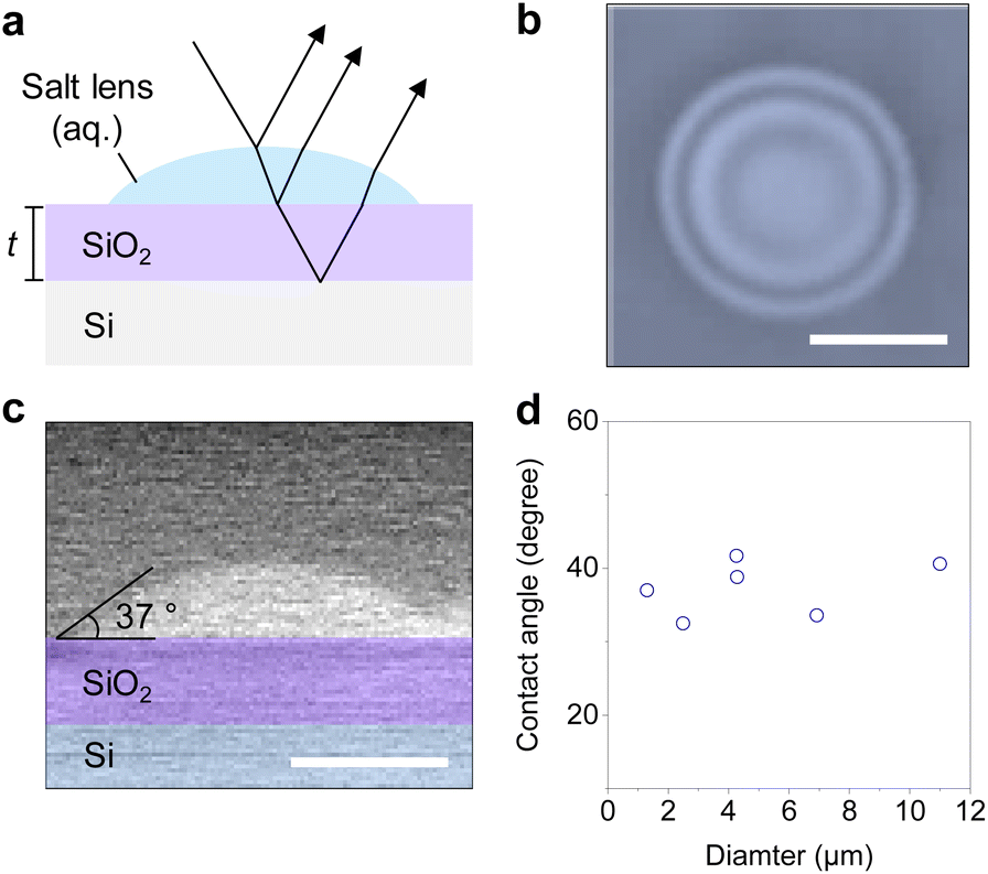 | ||
| Fig. 1 Interference phenomenon in salt microlenses. (a) Schematic illustration showing interference phenomenon in salt microlens on SiO2/Si substrate. (b) Top-view optical image of LiCl (aq.) microlens on SiO2/Si substrate, showing the Newton rings formed by light interference. Scale bar: 3 μm. (c) Side-view environmental SEM image of NaCl (aq.) microlens on SiO2/Si substrate at 100% RH (>DRH). SiO2/Si layers are false colored for better contrast. Scale bar: 500 nm. (d) Contact angles measured from various diameters of salt microlenses on SiO2/Si substrate. | ||
The Raman intensity modulated by the LiCl microlens is strongly correlated with the Newton rings. As shown in Fig. 2a, we placed a LiCl lens (d = 6 μm) on a 300 nm SiO2/Si substrate and obtained an optical contrast map (top left) and a Raman intensity map of silicon peak (520 cm−1) at 532 nm excitation (bottom left), with the corresponding intensity profiles along the dotted line in each map plotted on the right. The optical map showed three Newton rings, whereas the number decreased to two in the Raman map. Repeating the measurements on a 150 nm SiO2/Si substrate, using another LiCl lens (d = 4 μm), gave a similar trend, with the number of Newton rings decreased and the phases inverted in the Raman map (Fig. 2b). It is worth noting that the thinner oxide enhances the Raman intensity at the center of the lens, suggesting a significant role of interference in the system. The intensity profiles of the optical and Raman maps illustrate that the phases of the fringes in the two maps are generally inverted. However, this phase inversion is not entirely opposite, presumably due to the contrasting properties of the incident lights: white light with uniform intensity; versus laser light with a Gaussian intensity profile. While our study prioritizes experimental investigations, complementary approaches such as finite-difference time-domain (FDTD) simulations, or image processing,10 could offer a deeper understanding of the correlation between the optical and Raman maps.
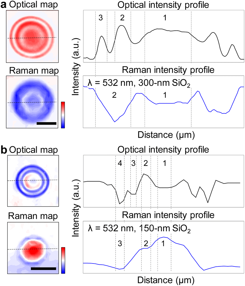 | ||
| Fig. 2 Relationship between Raman intensity of microlens and optical interference. Top-view false-color optical image of LiCl microlenses (top) and Raman intensity map of Si peak at 520 cm−1 from the lenses (bottom) on silicon substrates with (a) 300 nm SiO2 and (b) 150 nm SiO2. Shown on the right are intensity profiles along the dotted lines. Scale bars: 3 μm. | ||
We considered various experimental parameters potentially affecting the Raman scattering. The phases of the circular fringe patterns and the locations of the maximum intensity varied with the thickness of the oxide layer, excitation wavelength, and diameter of lenses (Fig. S1†). The phase of the circular rings in the Raman map did not depend on the focal plane of the excitation laser (Fig. S2†). Further, the shape of the liquid-state lens before and after laser irradiation remained almost the same (Fig. S3†). In all the silicon substrates used in this study, the root-mean-square roughness remained insignificant compared with the lens diameter: 0.08 nm on bare Si, 0.12 nm on 150 nm SiO2/Si, and 0.26 nm on 300 nm SiO2/Si (Fig. S4†). The constant contact angle of the lens (Fig. 1d) suggests that the curvature effect is insignificant. Thus, under our experimental conditions we rule out the effects of focal plane of the laser, change of the lens shape or curvature, and surface roughness of the substrate on the light transmission through the lens. We therefore conclude that the two different Raman scattering patterns in Fig. 2 result solely from the interference effects.
Modulation of Raman scattering by the lens was further investigated under various interference conditions. Fig. 3a shows the number of Newton rings in LiCl microlenses plotted versus lens diameter at difference oxide thicknesses of the silicon substrate. Here each data point was obtained from a single lens. The number of rings in optical images decreased as the diameter of lens decreased as reported previously.8 In the Raman intensity maps of a silicon peak (520 cm−1), the number of rings also decreased in the smaller lenses, forming only a single peak in the intensity profile when d ∼1 μm (Fig. 3b). At 633 nm excitation, the peak was an intensity maximum on a bare silicon or a silicon with 300 nm oxides, and an intensity minimum on a silicon with 150 nm oxides. At 532 nm excitation, the intensity profiles were reversed in the two oxides: a maximum in the 150 nm SiO2 and a minimum in the 300 nm SiO2 (Fig. 3c). The results confirm the interference-dependent Raman scattering of specimen underneath the lenses since the absorbance for the salt solution does not change in the visible wavelength range (Fig. S5†).
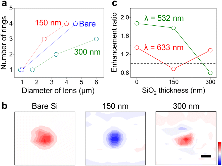 | ||
| Fig. 3 Characterization of interference micro/nanolenses. (a) Number of Newton rings in optical images plotted versus lens diameter at different oxide thicknesses. (b) Raman intensity maps of silicon (520 cm−1) at 633 nm excitation, modulated by a LiCl lens (d ∼1 μm) placed on silicon substrate with various oxide thicknesses. Only a single ring appears in the optical image and Raman map. Scale bar: 1 μm. (c) Raman enhancement by the lens on silicon substrate with different oxide thicknesses at 532 nm (green) and 633 nm (red) excitation. The dotted line indicates the enhancement ratio of 1. | ||
The interference lens based on hygroscopic salts, when placed on a nanoscale specimen, can be used for locally modulating Raman scattering of the specimen, which we demonstrate using single-walled carbon nanotubes (SWNTs). Raman spectroscopy is an important tool for the study of carbon nanomaterials such as graphene and carbon nanotubes. In graphene, owing to its single-atom-thickness, much of the incident light is transmitted and only 2.3% of it is used for Raman scattering in the visible range.31,32 As a result, the Raman signal of graphene is very weak. Thus, multiple light reflections based on interference phenomena have been widely used for the enhancement of Raman scattering.3–6,33–36 For carbon nanotubes, however, the magnitude of the Raman signal is governed by strong resonance-Raman scattering conditions. Therefore, the interference effect in the Raman scattering of carbon nanotubes has been somewhat overlooked although recent studies29,30 of hygroscopic salt lenses suggest crucial role of interference.
Compared to existing solid- or liquid-state lenses, salt lenses offer several advantages as unique tools for nanomaterials research. First, salt lenses can be selectively formed along 1D nanomaterials by transporting an ionic solution through the material, a feat challenging for most solid-state micro/nanolenses. Secondly, salt lenses can be readily removed by rinsing with water, without damaging or altering the properties of the nanomaterials. Lastly, when hygroscopic salts are used above their DRH, these lenses transform into aqueous droplets of the corresponding ionic solution. These micro/nano droplets, with their high surface-to-volume ratio, can capture gaseous molecules from the environment, enabling Raman analysis of those molecules.30 Several liquid-state micro/nanodroplets share some of the aforementioned advantages. Examples include the formation of ionic liquid37 or PMMA38 droplets along a nanowire by molecular transport, as well as the controlled formation of oil nanodroplets12,13 for various applications including Raman spectroscopy. However, none have demonstrated aqueous micro/nanodroplets for use in Raman spectroscopy.
In this study, we decorated carbon nanotubes with NaCl lenses by utilizing exterior transport along the nanotubes, as reported previously29,39 and verified by the SEM image (Fig. S6†). Fig. 4a shows an optical micrograph of a SWNT decorated with NaCl lenses on a 300 nm SiO2/Si substrate (top) and the corresponding Raman map of the G-band of the nanotube (bottom) at excitation wavelengths of 532 nm and 633 nm. Shown on the right are the Raman spectra collected from the red spot in the optical micrograph with (blue) or without (black) the lens at each wavelength. Note that only a small portion of a centimeter-long SWNT was characterized in the figure. Here the lens shape and the location of the nanotube under the lens did not affect the Raman spectra because the spectra were obtained from the same lenses. The results clearly demonstrate that the Raman scattering of the nanotube beneath the lens strongly depends on the excitation wavelength, showing enhancement at 633 nm and suppression at 532 nm. The small lens diameter, as described in Fig. 3, prevented the observation of the circular fringe patterns within each lens. For the bare silicon substrate, however, the Raman scattering of the nanotube was enhanced by the lens at both excitation wavelengths (Fig. 4b). Although the enhancement ratio of the nanotube G-band varies from one salt lens to another, the direction of the change, or whether the signal is enhanced or suppressed, is the same as that of the silicon signal (520 cm−1) shown in Fig. 3c (Fig. S7†). The strong dependence on the oxide thickness and the laser wavelength supports the notion that modulated Raman scattering is due to interference, rather than merely the focusing effect of the microlenses. On a separate note, the lens caused a downshift in the G-band (Fig. S8†), a shift observed in carbon nanotubes under mechanical stress.40 In our system, the stress might be exerted on the nanotubes during the formation of NaCl crystals; however, further studies are needed to confirm this phenomenon.
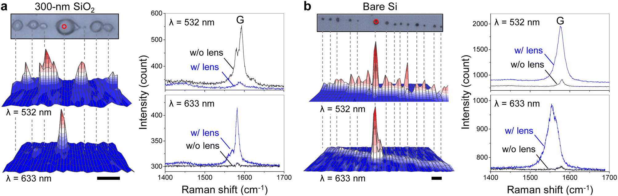 | ||
| Fig. 4 Modulation of Raman scattering of SWNTs by interference lenses. (a) Optical image of a SWNT decorated with NaCl lenses (top) on a 300 nm SiO2/Si substrate, corresponding Raman map of G-band of nanotubes at 532 nm (middle) and 633 nm (bottom) laser excitations, and individual spectra (right), obtained from the spot indicated by red circle, with (blue) and without (blue) the lens. (b) The same measurements shown in (a) repeated with another SWNT on a bare silicon substrate. Scale bars: 4 μm. | ||
Similarly, the interference lens also enhanced the Raman scattering of a graphene sheet on a SiO2/Si substrate. Compared to the carbon nanotube, the 2D nanostructure permitted the placement of a relatively large lens (d = 5 μm), within which the circular fringe patterns were clearly observable in the Raman map (Fig. S9†). We also expect the lens to enable characterization of graphene on a bare silicon substrate, which normally exhibits weak Raman signal in the absence of interference effect,4 such as a graphene-silicon Schottky diode platform for applications in photodetection,41 solar energy harvesting,42 and gas sensors.43 The results above suggest that the local modulation of Raman scattering by the salt lens is governed strongly by the interference conditions and thus applies to characterization of various nanomaterials.
Experimental
Sample preparation
Droplets of LiCl (3 M) were placed on silicon substrates having various oxide-layer thicknesses (bare, 150, and 300 nm). The thickness of the SiO2 layer was measured using ellipsometry (Elli-SE-UaM8, Elipso Technology). Surface roughness values for the silicon substrates were obtained using atomic force microscopy (MultiMode 8 system, Bruker).Raman spectroscopy and mapping
Raman spectroscopy was performed using a WITec Alpha 300 instrument equipped with 532- and 633 nm excitation lasers, through a 100× objective (Olympus MplanFL N, NA 0.9). All spectra were obtained at its maximum intensity.Decoration of salt micro/nanolens array along carbon nanotubes by exterior transport
Horizontally aligned carbon nanotubes were synthesized and decorated with salt micro/nanolenses as we reported previously.29 Briefly, a 30 nm-thick Pt metal cover was deposited on the substrate, perpendicular to the nanotubes, to apply the bias with respect to the ionic solution. Then, a millimeter-wide strip of photoresist was patterned on the metal cover. Nanotubes unprotected by the photoresist were etched using reactive ion etching (RIE), at 20 sccm O2 and 100 mTorr for 1 min, and then, the photoresist was removed using acetone. A droplet of 3 M NaCl solution was then placed on the etched area. Silanol groups created by RIE made the area hydrophilic and ensured that the droplets were in contact with the nanotubes. One Pt wire from the (+) side was dipped into the ionic droplet and another Pt wire from the (−) side was in contact with the metal cover. Then, an electrical bias was applied using a direct-current (DC) power supply (GwInstek, GPR-30H10D).Conclusions
We demonstrated interference micro/nanolenses of hygroscopic salts that locally modulate Raman scattering of various specimens including nanomaterials. The Raman scattering of the specimen beneath the plano-convex salt lens was determined by the diameter of the lens as well as interference conditions, such as wavelength of excitation laser and oxide thickness of the substrate. The Raman intensity map obtained from the lens was closely correlated with Newton rings within each lens, which enabled local modulation of Raman scattering of graphene and carbon nanotube. Our study highlights the role of interference in Raman spectroscopy of nanomaterials, and implies broad applications of the interference micro/nanolenses in spectroscopic characterization of nanomaterials and molecular species.Conflicts of interest
The authors declare no conflict of interest.Acknowledgements
This research was supported by the Basic Science Research Program through the National Research Foundation (NRF) of Korea (2022R1C1C2013306) and the Institute of Civil Military Technology Cooperation Center funded by the Defense Acquisition Program Administration and Ministry of Trade, Industry and Energy, and of Korean government under grant no. 20-CM-BR-05. This study contains results obtained at the UNIST Central Research Facilities (UCRF).References
- P. Blake, E. W. Hill, A. H. Castro Neto, K. S. Novoselov, D. Jiang, R. Yang, T. J. Booth and A. K. Geim, Appl. Phys. Lett., 2007, 91, 063124 CrossRef.
- C. Casiraghi, A. Hartschuh, E. Lidorikis, H. Qian, H. Harutyunyan, T. Gokus, K. S. Novoselov and A. C. Ferrari, Nano Lett., 2007, 7, 2711–2717 CrossRef CAS PubMed.
- Y. Y. Wang, Z. H. Ni, Z. X. Shen, H. M. Wang and Y. H. Wu, Appl. Phys. Lett., 2008, 92, 043121 CrossRef.
- D. Yoon, H. Moon, Y. W. Son, J. S. Choi, B. H. Park, Y. H. Cha, Y. D. Kim and H. Cheong, Phys. Rev. B: Condens. Matter Mater. Phys., 2009, 80, 125422 CrossRef.
- L. B. Gao, W. C. Ren, B. L. Liu, R. Saito, Z. S. Wu, S. S. Li, C. B. Jiang, F. Li and H. M. Cheng, Acs Nano, 2009, 3, 933–939 CrossRef CAS PubMed.
- X. Ling and J. Zhang, J. Phys. Chem. C, 2011, 115, 2835–2840 CrossRef CAS.
- S. Pahlow, T. Mayerhofer, M. van der Loh, U. Hubner, J. Dellith, K. Weber and J. Popp, Anal. Chem., 2018, 90, 9025–9032 CrossRef CAS PubMed.
- X. H. Zhang, J. M. Ren, H. J. Yang, Y. H. He, J. F. Tan and G. G. Qiao, Soft Matter, 2012, 8, 4314–4317 RSC.
- H. J. Yang, S. H. Peng, X. T. Hao, T. A. Smith, G. G. Qiao and X. H. Zhang, Soft Matter, 2014, 10, 957–964 RSC.
- X. Zhang, J. Wang, L. Bao, E. Dietrich, R. C. A. van der Veen, S. Peng, J. Friend, H. J. W. Zandvliet, L. Yeo and D. Lohse, Soft Matter, 2015, 11, 1889–1900 RSC.
- H. Cha, J. C. Ma, Y. S. Kim, L. N. Li, L. W. Sun, J. S. Tong and N. Miljkoyic, Acs Nano, 2019, 13, 13343–13353 CrossRef CAS PubMed.
- B. P. Dyett, M. Li, H. Zhao and X. Zhang, J. Phys. Chem. C, 2019, 123, 29866–29874 CrossRef CAS.
- J. Qian, G. F. Arends and X. Zhang, Langmuir, 2019, 35, 12583–12596 CrossRef CAS PubMed.
- T. Georgiou, L. Britnell, P. Blake, R. V. Gorbachev, A. Gholinia, A. K. Geim, C. Casiraghi and K. S. Novoselov, Appl. Phys. Lett., 2011, 99, 093103 CrossRef.
- Y. Huang, X. Wang, X. Zhang, X. Chen, B. Li, B. Wang, M. Huang, C. Zhu, X. Zhang and W. S. Bacsa, Phys. Rev. Lett., 2018, 120, 186104 CrossRef CAS PubMed.
- M. S. Dresselhaus, A. Jorio, M. Hofmann, G. Dresselhaus and R. Saito, Nano Lett., 2010, 10, 751–758 CrossRef CAS PubMed.
- J. Y. Lee, B. H. Hong, W. Y. Kim, S. K. Min, Y. Kim, M. V. Jouravlev, R. Bose, K. S. Kim, I. C. Hwang, L. J. Kaufman, C. W. Wong, P. Kim and K. S. Kim, Nature, 2009, 460, 498–501 CrossRef CAS.
- E. McLeod, C. Nguyen, P. Huang, W. Luo, M. Veli and A. Ozcan, Acs Nano, 2014, 8, 7340–7349 CrossRef CAS PubMed.
- J. X. Li, W. Gao, R. F. Dong, A. Pei, S. Sattayasamitsathit and J. Wang, Nat. Commun., 2014, 5, 5026 CrossRef CAS PubMed.
- O. Mudanyali, E. McLeod, W. Luo, A. Greenbaum, A. F. Coskun, Y. Hennequin, C. P. Allier and A. Ozcan, Nat. Photonics, 2013, 7, 247–254 CrossRef PubMed.
- D. Kang, C. Pang, S. M. Kim, H. S. Cho, H. S. Um, Y. W. Choi and K. Y. Suh, Adv. Mater., 2012, 24, 1709–1715 CrossRef CAS PubMed.
- S. Nagelberg, L. D. Zarzar, N. Nicolas, K. Subramanian, J. A. Kalow, V. Sresht, D. Blankschtein, G. Barbastathis, M. Kreysing, T. M. Swager and M. Kolle, Nat. Commun., 2017, 8, 14673 CrossRef PubMed.
- J. H. Park, C. Park, H. Yu, J. Park, S. Han, J. Shin, S. H. Ko, K. T. Nam, Y. H. Cho and Y. Park, Nat. Photonics, 2013, 7, 455–459 CrossRef.
- J. H. Yun, E. Lee, H. H. Park, D. W. Kim, W. A. Anderson, J. Kim, N. M. Litchinitser, J. W. Zeng, J. S. Yi, M. M. D. Kumar and J. B. Sun, Sci. Rep., 2014, 4, 6879 CrossRef CAS PubMed.
- Y. C. Li, X. S. Liu, X. G. Yang, H. X. Lei, Y. Zhang and B. J. Li, Acs Nano, 2017, 11, 10672–10680 CrossRef CAS PubMed.
- I. Alessandri, N. Bontempi and L. E. Depero, RSC Adv., 2014, 4, 38152–38158 RSC.
- V. R. Dantham, P. B. Bisht and C. K. R. Namboodiri, J. Appl. Phys., 2011, 109, 103103 CrossRef.
- G. Biskos, A. Malinowski, L. M. Russell, P. R. Buseck and S. T. Martin, Aerosol Sci. Technol., 2006, 40, 97–106 CrossRef CAS.
- Y. T. Kim, H. Min, M. S. Strano, J. H. Han and C. Y. Lee, Nano Lett., 2020, 20, 812–819 CrossRef CAS PubMed.
- Y. T. Kim, D. Kim, S. Park, A. Zhexembekova, M. Byeon, T. E. Hong, J. Lee and C. Y. Lee, Adv. Opt. Mater., 2021, 9, 2101209 CrossRef CAS.
- G. Pirruccio, L. M. Moreno, G. Lozano and J. G. Rivas, Acs Nano, 2013, 7, 4810–4817 CrossRef CAS PubMed.
- R. R. Nair, P. Blake, A. N. Grigorenko, K. S. Novoselov, T. J. Booth, T. Stauber, N. M. R. Peres and A. K. Geim, Science, 2008, 320, 1308 CrossRef CAS PubMed.
- R. Ramirez-Jimenez, L. Alvarez-Fraga, F. Jimenez-Villacorta, E. Climent-Pascual, C. Prieto and A. de Andres, Carbon, 2016, 105, 556–565 CrossRef CAS.
- X. L. Yin, Y. L. Li, F. Ke, C. F. Lin, H. B. Zhao, L. Gan, Z. T. Luo, R. G. Zhao, T. F. Heinz and Z. H. Hu, Nano Res., 2014, 7, 1613–1622 CrossRef CAS.
- Y. C. Lee, E. Y. Wang, Y. L. Liu and H. L. Chen, Chem. Mater., 2015, 27, 876–884 CrossRef CAS.
- I. H. Abidi, A. A. Cagang, A. Tyagi, M. A. Riaz, R. Z. Wu, Q. P. Sun and Z. T. Luo, RSC Adv., 2016, 6, 7093–7100 RSC.
- J. Y. Huang, Y.-C. Lo, J. J. Niu, A. Kushima, X. Qian, L. Zhong, S. X. Mao and J. Li, Nat. Nanotechnol., 2013, 8, 277–281 CrossRef CAS PubMed.
- K. Yum and M.-F. Yu, Phys. Rev. Lett., 2005, 95, 186102 CrossRef PubMed.
- Y. T. Kim, S. H. Joo, H. Min, J. Lee, S. M. Moon, M. Byeon, T. E. Hong, M. S. Strano, J. H. Han, S. K. Kwak and C. Y. Lee, Chem. Mater., 2018, 30, 5184–5193 CrossRef CAS.
- C.-C. Chang, I. K. Hsu, M. Aykol, W.-H. Hung, C.-C. Chen and S. B. Cronin, Acs Nano, 2010, 4, 5095–5100 CrossRef CAS PubMed.
- X. An, F. Liu, Y. J. Jung and S. Kar, Nano Lett., 2013, 13, 909–916 CrossRef CAS PubMed.
- X. Miao, S. Tongay, M. K. Petterson, K. Berke, A. G. Rinzler, B. R. Appleton and A. F. Hebard, Nano Lett., 2012, 12, 2745–2750 CrossRef CAS PubMed.
- H.-Y. Kim, K. Lee, N. McEvoy, C. Yim and G. S. Duesberg, Nano Lett., 2013, 13, 2182–2188 CrossRef CAS PubMed.
Footnote |
| † Electronic supplementary information (ESI) available. See DOI: https://doi.org/10.1039/d3ra05722d |
| This journal is © The Royal Society of Chemistry 2023 |