
 Open Access Article
 This Open Access Article is licensed under a Creative Commons Attribution-Non Commercial 3.0 Unported Licence
Nano-scale smooth surface of the compact-TiO2 layer via spray pyrolysis for controlling the grain size of the perovskite layer in perovskite solar cells†
Methawee Nukunudompanich‡
 ,
Kazuma Suzuki,
Keisuke Kameda,
Sergei Manzhos and
Manabu Ihara*
,
Kazuma Suzuki,
Keisuke Kameda,
Sergei Manzhos and
Manabu Ihara*
Department of Chemical Science and Engineering, Tokyo Institute of Technology, 152-8552, Tokyo, Japan. E-mail: mihara@chemeng.titech.ac.jp
First published on 18th September 2023
Abstract
The mechanism of perovskite film growth is critical for the final morphology and, thus, the performance of the perovskite solar cell. The nano-roughness of compact TiO2 (c-TiO2) fabricated via the spray pyrolysis method had a significant effect on the perovskite grain size and perovskite solar cell performance in this work. While spray pyrolysis is a low-cost and straightforward deposition technique suitable for large-scale application, it is influenced by a number of parameters, including (i) alcoholic solvent precursor, (ii) spray temperature, and (iii) annealing temperature. Among alcoholic solvents, 2-propanol and 1-butanol showed a smooth surface without any large TiO2 particles on the surface compared to EtOH. The lowest roughness of the c-TiO2 layer was obtained at 450 °C with an average perovskite grain size of around 300 nm. Increased annealing temperature has a positive effect on the roughness of TiO2. The highest efficiency of the solar cell was achieved by using 1-butanol as the solvent. The decrease in the nano roughness of c-TiO2 promoted larger perovskite grain sizes via a relative decrease in the nucleation rate. Therefore, controlling the spray pyrolysis technique used to deposit the c-TiO2 layer is a promising route to control the surface nanoroughness of c-TiO2, which results in an increase in the MAPbI3 grain size.
1 Introduction
Recent developments in the field of perovskite solar cells (PSC) have been promising with the record power conversion efficiency (PCE) having surpassed 26%.1,2 The possibility of using a wet fabrication process is particularly attractive for scalable production. A PSC generally consists of a transparent electrode, an electron transport layer (ETL), a perovskite absorber, a hole transport layer (HTL), and a counter electrode. The device types are classified in n-i-p or inverted p-i-n based on the charge transport layer assembly.3 The perovskite layer in first PSCs4 was deposited on a mesoporous metal oxide, similar to the structure of a dye-sensitized solar cell, which also contains a mesoporous metal oxide and a liquid electrolyte. That configuration has since been abandoned in favor of planar configurations with a perovskite layer on top of a flat and compact inorganic ETL such as TiO2, SnO2, ZnO, and others.5 In PSCs, the most frequently employed ETL types are crystalline (c-TiO2) and fullerenes. Titania based ETLs have the disadvantage of requiring relatively high processing temperatures which many believe disadvantages them in terms of scalability and cost. On the other hand, titania ETLs allow obtaining high efficiencies. Development of titania ETL fabrication processes that combine ease of fabrication while providing high PCE and other cell performance parameters (fill factor, open circuit voltage, short-circuit current) remains therefore an important issue.In planar PSCs, the morphology of the selected contacts and interfaces between the layers influences the entire cell performance, including the PCE. Numerous deposition processes exist for thin film c-TiO2, including dip- or spin-coating,6 spray-pyrolysis,7 the doctor blade method,8 pulsed laser deposition (PLD),6 magnetron sputtering,7 electrochemical approaches, and atomic layer deposition (ALD).9 Spray-pyrolysis is a low-cost, high-productivity process that permits uniform coating on a variety of substrate sizes and shapes. It overcomes the limitations of the ALD growth method by using an inorganic salt precursor solution. When spraying, the spray pyrolysis mechanisms10 control solvent droplet drying and precipitation of the precursor as well as vaporization. While this method is easy to set up and inexpensive, the final characteristics of the thin film achieved with it depend on several parameters,11 including the distance between the spray nozzle and the substrate, the pyrolysis temperature, the spray duration, the spray flow rate, the precursor solvent, and concentration. Thus, each parameter must be precisely controlled to ensure reproducible thin film results. Importantly, the morphology of the obtained titania film influences the properties of the perovskite layer. In this work we show that tuning precursor chemistry in spray pyrolysis is a promising approach for optimizing the material properties of c-TiO2 layers used as ETLs in hybrid PSC to improve photovoltaic conversion efficiency. In particular, we show that in this way the grain size of the perovskite film grown on top of c-TiO2 can be controlled and improved achieving larger perovskite grains which have been shown to be desired in PSCs.12–19
It is vital to consider the crystallographic properties of the active materials of any type of semiconductor solar cell while attempting to get a high PCE. The best way to get a high PCE in Si solar cells is to make monocrystalline Si with few impurities and/or defects and adequate surface passivation. The PCE of polycrystalline Si solar cells (500 μm grain size) is limited by the role of grain boundaries (GBs) as recombination centers.20 Single-crystals would be ideal because of lack of any GBs and hence low trap density. Several approaches to increase grain sizes and to make quasi-single crystals were proposed,21–24 because the grain size and GBs are among the main factors that determine the photoelectric conversion efficiency. In comparison to Si solar cells, solution-grown MAPbI3 films in PSCs are polycrystalline and have a high number of GBs. GBs have the potential to operate as recombination centers, hence lowering PCE of PSCs.25,26 Numerous researches have been conducted to determine how the crystallographic properties of the perovskite layer affect the performance of the cell. Large, high-quality crystals grow slowly and with little supersaturation – this encourages three-dimensional growth and diminishes the regularity and continuity of thin films. It is necessary to disentangle the effects of grain size and GBs on cell performance. For PSCs, it is crucial to control nucleation and crystal growth. Additionally, GBs are susceptible to degradation because of their high sensitivity to moisture, heat, and light. The influence of GBs on the performance of PSCs can be reduced by (1) passivating at GB,13,14 (2) increasing the average grain size to decrease the concentration of GB,15 and (3) improving perovskite grain quality through the addition of additives or optimization of precursor ratios.16 Passivating MAPbI3 with Na+ or K+ has been shown by Zhao et al.14 Huang et al.15 increased the perovskite layer annealing temperature to improve MAPbI3 particle size. A low annealing temperature caused crystal defects and remaining solvent molecules in the perovskite layer. Kim et al.16 investigated the effect of PbI2/MAI ratio on perovskite film manufacturing to improve perovskite grain quality. Some faster methods for generating a homogeneous solid film followed by thermal annealing exist. Flat-surface perovskites were made antisolvent by Ahn et al.21 A solid perovskite film or an intermediate compound phase can be made by rapidly removing the solvent from the film and then annealing it. As explained above, the effect of the grain size is accompanied by other effects, such as (1) quality of the grains,16 (2) passivation at the GBs,14,15 (3) thickness of the perovskite film17 and (4) inner interfaces of mesoporous TiO2.18
We have previously shown19 that perovskite grain sizes can be controlled by altering the roughness of TiO2 on the nanoscale. With low roughness, a wide range of grain sizes is achievable without modifying the materials or the perovskite structure. The direct dominant effect of the MAPbI3 grain size on the PSC performance was clearly revealed, in which the grain quality and the MAPbI3 layer thickness were maintained and imperfections such as void formation were prevented at the interface of flat TiO2. However, the mechanism of control of the perovskite grain size by surface roughness of TiO2 was unclear. In this paper, we analyse this mechanism.
We control the surface roughness (Rms) of c-TiO2 in this study by adjusting the spray pyrolysis process without using extra parameters. To control the surface roughness of c-TiO2, we evaluated the spray pyrolysis parameters as a function of solvent and temperature, including solvents (ethanol, isopropanol, and 1-butanol), spray temperature (Ts) and annealing temperature (Ta). The spray pyrolysis parameters have a significant effect on the MAPbI3 grain sizes. Additionally, in this work, the mechanism to control grain sizes of the perovskite was proposed and the relationship between the roughness of c-TiO2 and MAPbI3 grain size was studied. The influence of nano-roughness of c-TiO2 can be described using the nucleation theory.
2 Experimental
2.1 Spray pyrolysis
The spray pyrolysis19,24 process was set up (Fig. 1) used to deposit a c-TiO2 layer on indium-doped tin oxide (ITO). To begin, ITO glass substrates (sheet resistance: 5 Ω sq−1, Geomatec's high-temperature resistance ITO substrate) were etched with Zn dust and hydrochloric acid (HCl, 1 M), and then cleaned sequentially for 20 minutes with detergent, de-ionized water, and ethanol. Additionally, ITO glass surfaces were treated for 1 hour to ultraviolet (UV)/ozone radiation. Firstly, the spray height and angle were varied as indicated in Fig. 1b. Then, using varied spray temperatures (Ts = 350, 450, or 550 °C), a c-TiO2 layer was formed on the ITO using the spray pyrolysis method. The 0.15 M c-TiO2 solution was prepared by dissolving 2.5 ml titanium diisopropoxide bis(acetylacetonate) (TiAcAc) solution (Sigma-Aldrich) in 20 ml ethanol, 2-propanol, or 1-butanol (TCI). Following that, samples were annealed for 1 hour at various annealing temperatures (Ta = 400, 450, 500, or 600 °C) to eliminate organic components and enhance the crystallization quality of the c-TiO2 thin film. | ||
| Fig. 1 Schematic of (a) the lab-scale spray coating equipment, (b) spraying angle adjustment (45°, 90°) and height optimization (30, 40, 50 cm). | ||
2.2 Perovskite solar cell fabrication
The planar PSC device structure was fabricated using an ITO glass substrate as a bottom electrode, a c-TiO2 layer as an ETL by spray pyrolysis as described previously, a light-absorbing perovskite layer (MAPbI3), 2,2′,7,7′-tetrakis{N,N-di(4-methoxyphenyl)amino}-9,9′-spirobifluorene (Spiro-OMeTAD, Merck) as an HTL, and a top Au electrode deposited by thermal evaporation. After the c-TiO2 layer on the ITO substrate was cooled to room temperature, a one-step method developed by Ahn N. et al.,17 was used with 422 mg of PbI2, 159 mg of MAI, and 78 mg of DMSO (molar ratio 1![[thin space (1/6-em)]](https://www.rsc.org/images/entities/char_2009.gif) :1:1) as perovskite precursor. Then, raw materials were mixed in 600 mg of DMF solution and stirred for one hour at room temperature. The perovskite was spin-coated onto the compact TiO2 layer at 5000 rpm for 30 s with 300 μl of diethyl ether as an antisolvent solution. Then the samples were annealed at 100 °C for 30 min. Next, the spiro-OMeTAD solution was prepared by using 80 mg spiro-OMeTAD, 22.5 ml 4-tertbutylpyridine (Sigma-Aldrich) and 17.5 ml lithium bis(trifluoromethane sulfonyl)imide (Li-TFSI, Sigma-Aldrich) solution (520 mg Li-TFSI in 1 ml acetonitrile) in 1 ml chlorobenzene, and then spin-coating the resulting solution onto the perovskite layer at 3000 rpm for 30 s. Finally, Au was deposited on this HTL by thermal vacuum evaporation as a top electrode.
:1:1) as perovskite precursor. Then, raw materials were mixed in 600 mg of DMF solution and stirred for one hour at room temperature. The perovskite was spin-coated onto the compact TiO2 layer at 5000 rpm for 30 s with 300 μl of diethyl ether as an antisolvent solution. Then the samples were annealed at 100 °C for 30 min. Next, the spiro-OMeTAD solution was prepared by using 80 mg spiro-OMeTAD, 22.5 ml 4-tertbutylpyridine (Sigma-Aldrich) and 17.5 ml lithium bis(trifluoromethane sulfonyl)imide (Li-TFSI, Sigma-Aldrich) solution (520 mg Li-TFSI in 1 ml acetonitrile) in 1 ml chlorobenzene, and then spin-coating the resulting solution onto the perovskite layer at 3000 rpm for 30 s. Finally, Au was deposited on this HTL by thermal vacuum evaporation as a top electrode.
2.3 Characterization
The surface and cross-section morphologies and film thickness of c-TiO2 and perovskite films were obtained using a field emission scanning electron microscope (FESEM, JEOL JSM-7001F). The surface roughness of c-TiO2 and perovskite film were measured by atomic force microscopy (AFM, multimodal N3-IHA SPM system). Water wettability of the c-TiO2 layer was determined using digital image analysis of water droplet shapes. The large TiO2 particle on the c-TiO2 surface or grain size data were extracted from the SEM image using ImageJ software. The X-ray diffraction (XRD, Rigaku Japan) patterns were recorded using Cu Kα radiation (λ = 1.5418 Å). The J–V characteristics of the PSCs were measured (CEP-2000ML, Bunkoukeiki) using a solar simulator and a source meter (Keithley 2400). The AM 1.5 illumination of 100 mW cm−2 was calibrated based on a standard Si reference cell. A scan rate of 150 mV s−1 was used, from short circuit to forward bias and then in reverse scan. An active area is 0.54 cm2 using a shadow mask of the same area.3 Results
3.1 Effect of substrate temperature, and annealing temperature, on surface roughness and crystallinity of TiO2
Fig. 2a–c examines the influence of substrate temperature (Ts) and annealing temperature (Ta) on the root mean square (Rms) values of the surface roughness and the crystallinity of c-TiO2. The data obtained from nanoscale morphology analysis using FESEM and Rms measurements from AFM highlight the changing morphology and Rms values with Ts. Increasing Ts from 350 °C to 550 °C alters the morphology of the TiO2 thin film because the properties of 1-butanol, including density and surface tension, promote the formation of smaller droplets at higher temperatures (450–550 °C). Solvents with low boiling points (Tb) easily evaporate, impacting the success of pyrolysis. However, at lower temperatures (350 °C), droplets directly contact the substrate without undergoing additional processes like vaporization and precipitation. This leads to the splattering of aerosol particles on the surface, resulting in the precipitation believed to be an amorphous salt Ti[OH]4. Subsequent decomposition and oxidation give rise to a non-uniform TiO2 structure on the thin film surface. This phenomenon is referred to as the “coffee ring structure” and is caused by the differential evaporation rates of the precursor at the droplet's edge and center. Because at the droplet's edge are evaporated more quickly. This causes liquid to retreat from the edges, leaving a ring-shaped deposit behind. As shown in Fig. 2c, when measuring Rms from low-temperature spray pyrolysis, low and high Rms areas were observed”.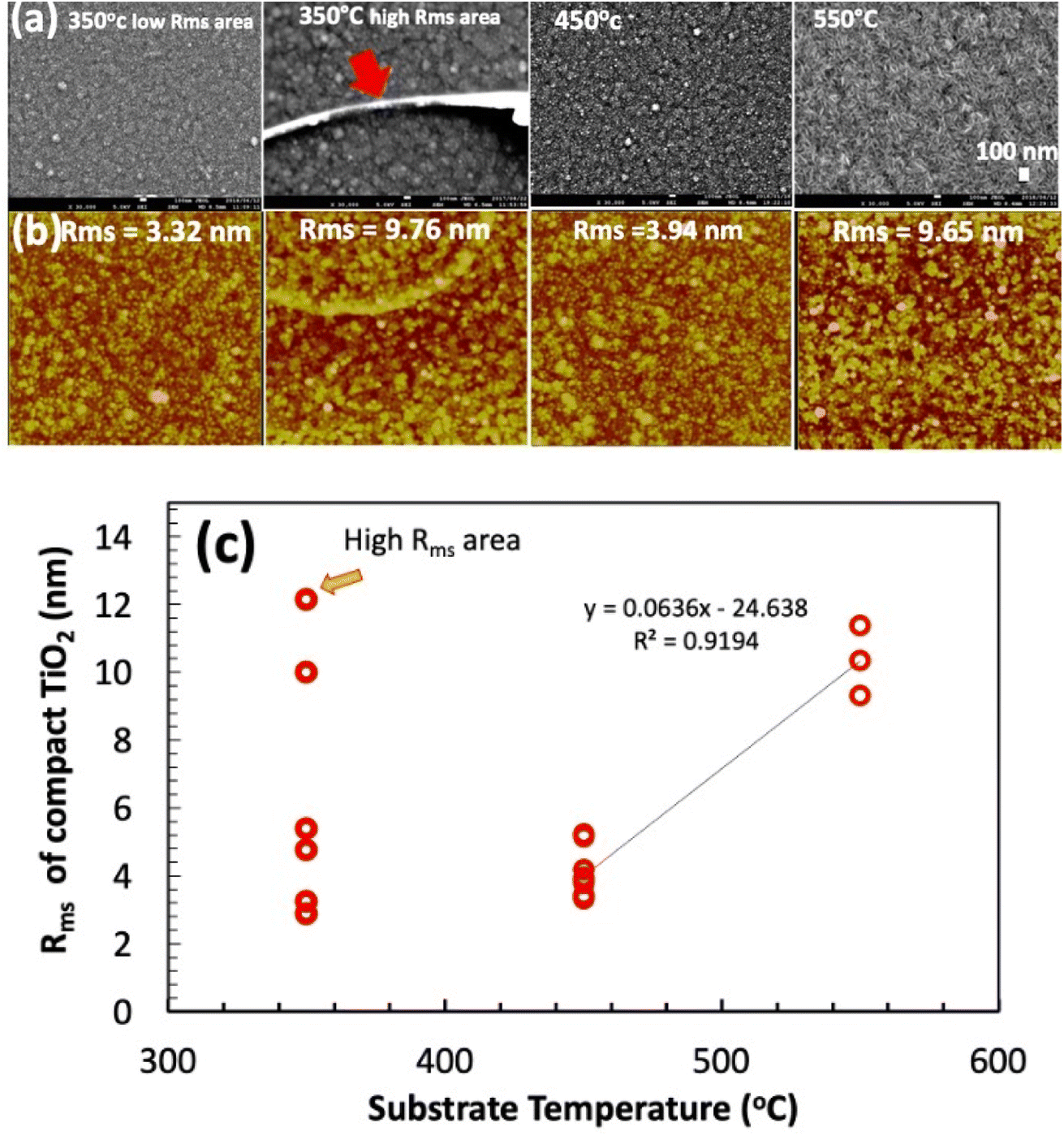 | ||
| Fig. 2 Effect of spray temperature Ts on (a) SEM surface images of c-TiO2 layer and (b) AFM image of Rms of c-TiO2 at different Ts = 350 (denoted as low Rms and high Rms area), 450, and 550 °C. The measurement area is 5 × 5 μm, (c) Relationship between Rms of c-TiO2 and Ts. | ||
To verify the effect of annealing temperature or Ta, an extensive examination of film roughness and morphology was conducted using SEM and AFM characterization. Fig. 3a showcases SEM images of the c-TiO2 film, which was prepared using 1-butanol as the solvent and annealed at Ta = 400 °C, at various Ts of 350, 450, and 550 °C. Correspondingly, Fig. 3b presents AFM images (5 × 5 μm) of the samples obtained under each condition. The relationship between Rms and Ts is depicted in Fig. 3c, while Fig. 3d illustrates the distribution of perovskite grain sizes. For Ts values of 350, 450, and 550 °C, the Rms values of the c-TiO2 layers ranged from 5 nm to 12 nm, 3 nm to 6 nm, and 9 nm to 12 nm, respectively. Notably, the lowest Rms value for the c-TiO2 film was achieved at Ts = 450 °C, which met the criteria for generating TiO2 nanoparticles and yielded a c-TiO2 film devoid of surface impurities. The grain size distribution of MAPbI3 (perovskite) was approximately 250–300 nm at Ts = 350 °C and 450 °C, while it reduced to around 200 nm at Ts = 550 °C. As Ts increased, the grain size distribution of MAPbI3 exhibited a decrease in size (as observed in Fig. 3c).
 | ||
| Fig. 3 Effect of the annealing temperature Ta on (a) SEM surface images of c-TiO2 layer and (b) AFM image of c-TiO2 at different Ta = 400, 450, 500 and 600 °C with the measurement area of 5 × 5 μm, and (c) relationship between the surface roughness Rms and Ta. | ||
Table 1 provides a summary of the experimental control conditions for the respective TiO2 roughness and spray patterns. The spray angle was optimized between 45° and 90° (No. 1–2 in Table 1), showing that a 45° angle resulted in a non-uniform c-TiO2 film thickness due to variations in nozzle-substrate distances (condition no. 1). Here, we defined spray patterns as A: ring pattern; B: numerous large particles; C: uniform flat film; and D: inadequate coverage with a small particle film. Pattern A was identified as the dominant mechanism based on optical and FESEM images (Table S1†). High-resolution FESEM imaging revealed ring formation during spray pyrolysis due to different vaporization rates at different distances of the nozzle to the substrate. A 90° spray angle provided greater uniformity, enabling uniform droplet deposition. AFM analysis measured Rms as 9.76 nm and 4.25 nm for 45-degree and 90-degree angles, respectively.
| No. | Substrate temperature (Ts, °C) | Solvents | Boiling point (Tb, °C) | Distance (cm) | Spray angle (°) | Annealing temperature (Ta, °C) | Rms (nm) | Type of spray mechanism | Grain size of TiO2 (nm) |
|---|---|---|---|---|---|---|---|---|---|
| a Note: type of pattern referred as A: ring pattern; B: many large particles; C: homogeneous flat film; D: poor coverage with small particle film. The spray mechanism for each condition was determined by using optical microscope and FESEM images as indicated in Fig. S1–S3. | |||||||||
| 1 | 350 | Ethanol | 78 | 30 | 45 | 400 | 9.76 (non-uniform film) | A | 276.5 |
| 2 | 90 | 4.25 | B | 243.75 | |||||
| 3 | 40 | 7.87 | C (poor coverage film) | 276 | |||||
| 4 | 50 | 3.32 | A (poor coverage) | Hardly observed | |||||
| 5 | 30 | 4.12 | A | 200 | |||||
| 6 | Propanol | 82 | 3.76 | A | 96.3 | ||||
| 7 | Butanol | 117 | 6.75 | B | 205.4 | ||||
| 8 | 450 | Ethanol | 78 | 43.51 | B | 239.3 | |||
| 9 | Propanol | 82 | 5.01 | C | 46 | ||||
| 10 | Butanol | 117 | 3.94 | C | 189.4 | ||||
| 11 | 550 | Ethanol | 78 | 26.66 | D | 323.3 | |||
| 12 | Propanol | 82 | 4.17 | D | 80.8 | ||||
| 13 | Butanol | 117 | 9.65 | C | 164 | ||||
| 14 | 450 | 4.12 | B | 246.8 | |||||
| 15 | 450 | 4.88 | C | 190.9 | |||||
| 16 | 500 | 5.23 | C | 73.4 | |||||
| 17 | 600 | 7.88 | C | 117.5 | |||||
Next, the effect of spray distance between the nozzle and substrate was investigated while maintaining constant concentration and substrate temperature. Spray distances of 30 40, and 50 cm (No. 2, 3, and 4 in Table 1) were examined. FESEM and XRD measurements determined surface roughness and crystalline size of TiO2, respectively. Surface roughness at 30, 40, and 50 cm spray distances were 4.25, 7.84, and 3.32 nm, respectively. The lowest Rms value (3.32 nm) at 50 cm was attributed to poor TiO2 deposition on ITO, resulting in measurement of the ITO layer rather than TiO2. Thus, a spray distance of 30 cm was determined as optimal, ensuring complete coverage and a uniform film.
Subsequently, the TiO2 precursor solvent was changed from EtOH to 2-propanol or 1-butanol to examine the effect of solvent Tb on c-TiO2 roughness and film morphology (No. 5–7 in Table 1). EtOH, 2-propanol, and 1-butanol have Tb of 78, 82, and 117 °C, respectively. 2-propanol exhibited the lowest Rms value (3.76 nm) among the solvents. However, SEM images (Fig. S3 in ESI†) showed a coffee ring morphology for all solvents and conditions, attributed to droplet spreading at low substrate temperatures in line with spray pyrolysis pattern A.
The XRD patterns of as-prepared and annealed (Ta = 400, 500, and 600 °C) c-TiO2 samples are shown in Fig. 4. Fig. 4a illustrates diffraction peaks associated with the (101), (103), (200), and (105) crystal planes of anatase phase of TiO2, as well as a trace of rutile phase (JCPDS card no. 01-084-1285). The Full-Width Half Maximum (FWHM) of the anatase reflections A1 (101), A2 (103), and A3 (105) indicate highly crystalline c-TiO2 (Fig. 4b). The calculated FWHM value and its correlation with the degree of crystallinity of the c-TiO2 layer are shown in Table 2. The phase structure of c-TiO2 on an ITO substrate after 400 °C annealing demonstrates decreased crystallinity. When the sample was annealed at Ta = 500 and 600 °C, the diffraction pattern revealed strong intensities corresponding to the characteristic peaks of anatase phase. The FWHM value can provide information about the structural properties of a material in relation to the degree of crystallinity of a c-TiO2 layer. Atoms in crystalline substances, such as c-TiO2, are arranged in a regular, repeating pattern. This arrangement produces well-defined peaks in X-ray and electron diffraction patterns. More crystallinity corresponds to a narrower FWHM, indicating a more ordered and well-defined crystal structure. This is because the diffraction peaks in highly crystalline materials are sharper and more distinct, resulting in a smaller FWHM value. A wider FWHM, on the other hand, indicates a higher degree of disorder or the presence of defects, such as grain boundaries, dislocations, or lattice distortions. Crystalline regions diffract X-rays or electrons coherently, whereas amorphous or less ordered regions scatter the radiation incoherently. The presence of disorder or imperfections in the crystal structure leads to a broadening of the diffraction peaks and, consequently, an increase in the FWHM value.
 | ||
| Fig. 4 XRD patterns showing the effect of (a) Ta on c-TiO2 deposited on ITO at 400, 500, and 600 °C, and (b) FWHM of anatase (A) and rutile (R) in c-TiO2 layer. | ||
| Annealing temperature (Ta, °C) | A1 (2theta, °) | R1 (2theta, °) | A2 (2theta, °) | A3 (2theta, °) | Effective average crystalline grain size of anatase (nm) |
|---|---|---|---|---|---|
| 400 | 8.706 | 9.43 | 62.033 | 0.5193 | 0.955 |
| 500 | 2.433 | 10.199 | 0.274 | 0.383 | 3.416 |
| 600 | 0.201 | 0.00001 | 12.826 | 12.374 | 41.191 |
3.2 Effect of solvent on the surface roughness of TiO2
The box plot in Fig. 5 depicts the Rms of c-TiO2, which was prepared in three different solvents: EtOH, IPA, and 1-butanol. c-TiO2 films fabricated with various alcoholic solvents with different Tb and at Ts = 350, 450, and 550 °C exhibited a variety of TiO2 structural shapes, as illustrated in Fig. S1.† On many occasions, particularly when EtOH was used as a solvent, large particles and/or coffee ring structures were observed on the surface. These large TiO2 particles may act as the initial point of discontinuity in the perovskite film, eventually resulting in pinholes. In comparison, when IPA or 1-butanol is used, the surface appears to have fewer particles. When 1-butanol was used as a solvent, the roughness was the lowest. Additionally, the relationship between the average amount of large and submicron TiO2 particles on the surface and the solvent type in Fig. S2† indicated that EtOH had the highest numbers of large TiO2 particles on the surface, which was consistent with the above findings. When EtOH was used as a TiO2 precursor solvent, the SEM images in Fig. S3† also revealed large TiO2 particles on the surface. The large TiO2 particles generated by spraying alkoxide solutions19 create a discontinuous and rough surface on the c-TiO2 films. | ||
| Fig. 5 Relationship between surface roughness Rms and c-TiO2 from different solvent when Ts = 450 °C and Ta = 450 °C. | ||
3.3 Proposed mechanism to determine the morphology of TiO2
The underlying conceptual model of spray pyrolysis mechanism is derived from ref. 24. This model is based on comprehensive experiments involving various parameters such as Ts and alcoholic solvents. Fig. 6 presents a model that explains the impact of Ts and the vaporization rates of different alcoholic solvents on the final film's morphology. Assuming a constant droplet size during the spray process, this model considers standard sequences of events or reaction paths and the influence of Ts on the mechanism, including precipitation, vaporization, and powder formation. The model distinguishes four patterns (A, B, C, and D) based on the combination of Ts and vaporization rate according to the substrate temperature. At low temperatures (350 °C), the droplets directly reach the substrate without undergoing further mechanisms like vaporization and precipitation. These aerosol particles spread over the surface, leading to the precipitation of an amorphous salt (Ti[OH]4), followed by subsequent decomposition and oxidation. As a result, a non-uniform TiO2 structure forms on the thin film surface. At intermediate temperatures (450 °C), an entrainment process occurs, causing partial (higher) evaporation of the aerosol particles before reaching the substrate. These entrained particles precipitate as an amorphous salt, which then breaks down and oxidizes upon impact with the substrate. At high temperatures (550 °C), significant evaporation of the droplets takes place. The entrained aerosol particles precipitate as an amorphous salt and sublime upon contact with the substrate. The subsequent breakdown and oxidation of vapors occur at the substrate surface due to vapor transfer. At extremely high substrate temperatures, the entrained aerosol particles precipitate as an amorphous salt but sublime/oxidize well before reaching the substrate. This results in limited adhesion between the TiO2 and substrate. The determination of mechanisms A to D and the ESI Fig. S1–S3† are discussed in Table 1, as they serve as criteria for characterizing the different mechanisms involved in spray pyrolysis. | ||
| Fig. 6 Schematic of spray pyrolysis mechanism of TiO2 as a function of temperature with constant initial droplet size and vaporization rate. | ||
3.4 Relationship between perovskite grain size and the surface roughness of the TiO2 layer
In Fig. 7a, the relationship between the average perovskite grain size and the surface roughness Rms of TiO2 layer is plotted together with the data from our previous work.19 The average grain size was determined using an image processing software (ImageJ).26 In accordance with the nucleation theory,27–29 the grain size of perovskite is larger when the surface roughness of the TiO2 layer is lower. This is because a rougher surface of the TiO2 layer can provide more nucleation sites for the formation of crystalline structures. As the surface roughness increases, the available surface area for nucleation also increases, which can lead to the formation of smaller nucleation sites or grains. | ||
| Fig. 7 (a) Relationship between perovskite grain size distribution and surface roughness Rms of the TiO2 layer (annealing temperature Ta = 400 °C) and SEM images of the perovskite–titania interfaces with small MAPbI3 grain when using the spray temperature Ts = 350 °C and Ta = 450 °C (b) and large (c) MAPbI3 grain when using Ts = 450 °C and Ta = 450 °C. | ||
The effect of surface roughness on perovskite grain size is explicable in terms of grain nucleation and growth. Fig. 7 displays SEM images of the perovskite–titania interface surface and cross-sections with small and large grain sizes (Fig. 7b and c). There are no indications that 2D growth is favored in either case; grain growth remains three-dimensional in both. Consequently, the growth conditions are comparable, and the substrate has little impact. The difference lies in the nucleation conditions, which are strongly influenced by surface morphology because non-homogeneous surface regions serve as nucleation centers.
3.5 Effect of the splay pyrolysis conditions on the PCE of the cells
The efficiency of PSCs fabricated with various solvents is depicted in Fig. 8. The average PCE content of EtOH, IPA, and 1-butanol is 4%, 6%, and 9%, respectively, while the maximum PCE content is 7.0%, 10.3%, and 11.4%. When the solvent was changed from EtOH to IPA and 1-butanol, the PCEs improved. According to the previous section, EtOH has a low PCE value because large solid particles formed during spray pyrolysis act as short-circuit areas and discontinuities in the perovskite film, whereas IPA and 1-butanol have a higher PCE value due to their lower surface roughness.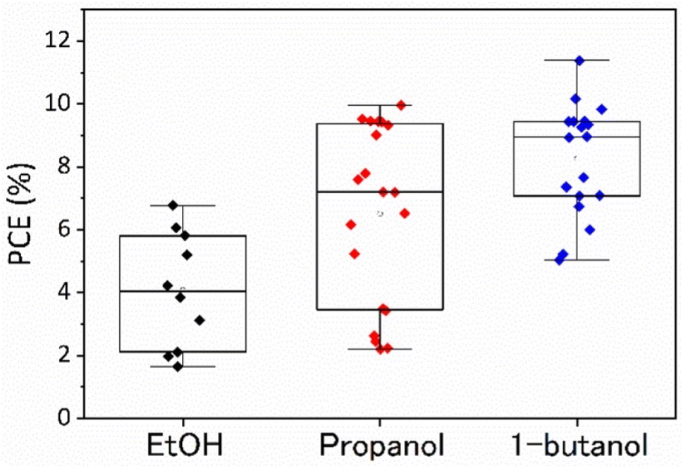 | ||
| Fig. 8 Distribution plot of power conversion efficiency (PCE) of PSC using different solvent EtOH, 2-propanol, and 1-butanol. c-TiO2 condition use Ts = 450 °C and Ta = 450 °C for all samples. | ||
3.6 Mechanism relating the perovskite grain size and the surface roughness of TiO2
The variation in the nucleation rate with surface morphology can be attributed to the differences in wetting angles. Indeed, the free energy activation barrier ΔG* for the heterogeneous nucleation on a surface can be related to the barrier of homogeneous nucleation (i.e. in the precursor solution) by introducing a shape factor (Φ),
 | (1) |
 | (2) |
Therefore, ΔG* is smaller when θ is low and larger when θ is high.
The energy barrier for heterogeneous nucleation on a flat substrate is described by eqn (1) and (2). The effect of the rough surface has been discussed theoretically as well as experimentally.25 The effect of roughness on the nucleation barrier has been modelled using cavities with a cone shape, a semi-spherical shape, or multiple cone shapes.28 Turnbull29 discussed nucleation on non-flat surfaces by examining the free energy change at the surface and the volume contained within the conical or cylindrical cavity.30,31 The surface area of the nuclei (=the interface between vapor and nuclei) decreases significantly in comparison to the flat surface, lowering the nucleation barrier. Abyzov et al. calculated the nucleation energy within a conical cavity to simulate the nucleation kinetics.30 The shape factor Φ was described with the cone angle β as follows:
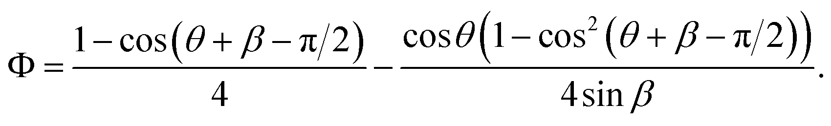 | (3) |
The Φ in eqn (3) is much smaller than that of eqn (2). When β is smaller than π/2 − θ, Φ becomes negative (the surface becomes concave) and the nuclei forms at undersaturated condition. Li et al.28 discussed the nucleation on a rough surface with multiple cavities smaller than the size of nuclei. Even when multiple conic cavities were covered with spherical nuclei, the nucleation energy became smaller. Observing the formation of larger grains is fascinating considering the heterogeneous nucleation theory. When numerous nuclei are produced, one would normally expect the grains to become smaller. In our case, where we only altered the surface energy and the Gibbs free energy change for homogeneous nucleation remained unchanged, the Gibbs free energy change for heterogeneous nucleation should be lower for a smaller contact angle.31 This is in accordance to Fig. S6.† As a result, a higher density of nuclei is present on the surface, and it is anticipated that the growth of grains will cease when they collide, resulting in a smaller grain size. According to those studies, the effect of the roughness on the nucleation density is significant at the nanometer-scale roughness. Thus, in case of the nucleation on the substrate surface, the nucleation barrier on the rough surface should be smaller than that on the smooth surface. This explains the relationship observed here between the surface roughness and the grain size.
4 Conclusions
In summary, in order to control the MAPbI3 grain size in the perovskite thin film of a perovskite solar cell, the nanometer-level surface roughness of c-TiO2 was controlled via the spray pyrolysis process which is a low-cost and straightforward deposition technique suitable for large scale production. It is affected by several parameters such as (i) alcoholic solvent precursor, (ii) spray temperature Ts, and (iii) annealing temperature Ta. For alcoholic solvents, IPA and 1-butanol show a smoother surface when compared with EtOH. A Ts of 450 °C gives the lowest roughness (Rms = 3 nm) with an average perovskite grain size around 300 nm. When Ta was varied from 400 to 600 °C, the higher Ta, the larger average grain sizes were observed. For EtOH, IPA, and 1-butanol, the average PCE of 4%, 6%, and 9%, and the highest PCE of 7%, 10.3%, and 11.4%, respectively, were obtained. The effect of Rms of c-TiO2 on the MAPbI3 grain size is explained by the classical nucleation theory. Furthermore, by controlling the roughness by the parameters of spray pyrolysis, one can fabricate devices that have larger active areas and higher PCE. Additionally, the perovskite grain size should have a large effect not only on the PCE but also the lifetime of the crystal film, so our simple approach to control the grain size of c-TiO2 is promising for further development of the fabrication process. Larger grain sizes, in turn, translate to fewer grain boundaries that can act as electronic trap states during charge transport. Therefore, the formation of a perovskite film with a smoother surface and fewer grain boundaries is highly beneficial to the photovoltaic performance.Author contributions
Methawee Nukunudompanich: conceptualization, methodology, writing – original draft, writing – review & editing. Kazuma Suzuki: formal techniques to analyze or synthesize study data. Keisuke Kameda: formal techniques to analyze or synthesize study data. Sergei Manzhos: supervision, writing – review & editing. Manabu Ihara: supervision, writing – review & editing, project administration, funding acquisition.Conflicts of interest
There are no conflicts to declare.Acknowledgements
This work was supported by JST-Mirai Program Grant Number JPMJMI22H1, Japan. M. N. thanks the Academic Metlting Pot Program (AMP 2023) of King Mongut's Intitute of Technology Ladkrabang for support (Grant no. KREF206610).References
- National renewable energy laboratory, Best research-cell efficiencies, https://www.nrel.gov/pv/cell-efficiency.html, accessed June 2023.
- A. S. Bati, Y. L. Zhong, P. L. Burn, M. K. Nazeeruddin, P. E. Shaw and M. Batmunkh, Commun. Mater., 2023, 4(1), 2 CrossRef CAS.
- Y. Zhou, X. Li and H. Lin, Small, 2019, 1902579, DOI:10.1002/smll.201902579.
- A. Kojima, K. Teshima, Y. Shirai and T. Miyasaka, J. Am. Chem. Soc., 2009, 131(17), 6050–6051 CrossRef CAS PubMed.
- S. Ratanaphan, Y. Yoon and G. S. Rohrer, J. Mater. Sci., 2014, 49(14), 4938–4945 CrossRef CAS.
- X. D. Wang, F. Shi, X. X. Gao, C. M. Fan, W. Huang and X. S. Feng, Thin Solid Films, 2013, 548, 34–39 CrossRef CAS.
- K. Wojciechowski, M. Saliba, T. Leijtens, A. Abate and H. J. Snaith, Proc. SPIE, 2014, 9184 Search PubMed.
- M. Nukunudompanich, S. Chuangchote, J. Wootthikanokkhan and Y. Suzuki, Int. Lett., 2015, 46, 30–36 Search PubMed.
- Y. Z. Wu, X. D. Yang, H. Chen, K. Zhang, C. J. Qin, J. Liu, W. Q. Peng, A. Islam, E. B. Bi, F. Ye, M. S. Yin, P. Zhang and L. Y. Han, Appl. Phys. Express, 2014, 7(5), 052301 CrossRef CAS.
- A. Nakaruk and C. C. Sorrell, J. Coat. Technol. Res., 2010, 7, 665–676 CrossRef CAS.
- D. Perednis and L. J. Gauckler, J. Electroceram., 2005, 14, 103–111 CrossRef CAS.
- F. Zhang, X. Yu, D. Hu, S. Yuan, L. He, R. Hu and D. Yang, Sol. Energy Mater. Sol. Cells, 2019, 193, 214–218 CrossRef CAS.
- M. Jung, S. G. Ji, G. Kim and S. I. Seok, Chem. Soc. Rev., 2019, 48, 2011–2038 RSC.
- W. Zhao, Z. Yao, F. Yu, D. Yang and S. Liu, Adv. Sci., 2018, 5(2), 1700131 CrossRef PubMed.
- X. K. Huang, Z. Y. Hu, J. Xu, P. Wang, J. Zhang and Y. J. Zhu, Electrochim. Acta, 2017, 231, 77–84 CrossRef CAS.
- H. D. Kim, H. Ohkita, H. Benten and S. Ito, Adv. Mater., 2016, 28, 917–922 CrossRef CAS PubMed.
- N. Ahn, D. Y. Son, I. H. Jang, S. M. Kang, M. Choi and N. G. Park, J. Am. Chem. Soc., 2015, 137, 8696–8699 CrossRef CAS PubMed.
- C. Bi, Q. Wang, Y. C. Shao, Y. B. Yuan, Z. G. Xiao and J. S. Huang, Nat. Commun., 2015, 6(1), 7747 CrossRef CAS PubMed.
- M. Nukunudompanich, G. P. Budiutama, K. Suzuki, K. Hasegawa and M. Ihara, CrystEngComm, 2020, 22(16), 2718–2727 RSC.
- M. Ihara, S. Yokoyama, C. Yokoyama, K. Izumi and H. Komiyama, Appl. Phys. Lett., 2001, 79, 3809–3811 CrossRef CAS.
- S. Yokoyama, M. Ihara, K. Izumi, H. Komiyama and C. Yokoyama, J. Electrochem. Soc., 2003, 150(5), A594–A600 CrossRef CAS.
- A. Lukianov, K. Murakami, C. Takazawa and M. Ihara, Appl. Phys. Lett., 2016, 108, 213904 CrossRef.
- C. Takazawa, M. Fujita, K. Hasegawa, A. Lukianov, X. Zhang, S. Noda and M. Ihara, ECS Trans., 2016, 75(31), 11–23 CrossRef.
- K. Hasegawa, C. Takazawa, M. Fujita, S. Noda and M. Ihara, CrystEngComm, 2018, 20, 1774–1778 RSC.
- M. Hao, T. Duan, Z. Ma, M. G. Ju, J. A. Bennett, T. Liu and Y. Zhou, Adv. Mater., 2023, 2211155 CrossRef CAS PubMed.
- Y. Wu, G. Xu, J. Xi, Y. Shen, X. Wu, X. Tang, J. Ding, H. Yang, Q. Cheng, Z. Chen, Y. Li and Y. Li, Joule, 2023, 7(2), 398–415 CrossRef CAS; E. Ruckenstein and G. O. Berim, J. Colloid Interface Sci., 2010, 351, 277–282 CrossRef PubMed.
- G. O. Berim and E. Ruckenstein, J. Colloid Interface Sci., 2011, 355, 259–264 CrossRef CAS PubMed.
- Y. X. Liu, X. J. Wang, J. Lu and C. B. Ching, J. Phys. Chem. B, 2007, 111, 13971–13978 CrossRef CAS PubMed.
- D. Turnbull, J. Chem. Phys., 1950, 18, 198–202 CrossRef CAS.
- A. S. Abyzov, J. W. P. Schmelzer and N. Davidov, J. Chem. Phys., 2017, 147, 214705 CrossRef PubMed.
- H. Kim, J. Hong, C. Kim, E. Y. Shin, M. Lee, Y. Y. Noh, B. C. Park and I. Hwang, J. Phys. Chem. C, 2018, 122(29), 16630–16638 CrossRef CAS.
Footnotes |
| † Electronic supplementary information (ESI) available. See DOI: https://doi.org/10.1039/d3ra05547g |
| ‡ Current address: Department of Industrial Engineering, School of Engineering, King's Mongkut Institute of Technology, 10520, Bangkok, Thailand. |
| This journal is © The Royal Society of Chemistry 2023 |