DOI:
10.1039/D3RA05079C
(Paper)
RSC Adv., 2023,
13, 27676-27685
Type-II 2D AgBr/SiH van der Waals heterostructures with tunable band edge positions and enhanced optical absorption coefficients for photocatalytic water splitting†
Received
27th July 2023
, Accepted 11th September 2023
First published on 19th September 2023
Abstract
Utilizing two-dimensional (2D) heterostructures in photocatalysis can enhance optical ab-sorption and charge separation, thereby increasing solar energy conversion efficiency and tackling environmental issues. Density functional theory (DFT) was employed in this study to investigate the structural and optoelectronic properties of the AgBr/SiH van der Waals (vdW) heterostructures. All three configurations (A1, A2, and A3) were stable, with direct bandgaps of 1.83 eV, 0.99 eV, and 1.36 eV, respectively. The type-II band alignment in these structures enables electrons to be transferred from the SiH layer to the AgBr layer, and holes to move in the opposite direction. In the ultraviolet region, the optical absorption coefficients of the A1, A2, and A3 configurations are approximately 4.0 × 105 cm−1, significantly higher than that of an isolated AgBr monolayer (2.4 × 104 cm−1). In the visible light region, the A1 configuration has an absorption coefficient of 4 × 104 cm−1, higher than that of an isolated AgBr (2.2 × 104 cm−1). The band edges of the A1 configuration satisfy the redox potential for photocatalytic water splitting at pH 0–7. When the biaxial tensile strain is 5% for the A2 configuration and 2% for the A3 configuration, it can allow photocatalytic water splitting from half-reactions without strain to photocatalytic overall water splitting at pH 0–7. With a 5% biaxial tensile strain in the visible light region, the A1 and A3 configurations experience a rise in the maximum absorption coefficient of 5.7 × 104 cm−1 and 4.6 × 104 cm−1, respectively. The findings indicate that the AgBr/SiH vdW heterostructure configurations could be utilized in photocatalytic water-splitting processes with great potential.
1. Introduction
The pressing necessity for eco-friendly, effective, and sustainable sources of green energy has become more evident in light of the severe environmental contamination in recent times. Hydrogen, which boasts a high calorific value and a clean combustion process that generates solely water, has emerged as a promising fuel.1–5 Consequently, scientists are investigating methods to generate hydrogen with minimal energy consumption and optimal efficiency. Since Fujishima and Honda et al. discovered in 1972 that TiO2 single-crystal electrodes could catalyze water into H2 and O2 under the action of near-ultraviolet light (380 nm) at room temperature,6 photocatalytic water splitting has come into view, and a large number of related studies have appeared. Numerous scholars have dedicated their efforts to discovering effective photocatalysts, including nitrogen oxides7 and metal oxides.8 However, conventional materials suffer from high contact resistance,9 poor optical absorptions,10 and difficulty meeting water's redox potential of water simultaneously during miniaturization.11
The revelation of graphene in 2004 marked a significant turning point in materials research,12 instigating a substantial fascination with 2D materials.13–18 These materials offer numerous benefits over traditional materials, such as a modifiable bandgap,19,20 a con-siderable specific surface area,21 and distinctive photoelectric properties that conventional materials lack.22,23 These remark-able pro-perties have opened up a new prospect for exploring photocatalysts. Various materials such as transition metal oxides24 (e.g., ZrO2 (ref. 25) and WO3 (ref. 26)), transition-metal dichalcogenides (TMDCs),20,21 h-BN,27,28 g-C3N4 (ref. 29) have been intensively studied in recent years,30–34 and have demonstrated considerable potential. No-netheless, single 2D materials are still plagued by the issue of high charge recombination, which poses a challenge to their application in photocatalysts. vdW heterojunctions allow the combination of two or even more different layered materials and do not depend on matching a single layer's crystalline type and lattice constants. The weak vdW interaction forces allow the heterojunction to retain most of the properties of the monolayer material but also to display unique properties35–38 and to shift the energy band structure at its interface. Of the three typical band alignments of vdW heterojunctions, the type-II alignment has demonstrated particular utility in enhancing photogenerated carrier mobility and photo-catalytic efficiency39,40 and suppressing the recombination of electron–hole pairs. As such, it holds great promise for application in the field of photocatalysts.
The theoretical analysis reveals that a mono-layer AgBr can be readily obtained from bulk AgBr materials through a mechanical exfolia-tion technique,41 with an exfoliation energy of 0.256 J m−2.42 This is lower than that of 0.37 J m−2 for graphene,43 demonstrating the ease of preparing AgBr monolayers. Moreover, it has a direct bandgap of 3.12 eV and the electron carrier mobility of the AgBr monolayer is predicted to be 2166.98 cm2 V−1 s−1.42 According to theoretical calculation, Silicane (SiH) exhibits an indirect bandgap of 2.93 eV.44 It is also referred to as fully hydrogenated silicene and has a high optical absorption coefficient in the ultraviolet (UV) and visible light region.45 There have been numerous reports on the formation of heterostructures using a mono-layer SiH.46–48 Simulated results suggest that the InSe/SiH vdW heterojunction's band edge position is appropriate for the redox potential necessary for photocatalytic water splitting.49 Compared to the isolated monolayers, the heterostructure exhibited a significant increase in optical absorption rate in both the visible and UV light region.49 This exploration seeks to investigate the viability of SiH-based hetero-junctions for photocatalytic applications. Rese-arch has also revealed that a GaN/SiH vdW heterostructure has an increased optical absorption rate compared to a GaN mono-layer,50 reaching a peak of 21.6% in the UV region. Furthermore, an AlAs/SiH vdW heterostructure exhibits an impressive high optical absorption coefficient in the visible light region, measuring 2.2 × 105 cm−1.51 These results indicate that SiH is a suitable material for constructing heterostructures. Notably, the valence band maximum (VBM) in these het-erostructures was exclusively due to the hole states from the SiH layer.52 Despite the pro-mising photocatalytic properties exhibited by monolayer AgBr and SiH, their limitations remain a significant obstacle to their practical implementation. Specifically, the AgBr mono-layer's hole carrier mobility of 0.1 × 102 cm−1 renders it ineffective for photocatalytic water-splitting, and its band edge only covers the redox potential of water between 0-1 pH levels. Furthermore, its optical absorption coefficient is also relatively low in the UV light range of 248–380 nm. By contrast, The SiH monolayer is a type of indirect band gap semiconductor, making it particularly unfavorable for light absorption. By constructing InSe/SiH vdW heterostructures, it is possible to surpass the limitations of monolayer materials. In addition, applying strain on heterostructures has been a commonly used method for manipu-lating their optoelectronic characteristics. Prior studies have established that strain engineering can induce changes in the bandgap,53–55 relocation of the band edge,56 enhancement of the optical absorption coefficient,57–59 and ad-justment of the band alignment of the hetero-structures.60
To gain a complete understanding of the geometry, electronic and optical properties of AgBr/SiH vdW heterojunctions and how these properties are affected by strain, further research is needed as the current knowledge on this topic is limited. This article investigates the characteristics of AgBr/SiH vdW hetero-junctions and their potential for photolytic water applications through computational simulations based on density functional theory (DFT).61,62 The AgBr/SiH vdW heterstructures can be arranged in three possible confi-gurations (A1, A2, and A3), all stable at room temperature. These configura-tions exhibit a unique type-II band alignment and possess a direct bandgap (HSE06) of 1.83 eV, 0.99 eV, and 1.36 eV, respectively. Notably, the heterostructure primarily derives its elec-trons and holes from the AgBr and SiH layers, respectively. This strategic utilization capita-lizes on the AgBr monolayer's high electron mobility and the SiH monolayer's typical role in providing holes in heterostructures. The A1 configuration's CBM and VBM can cover the pH 0–7 range of photocatalytic water splitting redox potential while also satisfying the band-gap criteria for effective utilization of sunlight (1.55–3.0 eV). Additionally, the optical absorption coefficients of the A1, A2, and A3 configurations in the UV light region were found to be 4.4 × 105 cm−1, 4.2 × 105 cm−1, and 4.3 × 105 cm−1, respectively, which is significantly higher than that of an isolated AgBr monolayer (2.4 × 104 cm−1). The band edges of the A1 configuration satisfy the redox potential for photocatalytic water splitting at pH = 0–7. When the tensile strain is 5% (2%) for the A2 (A3) configuration, it can allow photocatalytic water splitting from half-reactions (reduction reaction) without strain to photocatalytic over-all water splitting at pH = 0–7. With a 5% bia-xial tensile strain, in the visible light region, the A1 (A3) configurations experience a rise in the maximum absorption coefficient of 5.7 × 104 cm−1 (4.6 × 104 cm−1). The heterostructure offers a significant improvement in overcoming the problems of monolayer AgBr. The AgBr/SiH vdW heterostructure appears to be a promising material for use as a photocatalyst.
2. Computational methods
QuantumATK (S-2021.06-SP2) software, which is based on density functional theory (DFT).63,64 is used to perform geometry optimization and electronic calculations. The linear combination of atomic orbitals (LCAO) basis set is used, while the exchange–correlation interaction is described by the Perdew–Burke–Ernzerhof (PBE) functional within the generalized gradient approximation (GGA) scheme. However, since the PBE functional is inaccurate in describing weak interlayer interactions, the DFT-D3 dispersion correction is adopted to account for the vdW interaction,47,65,66 which is widely used in the theoretical calculation of heterostructures.47,66 The HSE06 hybrid functional67 is used for bandgap calculations to acquire more accurate results since the PBE functional tends to underestimate the bandgap values of semi-conductors. Geometry optimization converges when the force on each atom is below 0.0001 eV Å−1. A 7 × 7 × 1 gamma-centered K-point grid is adopted for heterostructures. To prevent potential periodic interactions, a vacuum layer of 30 Å is incorporated in the z-direction.
The heterostructure was constructed using the Generalized Lattice Match (GLM) method in QuantumATK (S-2021.06-SP2) software.68 The method has been reported for some other vdW heterostructures.69,70 It takes into account all possible surfaces of the two crystals that form the interface and then investigates the relationship between the number of atoms in the interface cell and the average strain on the lattice, thus simplifying the construction of heterostructures. The formula for calculating stress is εaν = (ε11 + ε22 + ε12)/3,68 where ε11, ε22, and ε12 are the components of the 2D strain tensor matrix and εaν is the average strain. The optimal interface cell should have a lower strain mismatch and fewer atoms.
The optical absorption spectrum was computed using the HSE06 functional. In order to obtain more accurate results, a 17 × 17 × 1 gamma-centered K-point grid was used for the calculation of optical absorption after conver-gence tests were performed. Using the Kubo–Greenwood method to calculate the magnetic susceptibility tensor,61 the expression is as follows:
| |
 | (1) |
where the
pinm =
nk|
ρi|
mk represents the
i-th component of the momentum operator between states
n and
m (labeled electron),
me represents the effective mass of the electron,
V represents the volume,
Γ represents the energy broadening, and
ℏωnm =
En −
Em and
fnk represents the Fermi function evaluated at the band energy
En(
k).
The response coefficient, the relative permittivity εr, polarizability α, and optical conductivity σ are all related to the susce-ptibility71 as follows:
The refractive index n is related to the complex dielectric constant through
| |
 | (5) |
κ represents the extinction coefficient.
n and
κ can be calculated from the real (
ε1) and imaginary (
ε2) parts of the dielectric constant:
| |
 | (6) |
| |
 | (7) |
The optical absorption coefficient72 αa is related to the extinction coefficient k, the formula is:
| |
 | (8) |
3. Results and discussions
Both the AgBr and SiH monolayers possess the hexagonal lattice with P![[3 with combining macron]](https://www.rsc.org/images/entities/char_0033_0304.gif) m1 space group and exhibit lattice constants of 4.32 Å and 3.90 Å, respectively (see Fig. 1(a)–(d)). In the AgBr monolayer, the bond length of Ag–Br measures 2.75 Å with a bond angle of 103.39°. In the SiH monolayer, the bond length of Si–H is 1.5 Å with a bond angle of 75.88°, which is the same as the previous theoretical value.73
m1 space group and exhibit lattice constants of 4.32 Å and 3.90 Å, respectively (see Fig. 1(a)–(d)). In the AgBr monolayer, the bond length of Ag–Br measures 2.75 Å with a bond angle of 103.39°. In the SiH monolayer, the bond length of Si–H is 1.5 Å with a bond angle of 75.88°, which is the same as the previous theoretical value.73
 |
| | Fig. 1 The (a) top and (c) side view of the AgBr monolayer and the (b) top and (d) side view of the SiH monolayer. The grey, red, blue, and brown spheres represent the Ag, Br, H, and Si atoms. | |
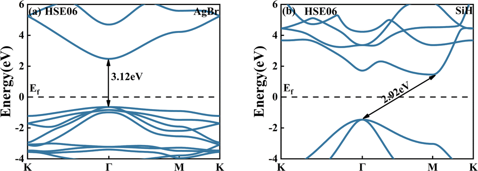
Fig. 2(a) and (b) shows the band structure of AgBr and SiH monolayers. The bandgaps for AgBr and SiH monolayers were found to be 3.12 eV and 2.92 eV respectively, which closely match the theoretical values of 3.12 eV and 2.93 eV.42,45 The AgBr monolayer exhibited a direct bandgap semiconductor behavior with its CBM and VBM located at the Γ points. Conversely, the SiH monolayer was found to be an indirect bandgap semiconductor, with its CBM situated at the M points and VBM at Γ points.
 |
| | Fig. 2 The band structures of the (a) AgBr and (b) SiH monolayers using the HSE06 functional. | |
The surface cells of the AgBr and SiH mono-layers are depicted in Fig. 3(a) and (b), respectively. Fig. 3(a) and (b) illustrates the surface cell of the AgBr and SiH monolayer. To minimize the total number of atoms and average strain in the surface cell, three configurations were chosen (see Fig. 4(a)–(f) and Table 1). These configurations are denoted as A1, A2, and A3, and they have average strains of 2.8% on the AgBr monolayer, 2.7% on the SiH monolayer, and 1.4% on both the AgBr and SiH monolayers, respectively. The average strain between these two layers falls within the 3% acceptable range, as is typical of other heterostructures, as reported before.74,75 The A1, A2, and A3 heterostructures have a hexagonal lattice structure (ϕ = 120°), with lattice constants a (b) of 7.79 Å, 7.48 Å, and 7.63 Å respectively, and each configuration consists of 28 atoms.
 |
| | Fig. 3 The surface cells of (a) AgBr and (b) SiH monolayers. The vectors v1, v2, and u1, u2 are the interface cell vectors of AgBr and SiH monolayers, respectively. ϕa and ϕb are the angles between the vectors v1, v2 and u1, u2, respectively. | |
 |
| | Fig. 4 The top views of the A1, A2, and A3 configurations are presented in (a)–(c), while their side views are shown in (d)–(f). The grey, red, blue, and brown spheres represent the Ag, Br, H, and Si atoms. | |
Table 1 The lattice constant a (b), interlayer spacing d, and binding energy Eb of the AgBr/SiH vdW heterostructures with three different arrangements, and angle ϕ between vectors
| Structure |
Strain on |
a = b (Å) |
d (Å) |
Eb (meV/atom) |
ϕ (°) |
| A1 |
AgBr (2.8%) |
7.79 |
2.45 |
−129.89 |
120 |
| A2 |
SiH (2.7%) |
7.48 |
2.35 |
−136.69 |
120 |
| A3 |
Both (1.4%) |
7.63 |
2.36 |
−134.77 |
120 |
The interlayer spacings d of the three configurations are 2.45 Å, 2.35 Å, and 2.36 Å, respectively. All of these distances are greater than what is needed for the nearest neighboring H and Br atoms in the interlayer to form a chemical bond (1.4 Å).76 These values are also larger than the interlayer spacings of 2.01 Å and 2.05 Å found in InSe/SiH and PtSe2/SiH, respectively.47,49 Moreover, the projected band structure of the three configurations show that the CBM is mainly occupied by AgBr, while the VBM is predominantly occupied by SiH, without any significant orbital hybridization (see Fig. S1(a)–(c)†). These findings demon-strate that the AgBr/SiH vdW heterostructure is a classical vdW heterostructure.
The stability of the heterostructure's struc-ture was evaluated by determining its binding energy (Eb) through the application of the formula (9). This formula calculates the energy Eb that is released when the materials are combined.77–79 A higher absolute value of binding energy indicates a greater level of stability:
| |
 | (9) |
The total energy of the AgBr/SiH vdW heter-ostructures is denoted by ETotal. Meanwhile, EAgBr and ESiH represent the total energy of the AgBr and SiH monolayers, respectively. The N signifies the total number of atoms in the heterostructure. The minor discrepancies in Eb (see Table 1) among the three configura-tions implies that all of them could be potentially found.
The Born–Oppenheimer molecular dynamics (BOMD) simulation80 was employed using a 2 × 2 × 1 supercell. The simulation was conduct-ed under the NVT Nosé–Hoover scheme at a temperature of 300 K for a duration of 10 ps. In Fig. 5(a)–(c), the total energy fluctuations of A1, A2, and A3 are 3.35 eV, 4.86 eV, and 3 eV, re-spectively, which are really small compared to the total energy of 105 magnitudes, suggesting that all three arrangements were stable at 300 K.
 |
| | Fig. 5 The time-dependent fluctuation of the total energy of (a) A1, (b) A2 and (c) A3 in AIMD simulation within 10 ps at 300 K. | |
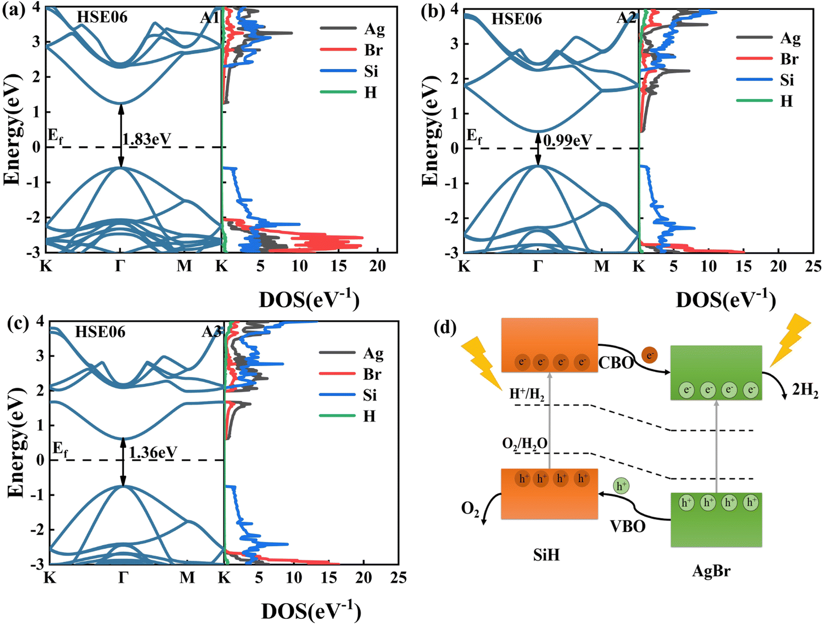
The band structures of the A1, A2, and A3 configurations are illustrated in the left panels of Fig. 6(a)–(c). These configurations possess direct bandgaps of 1.83 eV, 0.99 eV, and 1.36 eV, respectively, with their CBM and VBM located at the Γ points. It implies that the heterostructure does not necessitate the involvement of phonons for electron transitions during optical absorption. In addition, the bandgap values of the three configurations differ significantly, caused by the strain applied to the different layers.
 |
| | Fig. 6 The band structures and projected density of states (PDOS) of the (a) A1, (b) A2, and (c) A3 configurations, as calculated using the HSE06 functional, with the Fermi level denoted by horizontal black dashed lines. (d) Schematic diagram of charge transfer between AgBr/SiH vdW hetero-structure layers under solar. | |
We have also calculated the projected density of states (PDOS) of A1, A2, and A3 configurations (Fig. 6(a)–(c)). The CBMs are primarily composed of the orbitals of Ag and Br atoms, and the VBMs are mainly filled with the orbitals of Si atoms for all three configurations. Therefore, these configurations possess a type-II band alignment. When the heterostructure is irradiated with light, the conduction band offset (CBO) enables the photogenerated electrons accumulated in the CBM of SiH to be transferred to the CBM of AgBr, and the valence band offset (VBO) facilitates the movement of photogenerated holes from the VBM of AgBr to the VBM of SiH (see Fig. 6(d)). As a result, the photo-generated carriers are distributed into different layers, effectively suppressing carrier recom-bination.
To further assess their potential for photo-catalytic water splitting, we aligned the band edge positions of three configurations with the redox potential at pH levels ranging between 0 and 7, as illustrated in Fig. 7. The specific values of band edge positions relative to the vacuum energy level are summarized in Table 2. The CBMs of the A1, A2, and A3 configurations are −3.84 eV, −4.20 eV, and −4.08 eV, respectively, while VBMs of the A1, A2, and A3 configurations are −5.67 eV, −5.19 eV, and −5.44 eV, respectively. According to the formula E(H+/H2) = −4.44 eV + pH × 0.059 eV and E(O2/H2O) = −5.67 eV + pH × 0.059 eV,81 At pH = 0 (7), the potential for the reduction reaction E (H+/H2) is −4.44 eV(−4.03 eV), and the potential for the oxidation reaction (E(O2/H2O)) is −5.67 eV (−5.26 eV). Fig. 7 illustrates that the CBM and VBM of the A1 configuration can surpass the redox potential of photocatalytic water splitting at pH = 0–7, meaning that the redox reaction of photocata-lytic water splitting is feasible in the A1 configuration at pH = 0–7. Additionally, only the CBM of the A2 and A3 configurations can cross the reduction potential at pH = 0, implying that the reduction reaction of photocatalytic water splitting can occur in the A2 and A3 configurations at pH = 0. At pH = 14, all three configurations can surpass oxidation reaction potential.
 |
| | Fig. 7 The band edge positions relative to the vacuum energy level of all three configurations, along with those of AgBr and SiH monolayers at pH from 0 to 14. The purple, orange and cyan dashed lines represent the reduction potential and oxidation potential at pH = 0, 7, and 14, respectively. | |
Table 2 The bandgap (Eg) and band edge positions (ECBM and EVBM) of A1, A2, and A3 configurations relative to the vacuum energy level
| Structure |
ECBM (eV) |
EVBM (eV) |
Eg (eV) |
| A1 |
−3.84 |
−5.67 |
1.83 |
| A2 |
−4.20 |
−5.19 |
0.99 |
| A3 |
−4.08 |
−5.44 |
1.36 |
The charge differences density observed in Fig. 8(a)–(c) reveals a significant charge redistribution in the AgBr/SiH heterostructure. Specifically, there is an increase in charge near the interfacial region adjacent to the AgBr monolayer, while a decrease in charge is observed next to the SiH monolayer. This suggests a charge transfer from the hetero-structure's SiH layer to the AgBr layer. Bader charge analysis further confirms the charge transfer, with the SiH layers of A1, A2, and A3 configurations donating 0.001 |e|, 0.0111 |e|, and 0.0084 |e| to the AgBr layer, respectively. The charge transfer is similar with 0.001 |e| of PtSe2/SiH,47 0.017 |e| MoSSe/GaN,82 and 0.015 |e| WS2/GaN,83 respectively. This charge transfer can create a built-in electric field that plays a crucial role in the photoelectronic performance of the heterostructure. As shown in Fig. 9(a)–(c), the electrostatic potential drop at the two sides of the AgBr/SiH interface also indicates a significant built-in electric field from the SiH layer to the AgBr layer. Specifically, the potential drop is measured to be 2.59 eV, 5.84 eV, and 4.39 eV, respectively. These potential drop values are close to those observed in PtSe2/SiH (2.77 eV),47 MoSSe/GaN (5.23 eV),82 and WS2/GaN (6.73 eV)83 vdW heterostructures. This built-in electric field can facilitate the migration of photoelectrons from SiH to AgBr and holes from AgBr to SiH monolayer, making it a valuable feature for various photoelectronic applications. In addi-tion to the position of the band edge, the efficiency of photocatalytic water splitting is also influenced by the optical absorption coefficient, which indicates the intensity and range of optical absorption. Fig. 10 illustrates that in the UV light region, the optical absorption coefficients of A1, A2, and A3 are 4.4 × 105 cm−1, 4.2 × 105 cm−1, and 4.3 × 105 cm−1, respectively. These values represent a signifi-cant improvement compared to the isolated AgBr monolayer, which has an optical ab-sorption coefficient of 2.4 × 104 cm−1 in the UV light region. In the visible light region, the optical absorption coefficient of the A1 configuration also increased to 4 × 104 cm−1 compared to 2.2 × 104 cm−1 of isolated AgBr.
 |
| | Fig. 8 The electron difference density of the (a) A1, (b) A2, and (c) A3 configurations. The accumulation and consumption of electrons are represented by pink and cyan, respectively. | |
 |
| | Fig. 9 The electrostatic potential of the (a) A1, (b) A2, and (c) A3 configurations, respectively. | |
 |
| | Fig. 10 The optical absorption coefficient of all three configurations and the corresponding isolated monolayers. | |
Biaxial and vertical strain engineering was performed to preserve the heterostructure's original hexagonal symmetry lattice. The impact of biaxial strain on the band edges (CBMs and VBMs) of A1, A2, and A3 is depicted in Fig. 11. The CBMs shift towards higher energies while the VBMs shift towards lower energies at a biaxial tension of −5% to 5%. Specifically, in the A1 configuration, as illustrated in Fig. 11(a), the band edges can cross the redox potential of water splitting at pH = 0–7 when subjected to a biaxial tension of 0% to 5%. In the case of the A2 configuration, as shown in Fig. 11(b), the band edges can cross the redox potential at pH = 0–7 when a 5% tensile strain is applied. For the A3 configuration, as depicted in Fig. 11(c), the band edges can cross the redox potential of water splitting at pH = 0–7 when a tensile strain of more than 2% is applied. Therefore, the A1 configuration can still facilitate photocatalytic water splitting when the biaxial tensile strain is from 0% to 5%. On the other hand, when the tensile strain is 5% (2%) for the A2 (A3) configuration, it can allow photocatalytic water splitting from half-reactions (reduction reac-tion) without strain to photocatalytic overall water splitting at pH = 0–7.
 |
| | Fig. 11 The variation of the band edge positions of (a) A1, (b) A2, and (c) A3 configurations under biaxial strains −5% to 5%. The horizontal purple and orange dashed lines indicate the redox potentials at pH = 0 and 7, respectively. | |
In addition, we investigated the influence of the interlayer spacing d on the band edge position of three configurations, namely A1, A2, and A3. As demonstrated in Fig. S2,† when the interlayer spacing d is varied from 2.25 (2.26) Å to 3.25 (3.26) Å, the band gap of the A1, A2, and A3 configurations only has a minor effect on the band edge in the heterostructure. Therefore, it is likely that the alteration in interlayer spacing will have a negligible influence on the optical absorption coefficient and the photocatalytic water splitting at pH = 0–7.
We then investigated the influence of biaxial strain on the optical absorption coefficient of the heterostructure. For the A1 (A3) configurations, as shown in Fig. 12(a) and (c), the visible light region's maximum absorption coefficient increased to 5.7 × 104 cm−1 (4.6 × 104 cm−1), as the tensile strain increases to 5%. In the case of the A2 configuration, in the visible light region, as shown in Fig. 12(b), the maximum absorption coefficient increases to 2.8 × 104 cm−1 when the compressive strain of −5% is applied.
 |
| | Fig. 12 The optical absorption coefficient α of the (a) A1, (b) A2, and (c) A3 configurations under biaxial strains ranging from −5% to 5%. | |
4. Conclusion
Using DFT, we investigated the structural and optoelectronic properties of AgBr/SiH vdW heterostructures. All configurations (A1, A2, and A3) were found to be both structurally and thermodynamically stable, with direct band-gaps of 1.83 eV, 0.99 eV, and 1.36 eV, respectively, and a type-II band alignment. This alignment capitalizes on the AgBr monolayer's high electron mobility and the SiH monolayer's capacity to provide holes in heterostructures, allowing electrons to move from the SiH to the AgBr layer under the CBO, and holes to go to the SiH layer under the VBO. Our findings show that the A1, A2, and A3 configurations have optical absorption coefficients of approximately 4.0 × 10⁵ magnitude in the UV light region, which is significantly higher than the isolated AgBr monolayer's 2.4 × 104 cm−1. In the visible light region, the optical absorption coefficient of the A1 configuration also increases to 4 × 104 cm−1 than 2.2 × 104 cm−1 of isolate AgBr. The band edges of the A1 configuration are suitable for photocatalytic water splitting at pH 0–7. With a biaxial tensile strain of 5% for the A2 configuration and 2% for the A3 configuration, it can allow for photo-catalytic water splitting from half-reactions (reduction reaction) without strain to overall water splitting at pH 0–7. When the tensile strain was increased to 5%, the highest absorption coefficient for A1 and A3 configurations in the visible light region was 5.7 × 104 cm−1 and 4.6 × 104 cm−1, respectively. In light of these results, the three AgBr/SiH vdW heterostructure arrangements exhibit considerable potential for utilization in photocatalytic water splitting.
Conflicts of interest
There are no conflicts to declare.
Acknowledgements
Calculations were carried out in the High Performance Computing Laboratory of Changzhou University and by Hefei Advanced Computing Center.
References
- F. Dawood, M. Anda and G. Shafiullah, Int. J. Hydrogen Energy, 2020, 45(7), 3847–3869 CrossRef CAS.
- I. Dincer, Int. J. Hydrogen Energy, 2012, 37(2), 1954–1971 CrossRef CAS.
- S. E. Hosseini and M. A. Wahid, Int. J. Energy Res., 2020, 44(6), 4110–4131 CrossRef.
- Y. Kojima, Int. J. Hydrogen Energy, 2019, 44(33), 18179–18192 CrossRef CAS.
- K. Mazloomi and C. Gomes, Renewable Sustainable Energy Rev., 2012, 16(5), 3024–3033 CrossRef CAS.
- A. Fujishima and K. Honda, nature, 1972, 238(5358), 37–38 CrossRef CAS PubMed.
- F. E. Osterloh, Chem. Soc. Rev., 2013, 42(6), 2294–2320 RSC.
- A. Kudo and Y. Miseki, Chem. Soc. Rev., 2009, 38(1), 253–278 RSC.
- J. Tersoff, Appl. Phys. Lett., 1999, 74(15), 2122–2124 CrossRef CAS.
- X. Chen, S. Shen, L. Guo and S. S. Mao, Chem. Rev., 2010, 110(11), 6503–6570 CrossRef CAS.
- Q. Wang and K. Domen, Chem. Rev., 2019, 120(2), 919–985 CrossRef PubMed.
- K. S. Novoselov, A. K. Geim, S. V. Morozov, D.-e. Jiang, Y. Zhang, S. V. Dubonos, I. V. Grigorieva and A. A. Firsov, Science, 2004, 306(5696), 666–669 CrossRef CAS.
- L. Huang, K. Ren, H. Zhang and H. Qin, Chin. Phys. B, 2023, 32(7), 076103 CrossRef.
- W. Wu, D. Li, Y. Xu and X. C. Zeng, J. Phys. Chem. Lett., 2021, 12(47), 11488–11496 CrossRef CAS PubMed.
- Y. Xu, J. Dai and X. C. Zeng, J. Phys. Chem. Lett., 2015, 6(11), 1996–2002 CrossRef CAS PubMed.
- Y. Xu, J. Dai and X. C. Zeng, J. Phys. Chem. Lett., 2016, 7(2), 302–307 CrossRef CAS.
- Y. Xu, Q. Long, D. Li and P. Li, Phys. Chem. Chem. Phys., 2022, 24(5), 3379–3385 RSC.
- Y. Xu, Q. Long, Q. Zeng, D. Li and P. Li, J. Phys.: Condens. Matter, 2023, 35(39), 395303 CrossRef.
- A. Chaves, J. G. Azadani, H. Alsalman, D. Da Costa, R. Frisenda, A. Chaves, S. H. Song, Y. D. Kim, D. He and J. Zhou, npj 2D Mater. Appl., 2020, 4(1), 29 CrossRef CAS.
- J. Ryou, Y.-S. Kim, S. Kc and K. Cho, Sci. Rep., 2016, 6(1), 1–8 CrossRef.
- Y. Xue, Q. Zhang, W. Wang, H. Cao, Q. Yang and L. Fu, Adv. Energy Mater., 2017, 7(19), 1602684 CrossRef.
- B. Mortazavi, F. Shojaei, B. Javvaji, T. Rabczuk and X. Zhuang, Mater. Today Energy, 2021, 22, 100839 CrossRef CAS.
- V. Domnich, S. Reynaud, R. A. Haber and M. Chhowalla, J. Am. Ceram. Soc., 2011, 94(11), 3605–3628 CrossRef CAS.
- Y. Moriya, T. Takata and K. Domen, Coord. Chem. Rev., 2013, 257(13–14), 1957–1969 CrossRef CAS.
- Q.-J. Liu, Z.-T. Liu and L.-P. Feng, Phys. B, 2011, 406(3), 345–350 CrossRef CAS.
- J. Su, L. Guo, N. Bao and C. A. Grimes, Nano Lett., 2011, 11(5), 1928–1933 CrossRef CAS PubMed.
- A. C. Neto, F. Guinea, N. M. Peres, K. S. Novoselov and A. K. Geim, Rev. Mod. Phys., 2009, 81(1), 109 CrossRef.
- R. V. Gorbachev, I. Riaz, R. R. Nair, R. Jalil, L. Britnell, B. D. Belle, E. W. Hill, K. S. Novoselov, K. Watanabe and T. Taniguchi, Small, 2011, 7(4), 465–468 CrossRef CAS PubMed.
- X. Zhang, X. Xie, H. Wang, J. Zhang, B. Pan and Y. Xie, J. Am. Chem. Soc., 2013, 135(1), 18–21 CrossRef CAS.
- J. Mahmood, E. K. Lee, M. Jung, D. Shin, I.-Y. Jeon, S.-M. Jung, H.-J. Choi, J.-M. Seo, S.-Y. Bae and S.-D. Sohn, Nat. Commun., 2015, 6(1), 6486 CrossRef CAS PubMed.
- S. Singh and S. Choudhary, Opt. Quantum Electron., 2021, 53, 1–13 CrossRef.
- M. Yagmurcukardes, Y. Mogulkoc, B. Akgenç, A. Mogulkoc and F. M. Peeters, Phys. Rev. B, 2021, 104(4), 045425 CrossRef CAS.
- M. Sun, J. Liu and F. Chi, Phys. E, 2023, 145, 115467 CrossRef CAS.
- Y.-L. Hong, Z. Liu, L. Wang, T. Zhou, W. Ma, C. Xu, S. Feng, L. Chen, M.-L. Chen and D.-M. Sun, Science, 2020, 369(6504), 670–674 CrossRef CAS PubMed.
- A. K. Geim and I. V. Grigorieva, Nature, 2013, 499(7459), 419–425 CrossRef CAS PubMed.
- A. Castellanos-Gomez, X. Duan, Z. Fei, H. R. Gutierrez, Y. Huang, X. Huang, J. Quereda, Q. Qian, E. Sutter and P. Sutter, Nat. Rev. Methods Primers, 2022, 2(1), 58 CrossRef CAS.
- Y. Liu, N. O. Weiss, X. Duan, H.-C. Cheng, Y. Huang and X. Duan, Nat. Rev. Mater., 2016, 1(9), 1–17 Search PubMed.
- C. Zhang, J. Xu, H. Song, K. Ren, Z. G. Yu and Y.-W. Zhang, Molecules, 2023, 28(11), 4334 CrossRef CAS PubMed.
- F. Opoku, S. O.-B. Oppong, A. Aniagyei, O. Akoto and A. A. Adimado, RSC Adv., 2022, 12(12), 7391–7402 RSC.
- H. Qiao, Y. Zhang, Z.-H. Yan, L. Duan, J.-B. Fan and L. Ni, Surf. Sci., 2022, 723, 122103 CrossRef CAS.
- J. Zhou, L. Shen, M. D. Costa, K. A. Persson, S. P. Ong, P. Huck, Y. Lu, X. Ma, Y. Chen and H. Tang, Sci. Data, 2019, 6(1), 86 CrossRef PubMed.
- X. Huang, L. Yan, Y. Zhou, Y. Wang, H.-Z. Song and L. Zhou, J. Phys. Chem. Lett., 2020, 12(1), 525–531 CrossRef PubMed.
- W. Wang, S. Dai, X. Li, J. Yang, D. J. Srolovitz and Q. Zheng, Nat. Commun., 2015, 6(1), 7853 CrossRef CAS PubMed.
- A. F. Wani, B. Rani, S. Dhiman, U. B. Sharopov and K. Kaur, Int. J. Energy Res., 2022, 46(8), 10885–10893 CrossRef CAS.
- J. Zeng, L. Xu, X. Luo, B. Peng, Z. Ma, L.-L. Wang, Y. Yang and C. Shuai, Phys. Chem. Chem. Phys., 2021, 23(4), 2812–2818 RSC.
- M. Niu, D. Cheng and D. Cao, Sci. Rep., 2014, 4(1), 4810 CrossRef CAS PubMed.
- S. Han, Y. Li and Z. Wang, Phys. Chem. Chem. Phys., 2020, 22(30), 17145–17151 RSC.
- F. Opoku, A. Aniagyei, O. Akoto, E. E. Kwaansa-Ansah, N. K. Asare-Donkor and A. A. Adimado, Mater. Adv., 2022, 3(11), 4629–4640 RSC.
- W. Sheng, Y. Xu, M. Liu, G. Nie, J. Wang and S. Gong, Phys. Chem. Chem. Phys., 2020, 22(37), 21436–21444 RSC.
- L. Lv, X. Ma, W. Lou, X. Zhang, C. Shen, C. Xia and Y. Liu, Phys. Status Solidi B, 2022, 259(7), 2100666 CrossRef CAS.
- S. Han, Y. Li and Z. Wang, Phys. E, 2021, 134, 114869 CrossRef CAS.
- H.-F. Lin, H.-Y. Liu, M. Wang, S.-S. Wang, T.-P. Hou and K.-M. Wu, Phys. Chem. Chem. Phys., 2022, 24(7), 4425–4436 RSC.
- S. Feng, F. Guo, C. Yuan, Z. Wang, F. Miao and H. Zhang, Mater. Adv., 2022, 3(24), 9063–9070 RSC.
- R. Frisenda, M. Drüppel, R. Schmidt, S. Michaelis de Vasconcellos, D. Perez de Lara, R. Bratschitsch, M. Rohlfing and A. Castellanos-Gomez, npj 2D Mater. Appl., 2017, 1(1), 10 CrossRef.
- A. Michail, D. Anestopoulos, N. Delikoukos, J. Parthenios, S. Grammatikopoulos, S. A. Tsirkas, N. N. Lathiotakis, O. Frank, K. Filintoglou and K. Papagelis, 2D Materials, 2020, 8(1), 015023 CrossRef.
- N. Ferdous, M. S. Islam, J. Biney, C. Stampfl and J. Park, Sci. Rep., 2022, 12(1), 20106 CrossRef CAS.
- J. Ye, J. Liu and Y. An, Appl. Surf. Sci., 2020, 501, 144262 CrossRef CAS.
- X. Yuan, Y. Guo, J. Wang, G. Hu, J. Ren and X. Zhao, Front. Chem., 2022, 10, 155 Search PubMed.
- H. Wang, B. Zhou and W. Li, Phys. Chem. Chem. Phys., 2023, 25(1), 486–493 RSC.
- S. Feng, J. Liu, J. Chen, L. Su, F. Guo, C. Tang, C. Yuan and X. Cheng, Appl. Surf. Sci., 2022, 604, 154620 CrossRef CAS.
- P. Geerlings, F. De Proft and W. Langenaeker, Chem. Rev., 2003, 103(5), 1793–1874 CrossRef CAS.
- A. J. Cohen, P. Mori-Sánchez and W. Yang, Chem. Rev., 2012, 112(1), 289–320 CrossRef CAS.
- S. Smidstrup, T. Markussen, P. Vancraeyveld, J. Wellendorff, J. Schneider, T. Gunst, B. Verstichel, D. Stradi, P. A. Khomyakov and U. G. Vej-Hansen, J. Phys.: Condens. Matter, 2019, 32(1), 015901 CrossRef PubMed.
- S. Smidstrup, D. Stradi, J. Wellendorff, P. A. Khomyakov, U. G. Vej-Hansen, M.-E. Lee, T. Ghosh, E. Jónsson, H. Jónsson and K. Stokbro, Phys. Rev. B, 2017, 96(19), 195309 CrossRef.
- S. Grimme, J. Comput. Chem., 2006, 27(15), 1787–1799 CrossRef CAS PubMed.
- Y. Xu, J. Han, Z. Li and Z. Zhang, J. Phys. D: Appl. Phys., 2023, 56(36), 365504 CrossRef.
- J. Heyd, G. E. Scuseria and M. Ernzerhof, J. Chem. Phys., 2003, 118(18), 8207–8215 CrossRef CAS.
- L. Jelver, P. M. Larsen, D. Stradi, K. Stokbro and K. W. Jacobsen, Phys. Rev. B, 2017, 96(8), 085306 CrossRef.
- S. Deng, Y. Zhang and L. Li, Appl. Surf. Sci., 2019, 476, 308–316 CrossRef CAS.
- S. Deng, L. Li and P. Rees, ACS Appl. Nano Mater., 2019, 2(6), 3977–3988 CrossRef CAS.
- R. M. Martin, Electronic structure: basic theory and practical methods, Cambridge university press, 2020 Search PubMed.
- D. J. Griffiths, Am. J. Phys., 2005, 73(6), 574 CrossRef.
- O. D. Restrepo, R. Mishra, J. E. Goldberger and W. Windl, J. Appl. Phys., 2014, 115(3), 033711 CrossRef.
- Y. Matsushita, H. Nishi, J. Iwata, T. Kosugi and A. Oshiyama, Phys. Rev. Mater., 2018, 2(1), 010801 CrossRef CAS.
- Z. Wang, Q. Chen and J. Wang, J. Phys. Chem. C, 2015, 119(9), 4752–4758 CrossRef CAS.
- N. L. Pivonka, C. Kaposta, G. von Helden, G. Meijer, L. Wöste, D. M. Neumark and K. R. Asmis, J. Chem. Phys., 2002, 117(14), 6493–6499 CrossRef CAS.
- S. Jing, J. Pan, W. Chen, W. Li, B. Bian, B. Liao and G. Wang, Comput. Mater. Sci., 2022, 210, 111463 CrossRef CAS.
- X. Jiang, Q. Gao, X. Xu, G. Xu, D. Li, B. Cui, D. Liu and F. Qu, Phys. Chem. Chem. Phys., 2021, 23(38), 21641–21651 RSC.
- K. Lazaar, M. Barhoumi and M. Said, Comput. Mater. Sci., 2022, 201, 110912 CrossRef CAS.
- M. Born, J. Oppenheimer, B. Sutcliffe and W. Geppert, Ann. Phys., 1927, 84, 457 CrossRef CAS.
- L. Xu, Y. Zhang, Z. Ma, T. Chen, C. Guo, C. Wu, H. Li, X. Huang, S. Tang and L.-L. Wang, Int. J. Hydrogen Energy, 2023, 48(48), 18301–18314 CrossRef CAS.
- M. Idrees, C. V. Nguyen, H. Bui, I. Ahmad and B. Amin, Phys. Chem. Chem. Phys., 2020, 22(36), 20704–20711 RSC.
- H. Shu, Mater. Sci. Eng. B, 2020, 261, 114672 CrossRef CAS.
Footnote |
| † Electronic supplementary information (ESI) available: the projected band structure of (a) A1, (b) A2, and (c) A3 configurations (Fig. S1); the band edge positions of (a) A1, (b) A2, and (c) A3 configurations with changing interlayer spacing d go from 2.25 (2.26) Å to 3.25 (3.26) Å in the pH range of 0 to 7 (Fig. S2). See DOI: https://doi.org/10.1039/d3ra05079c |
|
| This journal is © The Royal Society of Chemistry 2023 |
Click here to see how this site uses Cookies. View our privacy policy here. 
 Open Access Article
 This Open Access Article is licensed under a Creative Commons Attribution-Non Commercial 3.0 Unported Licence
 *a,
Dongze Lia,
Qiang Zenga,
He Suna and
Pengfei Lib
*a,
Dongze Lia,
Qiang Zenga,
He Suna and
Pengfei Lib