DOI:
10.1039/D3RA04503J
(Paper)
RSC Adv., 2023,
13, 33062-33066
Carbon nanotube papers with p–n junctions along the thickness direction†
Received
6th July 2023
, Accepted 3rd November 2023
First published on 9th November 2023
Abstract
Conductive papers made from carbon nanotubes and wood fibers exhibit a p-type character. N2 plasma treatment converts paper into n-type and conversion is verified by elemental analyses, work function and Hall-effect measurements. By screening one face of p-type paper in plasma, the p–n junctions are successfully created along the thickness direction and electrical rectification is evident by current–voltage measurement.
1 Introduction
Diodes are two-terminal electronic devices made of different semiconductor materials (e.g. p–n junction).1,2 Accordingly, a built-in-potential (ΔE) forms at the interface where bands bend and Fermi levels (EF) equalize. This junction barrier, also known as the depletion layer (DL), becomes thinned in forward bias thus allowing current to flow. Application of reverse bias, in contrast, widens the DL so current cannot pass until breakdown.3 Electrical rectification is also present in hetero-junction nanowires and doped nanostructures; the former is produced through catalytic pyrolysis of hydrocarbons and is verified to be Schottky type.4 The latter is of p–n type where the DL is made by coating of polymers onto carbon nanotubes (CNTs).5
CNTs are one-dimensional conductors made of rounded graphite sheets and can be made in a large quantity through different means.5 The electronic properties of CNTs are peculiar in that the band structure is determined by tube diameter (d) and chirality (θ) expressed as d = (3)1/2 × ac–c (m2 + mn + n2)1/2/π and θ = tan−1[31/2 × m/(2n + m)] where ac–c, n and m are C–C bond length (=1.42 Å) and integers. For a given (n, m), metallic tubes satisfy 2n + m = 3q (q: integer) and 2n + m ≠ 3q for semiconducting CNTs with the band gap approximating Eg = φ × ac–c/d (φ = 3 eV).6 However, creation of electronic devices on individual CNTs remains unfavourable thus far; first, current techniques cannot make CNTs with similar d and θ so band structure appears to vary from tube to tube;7 second, CNTs either made by catalytic pyrolysis of hydrocarbons or electrical arc discharge of graphite do not have all sp2 valencies satisfied so electronic properties are actually governed by localized states around band edges, e.g. functionalized and doped lattices.8–10 In this work, we demonstrate the production of CNT papers with p–n junctions along the thickness direction where ΔE is created by N2 plasma. Papers are flexible and can be scaled up to cm2 dimension for practical use, e.g. voltage doubling and output smoothing.3
2 Experimental
2.1. Production of p-type CNTs conductive paper
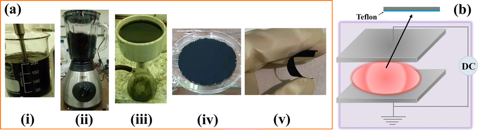
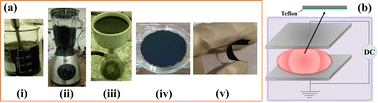
As-made CNTs behave as p-type in air and are therefore used as starting materials (multi-walled, 8–35 μm in length, 3–40 nm in diameter, 85–95% purity, Conjutek, Taiwan).11 However, bulk CNTs are in powder form and cannot firmly bind together without plastic binders. In order to avoid use of plastics the CNTs are mixed with wood fibres (WFs, i.e. plant-based tissue paper with CaCO3 < 5 wt%).12 First, CNTs are ultrasonically dispersed in deionized water (200 ml) and suspension is poured into a blender (rpm = 1500 and power = 1200 W, i → ii, Fig. 1a). Second, tissue paper is added into CNT suspension and the mixture is stirred for 10 min, followed by filtering in a vacuum-suction system and hot-pressing (50 kg cm−2, 30 min) to form flexible CNTs-WF papers hereafter defined as p-CNT-WF (iii–v, Fig. 1a). Paper dimension is 150 × 150 × 0.3 mm and the filling fraction (fCNT) of CNTs in WF is set at 1, 10, 20, 30 and 40 wt%.
 |
| | Fig. 1 Production of p-CNT-WF (a) and creation of p–n junctions across p-CNT-WF by N2 plasma treatments (b). Teflon coverage is denoted by arrow. | |
2.2. Production of B-doped CNTs conductive paper
Conductive papers are also made from boron-doped multi-walled CNTs (B-CNTs) known as an enhanced p-type with hole carrier density 5–6 times greater than un-doped.13 First, B2O3 powder (2 g) and CNTs (6 g) are ultrasonically mixed in deionized water (200 ml) and suspension is dried in an oven (60 °C). Second, the mixture is heated to 1200 °C in Ar flow (100 sccm) for 4 h, followed by methanol (100 ml, 1 h) rinsing to remove residual oxides (i.e. 2B2O3 + 15C → 4BC3 + 3CO2).14 Third, B-CNT-WF is made according to same procedures described in Fig. 1a.
2.3. Creation of p–n junctions across p-CNT-WF thickness
The non-thermal equilibrium plasma operates at room temperature and is widely used for a variety of chemical purposes, e.g. surface cleaning and modification.15,16 The N2 plasma is used to create p–n junctions across the p-CNT-WF thickness according to following procedures. First, one face of a p-CNT-WF is covered with Teflon film (Fig. 1b). Second, one-face screened paper is subjected to N2 plasma at 0.3 torr and 180 V for 10–20 min. Plasma treated papers are hereafter defined as p-CNT-WF/n-CNT-WF(t) where slash denotes interface between Teflon protected (i.e. p-CNT-WF) and plasma treated faces (n-CNT-WF) and, the subscript t denotes plasma treating time. Similar procedures are also applied to B-CNT-WF and resultant papers are defined as B-CNT-WF/n-CNT-WF(t).
2.4. Electrical resistivity measurements of p-CNT-WF
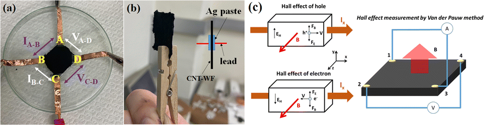
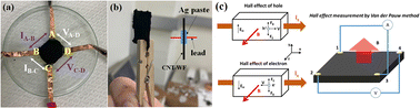
Electrical resistivity (ρ) of p-CNT-WF is measured by van der Pauw technique (i.e. four-terminal method) which excludes contact resistance and determines paper resistance (R) according to equation e(−πaR1/ρ) + e(−πaR2/ρ) = 1 where R1 = VDC/IAB, R2 = VAD/IBC and a is paper thickness (=0.3 mm, Fig. 2a).17 Measurements are carried out on papers made of different fCNT so the electrical percolation threshold (η) and optimal fCNT for making p–n junctions can be determined.
 |
| | Fig. 2 Four-terminal measurements for p-CNT-WF made of different fCNT (a) and two-terminal measurements for p-CNT-WF/n-CNT-WF and B-CNT-WF/n-CNT-WF (b). Schematic diagram of Hall effect (left) and the Hall effect measurement by van der Pauw method (right, c). | |
2.5. Two-terminal measurements of p-CNT-WF/n-CNT-WF(t) and B-CNT-WF/n-CNT-WF(t)
The I–V characters of p-CNT-WF/n-CNT-WF and B-CNT-WF/n-CNT-WF are studied by two-terminal DC technique (Keithley, Source meter 2450 & Agilent B1500A). First, two electrical leads are glued to both faces of p-CNT-WF/n-CNT-WF respectively using conductive Ag paste (Fig. 2b). Second, the forward and reverse bias measurements are carried out at ±5 V to determine threshold voltage (Vth), maximum forward current (IF) and ratio of reverse to forward resistance (RR/RF) where RR/RF ≈ 1 for ohmic conductor (i.e. symmetric I–V profile) and RR/RF > 1 for polarized conductors.3 Third, all measurements are performed in a chamber with relative humidity and temperature controlled at 25–30% and 25 °C to evade water doping.18
2.6. Structural characterization, Raman and elemental analyses of p-, B- and n-CNT-WF(t)
CNT papers are inspected by scan electron microscope (SEM, Hitachi-SU8010) which gives information regarding to surface texture and CNT distribution. Raman is a powerful tool widely used to characterize carbon structures based on D and G-bands; the former appears as a result of phonon scattering at zone boundaries (A1g mode = 1375 cm−1) and becomes strong as defect density increases. The latter comes from C–C bond stretching (E2g mode = 1583 cm−1) and is present in all sp2 bonded structures. Accordingly, the degree of graphitization can be characterized by ID/IG where ID and IG represent intensity of D and G-bands.19 In this work, Raman spectra of CNTs papers are recorded by Horiba-HR800 at room temperature and bonding characters are analysed using X-ray photoelectron emission spectroscopy (XPS, ULVAC-PHI PHI 5000 Versaprobe II); the XPS peak intensity is calculated according to the full width at half maximum and elemental ratio (Qx) of C 1s, O 1s, N 1s and B 1s spectra expressed as Qx = nx/Σni = (Sx/Xx)/Σ(Si/Xi) where Xx is corrected relative sensitivity factor and Sx is signal intensity.20
2.7. Work function and Hall effect measurements of p-, B- and n-CNT-WF(t)
The work function (Φ) of CNT papers is calculated according to equation Φ = hv − Eo − EF where excitation energy (hv), secondary electron cut-off energy (Eo) and the Fermi energy (EF) are determined by tangential equation and ultraviolet photoelectron spectroscopy (UPS) at hv = 21.22 eV. The Φ and UPS are only calculated and recorded for samples made with p-CNT-WF, n-CNT-WF and B-CNT-WF (ESI 1†). Carrier concentration of CNT papers is probed by Hall-effect measurement system using 80–350 K and 15 × 15 mm sample kit (Ecopia, HMS 5000). Fig. 2c shows working principe (left) and setup of Hall effect measurement (right) based on the van der Pauw method where Hall voltage (VH) and Hall coefficient (RH) are expressed as VH = VA + VB + VC + VD (Fig. 2a) and RH = VHa/IxB (a, B and Ix denote sample thickness, magnetic field and current in x direction).
3 Results and discussion
Fig. 3a shows a SEM image of p-CNT-WF, along with the ρ–fCNT plot (insert). Clearly, the WF structure is of band-like and ranges at 5–30 μm in width and 0.7–1.2 mm in length (ESI 2†). It is worth mentioning that papers made of pure CNTs lack sustainable strength and dissociate rapidly with stressing (e.g. handling and sampling). Addition of WFs into CNTs truly improves paper strength, as evident by stress–strain curve where tensile strength reaches 15.8 MPa; a value which is comparable with oxides based flexible devices (ESI 3†).10 Four-terminal measurements and SEM images verify the p-CNT-WF to be electrically conductive with η–fCNT = 20 wt%; (i) ρ decreases rapidly at fCNT = 10–20 wt% (insert, Fig. 3a); (ii) CNTs network on WFs (circles 1 and 2, Fig. 3b and c). Accordingly, all characterizations are carried out on conductive papers made of fCNT = 20 wt%. Electrical measurements carried out along in-plane and out-of-plane directions of p-CNT-WF confirm the ρ difference to be as low as 0.05 Ω m (ESI 4†). SEM images however fail to identify structural alternation of CNTs before and after plasma treatments (ESI 5†).
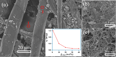 |
| | Fig. 3 SEM image of p-CNT-WF. Insert: the ρ–fCNT plot of p-CNT-WF (a). Enhanced SEM images of circles 1 and 2 (b and c). | |
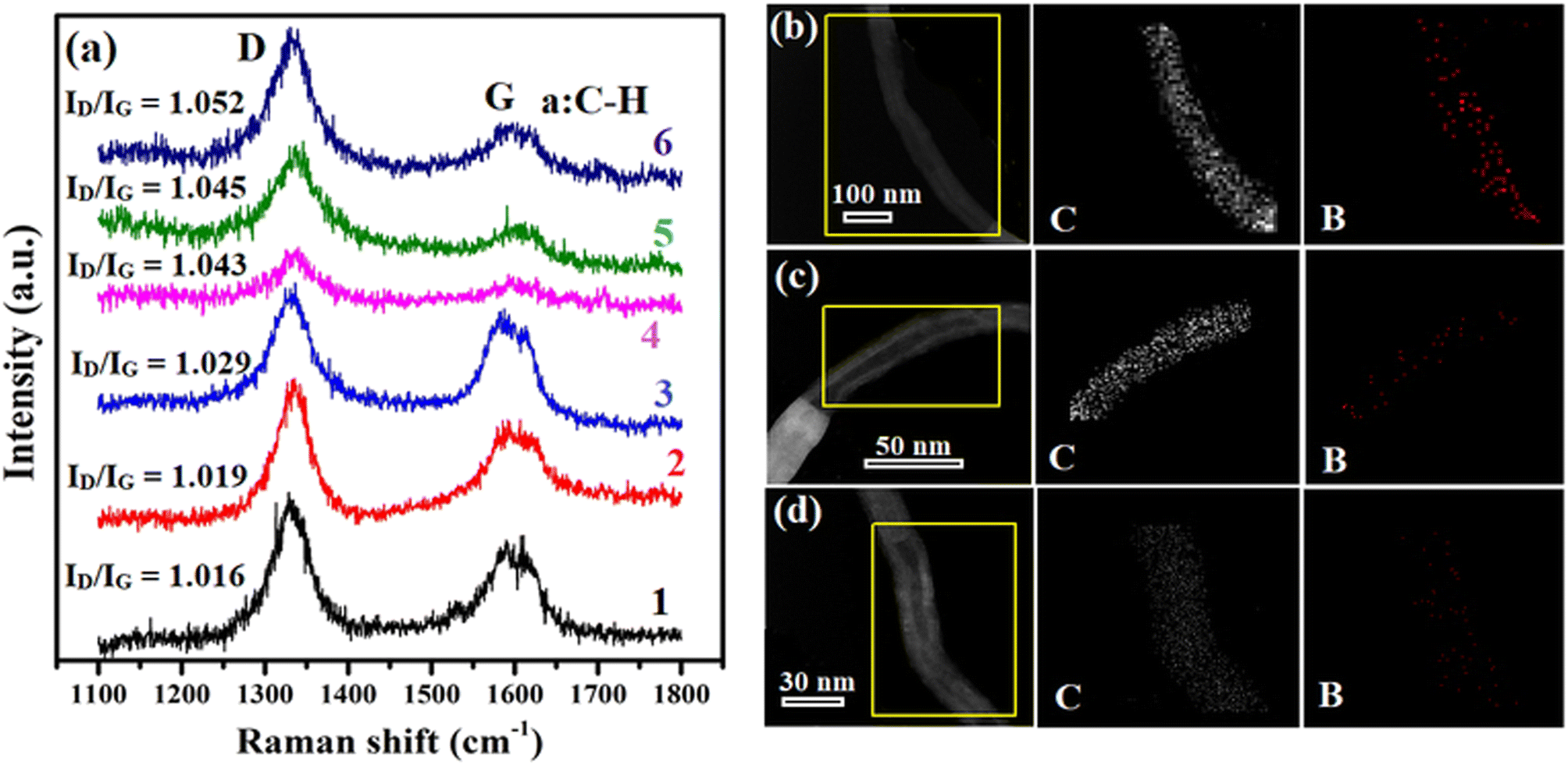
Fig. 4a shows Raman spectra and calculated ID/IG where hydrogenated amorphous carbon often seen in pyrolysis made CNTs is also present (a: C–H = 1587 cm−1).19 Clearly, the ID/IG increases with plasma treatments, indicative of surface modification enhanced A1g mode.19 Table 1 lists content of O 1s, C 1s, N 1s and B 1s according to deconvoluted XPS spectra where bonding characters are identified to be C![[double bond, length as m-dash]](https://www.rsc.org/images/entities/char_e001.gif) C (284.7 eV), CO (531.2 eV), C–O (532.4 eV), O–CO (533.4 eV), graphitic-N (NQ, 401 eV), pyridinic-N (N6, 398.3 eV), B–N (190.6 eV), C–B (191.2 eV) and B–O (192.2 eV) (ESI 6–8†).
C (284.7 eV), CO (531.2 eV), C–O (532.4 eV), O–CO (533.4 eV), graphitic-N (NQ, 401 eV), pyridinic-N (N6, 398.3 eV), B–N (190.6 eV), C–B (191.2 eV) and B–O (192.2 eV) (ESI 6–8†).
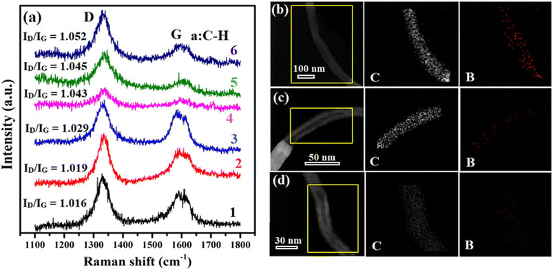 |
| | Fig. 4 Raman spectra and ID/IG of all samples where curve 1–6 stands for p-CNT-WF, n-CNT-WF(10min), n-CNT-WF(20min), B-CNT-WF, B-CNT-WF(10min) and B-CNT-WF(20min) (a). The C and B mapping on individual B-CNTs (b–d). | |
Table 1 Elemental content of all samples studied
| Samples |
Elements (at%) |
| O |
C |
N |
B |
| p-CNT-WF |
32.94 |
66.61 |
0.41 |
0.05 |
| n-CNT-WF(10min) |
34.36 |
63.14 |
2.43 |
0.07 |
| n-CNT-WF(20min) |
34.98 |
61.97 |
2.98 |
0.06 |
| B-CNT-WF |
40.51 |
56.97 |
0.72 |
1.8 |
| B-CNT-WF(10min) |
35.19 |
61.63 |
1.82 |
1.36 |
| B-CNT-WF(20min) |
39.95 |
55.35 |
2.77 |
1.92 |
First, the O 1s content increases while C 1s decreasing, indicative of oxygenation through reactions of absorbed O2 with carbon lattices (i.e. conversion of CC into C–O, CO and O–CO).20 Second, N2 plasma induced nitridation is evident by increased N 1s content in n-CNT-WF(10min) and n-CNT-WF(20min). Third, conversion of p-CNT-WF into B-CNT-WF is supported by (i) B–C bond formation (191.2 eV) and increased B 1s content (ESI 8†); (ii) C 1s and B 1s mapping analyses (Fig. 4b–d); (iii) B–N bond formations (190.6 eV, ESI 8†). Additional evidence in support of p → n conversion comes from Φ and Hall-effect measurements; the former shows a decrease by 15–16% and is attributed to electronegativity from lone pairs of O and N (Table 2).
Table 2 Φ and carrier concentration/mobility of samples studied
| Samples |
Φ (eV) |
Carrier con. (cm−2) |
Mobility (cm2 V−1 s−1) |
| p-CNT-WF |
4.62 |
5.642 × 10¹³ |
1303.3 |
| n-CNT-WF(10min) |
3.86 |
−2.47 × 10¹³ |
2691.9 |
| n-CNT-WF(20min) |
3.92 |
−5.92 × 10¹³ |
1099.7 |
| B-CNT-WF |
5.22 |
9.8 × 10¹³ |
797.2 |
The latter displays a transition from hole- to electron-governed carriers, indicative of both O and N acting as n-dopants. It is worth mentioning for an electron–hole symmetric semiconductor that EF lies at the middle of Eg between valence (VB) and conduction band edge (CB). Doping, however, creates localized states near to band edge, for example, n-/p-doped states appear in the vicinity of CB/VB edge. In this case, the localized states become the new edge and EF needs to be redefined.8
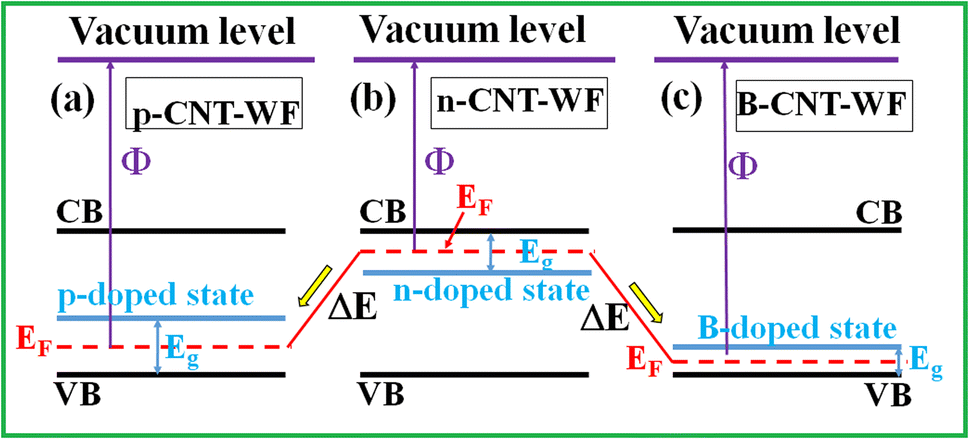
Fig. 5a shows band diagram of p-CNT-WF where EF lies at the middle of Eg between VB and p-doped state arising from electron-deficient defects.8 N2 plasma creates n-doped state near to the CB so EF is lifted and a ΔE forms between p- and n-CNT-WF(t) (Fig. 5a and b). B-Doping enhances p-type character and moves p-doped state much closer to VB so Φ increases and ΔE becomes greater (Fig. 5b and c & Table 2). It is worth mentioning that carrier concentration and mobility uncovered here are consistent with reported data on CNTs (Table 2).8
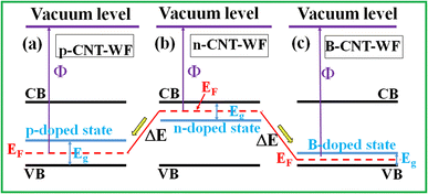 |
| | Fig. 5 Band diagrams of p-CNT-WF (a), n-CNT-WF (b) and B-CNT-WF (c); yellow arrows indicate forward bias direction. | |
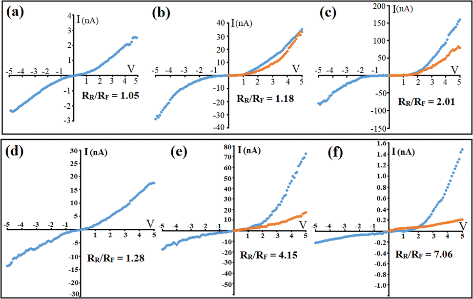
Since diodes are unidirectional conductors, the p- and n-sides of p-CNT-WF/p-CNT-WF, p-CNT-WF/n-CNT-WF(t) and B-CNT-WF/n-CNT-WF(t), made of fCNT = 20 wt% (insert, Fig. 3a), are connected to positive and negative electrodes of a power supply (i.e. the forward bias direction, yellow arrows, Fig. 5). Fig. 6 displays I–V curves of p-CNT-WF/p-CNT-WF (a), p-CNT-WF/n-CNT-WF(10min) (b) and p-CNT-WF/n-CNT-WF(20min) (c) where profiles recorded at the 3rd (i.e. negative region) are also superimposed on the 1st quadrant to highlight diode character (i.e. positive region and orange). Clearly, a symmetric I–V curve is present in p-CNT-WF/p-CNT-WF with RR/RF = 1.05, indicative of an ohmic conductor (Fig. 6a). Asymmetric profiles however are present in p-CNT-WF/n-CNT-WF(10min) and p-CNT-WF/n-CNT-WF(20min); the latter resembles a diode and the RR/RF, IF and Vth are measured to be 2.01, 165 nA and 1.9 V. This value is lower than that of Si based (IF = 10−3–10−5 A and Vth = 0.5–0.7) and is due to fact that conductive papers are made from a large number of CNTs connected in parallel, i.e. Vth = V1 = V2 = V3 & IF = I1 + I2 + I3… where Vn and In denote V and I contribution by individual tubes.21,22 A similar trend is also observed in B-CNT-WF/B-CNT-WF and B-CNT-WF/n-CNT-WF(10min) with RR/RF = 1.28 and 4.15; the latter again verifies B-doping enhanced p-character (Fig. 6d and e). Surprisingly, the RR/RF reaches 7.06 for B-CNT-WF/n-CNT-WF(20min) (Fig. 6f); a value which is comparable with conventional Si-based devices and is consistent with Fig. 5 & Table 2. Abbreviation in manuscript are list in Table 3.
 |
| | Fig. 6 I–V profiles of p-CNT-WF/p-CNT-WF (a), p-CNT-WF/n-CNT-WF(10min) (b), p-CNT-WF/n-CNT-WF(20min) (c), B-CNT-WF/B-CNT-WF (d), B-CNT-WF/n-CNT-WF(10min) (e) and B-CNT-WF/n-CNT-WF(20min) (f); all samples are made of fCNT = 20 wt%. | |
Table 3 Abbreviation list
| Abbreviation |
Full name |
| ΔE |
Built-in-potential |
| EF |
Fermi levels |
| DL |
Depletion layer |
| d |
Tube diameter |
| θ |
Tube chirality |
| ac–c |
C–C bond length |
| Eg |
Band gap |
| fCNT |
Filling fraction |
| WFs |
Wood fibres |
| ρ |
Electrical resistivity |
| a |
Paper thickness |
| η |
Electrical percolation threshold |
| Vth |
Threshold voltage |
| IF |
Maximum forward current |
| RR |
Reverse resistance |
| RF |
Forward resistance |
| ID |
Intensity of D band |
| IG |
Intensity of G band |
| Qx |
Elemental ratio |
| Xx |
Corrected relative sensitivity factor |
| Sx |
Signal intensity |
| Φ |
Work function |
| hv |
Excitation energy |
| VH |
Hall voltage |
| RH |
Hall coefficient |
| Ix |
Current in x direction |
| B |
Magnetic field |
| VB |
Valence band |
| CB |
Conduction band |
4 Conclusions
Flexible conductive papers are made from CNTs and WFs. As-made papers behave as p-type and can be changed into n-type through N2 plasma treatments. Elemental analyses confirm formation of graphitic N structure after N2 plasma treatments thus reducing ϕ from 4.62 to 3.86 eV. The B-doping enhances p-type character so ϕ increases to 5.22 eV. By screening one face of p-CNT-WF in plasma, p–n junctions are successfully created along paper thickness direction and are verified by electrical rectification and RR/RF ≫ 1. The RR/RF of B-CNT-WF/n-CNT-WF(20min) reaches a value as high as 7.06.
Conflicts of interest
The authors declare no conflict of interest.
Acknowledgements
Authors thank the National Science and Technology Council (NSTC) of Taiwan for the financial support (MOST-110-2112-M-007-014). Authors also acknowledge the use of F200 HRTEM and ARM200 Cs TEM which belong to Instrumentation Centre at National Tsing-Hua University (NTHU) under funding by the National Science and Technology Council (NSTC) of Taiwan.
References
- B. D. Gates, Flexible Electronics, Science, 2009, 323, 1566–1567 CrossRef CAS PubMed.
- Y. G. Gurevich and G. N. Logvinov, Physics of thermoelectric cooling, Semicond. Sci. Technol., 2005, 20, R57 CrossRef CAS.
- P. R. Wilson, Measurements on the depletion layer properties of planar diodes, Solid-State Electron., 1969, 12, 539–547 CrossRef.
- J. Hu, M. Ouyang, P. Yang and C. M. Lieber, Controlled growth and electrical properties of heterojunctions of carbon nanotubes and silicon nanowires, Natur, 1999, 399, 48–51 CrossRef CAS.
- C. Zhou, J. Kong, E. Yenilmez and H. Dai, Modulated Chemical Doping of Individual Carbon Nanotubes, Science, 2000, 290, 1552–1555 CrossRef CAS PubMed.
- M. S. Dresselhaus, G. Dresselhaus and A. Jorio, UNUSUAL PROPERTIES AND STRUCTURE OF CARBON NANOTUBES, Annu. Rev. Mater. Res., 2004, 34, 247–278 CrossRef CAS.
- T. W. Ebbesen, H. J. Lezec, H. Hiura, J. W. Bennett, H. F. Ghaemi and T. Thio, Electrical conductivity of individual carbon nanotubes, Natur, 1996, 382, 54–56 CrossRef CAS.
- K. Liu, P. Avouris, R. Martel and W. K. Hsu, Electrical transport in doped multiwalled carbon nanotubes, Phys. Rev. B: Condens. Matter Mater. Phys., 2001, 63, 161404 CrossRef.
- J. B. Bult, R. Crisp, C. L. Perkins and J. L. Blackburn, Role of Dopants in Long-Range Charge Carrier Transport for p-Type and n-Type Graphene Transparent Conducting Thin Films, ACS Nano, 2013, 7, 7251–7261 CrossRef CAS PubMed.
- J. E. Cha, S. Y. Kim and S. H. Lee, Effect of Continuous Multi-Walled Carbon Nanotubes on Thermal and Mechanical Properties of Flexible Composite Film, Nanomaterials, 2016, 6, 182 CrossRef PubMed.
- P. G. Collins, K. Bradley, M. Ishigami and A. Zettl, Extreme Oxygen Sensitivity of Electronic Properties of Carbon Nanotubes, Science, 2000, 287, 1801–1804 CrossRef CAS PubMed.
- S. Durukan and F. Karadagli, Physical characteristics, fiber compositions, and tensile properties of nonwoven wipes and toilet papers in relevance to what is flushable, Sci. Total Environ., 2019, 697, 134135 CrossRef PubMed.
- W. K. Hsu, S. Y. Chu, E. Muñoz-Picone, J. L. Boldú, S. Firth, P. Franchi, B. P. Roberts, A. Schilder, H. Terrones, N. Grobert, Y. Q. Zhu, M. Terrones, M. E. McHenry, H. W. Kroto and D. R. M. Walton, Metallic behaviour of boron-containing carbon nanotubes, Chem. Phys. Lett., 2000, 323, 572–579 CrossRef CAS.
- W. Han, Y. Bando, K. Kurashima and T. Sato, Boron-doped carbon nanotubes prepared through a substitution reaction, Chem. Phys. Lett., 1999, 299, 368–373 CrossRef CAS.
- J.-J. Zeng and Y.-J. Lin, Tuning the work function of graphene by nitrogen plasma treatment with different radio-frequency powers, Appl. Phys. Lett., 2014, 104, 233103 CrossRef.
- J. Duch, P. Kubisiak, K. H. Adolfsson, M. Hakkarainen, M. Golda-Cepa and A. Kotarba, Work function modifications of graphite surface via oxygen plasma treatment, Appl. Surf. Sci., 2017, 419, 439–446 CrossRef CAS.
- D. W. Koon and C. J. Knickerbocker, What do you measure when you measure resistivity?, Rev. Sci. Instrum., 1992, 63, 207–210 CrossRef.
- P. S. Na, H. Kim, H.-M. So, K.-J. Kong, H. Chang, B. H. Ryu, Y. Choi, J.-O. Lee, B.-K. Kim, J.-J. Kim and J. Kim, Investigation of the humidity effect on the electrical properties of single-walled carbon nanotube transistors, Appl. Phys. Lett., 2005, 87, 093101 CrossRef.
- M. S. Dresselhaus, G. Dresselhaus, R. Saito and A. Jorio, Raman spectroscopy of carbon nanotubes, Phys. Rep., 2005, 409, 47–99 CrossRef.
- J.-L. Li, K. N. Kudin, M. J. McAllister, R. K. Prud’homme, I. A. Aksay and R. Car, Oxygen-Driven Unzipping of Graphitic Materials, Phys. Rev. Lett., 2006, 96, 176101 CrossRef PubMed.
- J. P. McKelvey, Solid state and semiconductor physics, Harper & Row, 2018 Search PubMed.
- P. C. P. Watts, W.-K. Hsu, H. W. Kroto and D. R. M. Walton, Are Bulk Defective Carbon Nanotubes Less Electrically Conducting?, Nano Lett., 2003, 3, 549–553 CrossRef CAS.
|
| This journal is © The Royal Society of Chemistry 2023 |
Click here to see how this site uses Cookies. View our privacy policy here. 
 Open Access Article
 This Open Access Article is licensed under a Creative Commons Attribution-Non Commercial 3.0 Unported Licence
 *
*