
 Open Access Article
 This Open Access Article is licensed under a Creative Commons Attribution-Non Commercial 3.0 Unported Licence
Texture-structure-based liquid metal filling for blind-end microchannels and its application on multi-layer chips†
Yuqing Liab,
Huimin Zhangac,
Qian Liac,
Yuqin Dengab,
Zi Yea and
Lin Gui *ab
*ab
aKey Laboratory of Cryogenics, Technical Institute of Physics and Chemistry, Chinese Academy of Sciences, 29 Zhongguancun East Road, Haidian District, Beijing, 100190, China. E-mail: lingui@mail.ipc.ac.cn
bSchool of Future Technology, University of Chinese Academy of Sciences, Beijing, 10039, China
cSchool of Engineering Science, University of Chinese Academy of Sciences, Beijing, 10039, China
First published on 14th August 2023
Abstract
This research work reports a novel method to achieve fast liquid metal (LM) injection in blind-end microchannels which is especially suitable for multi-layer microfluidic chips. This method is based on a texture-like surface bonding technology. The texture-like surface is fabricated on a polydimethylsiloxane (PDMS) slab with standard soft-lithography technology and bonded with another PDMS slab with microelectrode patterns on it. When injected with LM, the texture-like structure can prevent the LM from entering but allows the air inside to be released during the injection to achieve perfect blind-end complex LM electrodes. The experimental results show that it can achieve fast and perfect LM injection in the blind-end pattern and can also prevent the large area of the flat chamber from collapsing during bonding. We also parametrically studied the texture structure's size for bonding strength between the texture structure and the blank PDMS surface. In addition, we integrate three layers of blind-end complex liquid metal patterns into one multi-layer chip using this technology and later use this structure to realize series connection of two LM-based electroosmotic micropumps (EOP). Compared with the conventional LM-based EOP, the structure of the EOP chip was greatly simplified and resulted in a higher level of integration.
Introduction
In the early 1990s, research on the use of micro-electro-mechanical systems (MEMS) to manipulate trace amounts of liquid became the origin of microfluidics.1 In the last two to three decades, microfluidics has become a rapidly emerging scientific field. It is characterized by manipulating many types of fluids at the micrometer scale on a small chip. Therefore, microfluidics is also known as “lab-on-a-chip” technology.2 As the main platform for microfluidics, microfluidic chips are widely used in emerging multidisciplinary fields such as biology,3–5 chemistry,6,7 medicine,8 electronics,9,10 and mechanics11,12 with their unique advantages of small operating units, high integration, low material consumption, and short running time. When using microfluidic chips for testing and analysis, the use of electrical principles to achieve the chip function is one of the most common means. There are two main applications of such electrical-based microfluidic chips. One is the microfluidic-based sensor that converts the physical signal to be measured (e.g., temperature, flow, pressure) into an electrical signal (e.g., resistance, capacitance, current) by using electrodes on the chip. The other is the micropump, where the electrodes are used to drive the fluid flow inside the chip.Because the electrodes are essential to electrical-based microfluidic chips, the materials of electrodes are very important. Room-temperature liquid metals (RTLMs), which exists in liquid state at room temperature13 is a new type of electrode material and has appeared recently. Among them, gallium-based alloys and bismuth-based alloys are most widely used and studied. Some unique properties14–16 make them very suitable for applications in microfluidic chips. The lower viscosity of LM17,18 (about 1.99 × 10⁻³ Pa s, approximately only twice that of water19) allows it to be injected very easily into microchannels.20 The easy oxidation of the surface21 help to generate oxide skin for the LM and attach itself to the microchannel walls.13 It improves the stability of LM patterns in microchannels. In addition, its high electrical conductivity22 (the resistivity is approximately 29.4 × 10⁻⁶ Ω cm−1 (ref. 23)) and large surface tension make it possible to use LM as microelectrodes.24 Such microfluidic chips with LM as electrodes have been widely used in various fields such as micropumps,11,25,26 heaters,27,28 sensors,29–31 antennas,32,33 etc.
Currently, there are various ways to make LM microelectrode patterns. Such as injection,34–36 direct writing,37–39 and lithography enabled methods.40–42 Among these methods, direct injection is the most suitable method for microfluidic applications. In order for the LM to fill the entire microchannel, each microchannel typically has at least one inlet and one outlet so that the air in the microchannel can be removed during the injection. However, redundant inlets or outlets often make the design of microelectrode patterns unnecessarily complex, resulting in larger chip sizes. In some cases, hole-drilling at the end of the inlet or outlet require a minimum distance between the inlet and outlet, making it impossible to design more complex and compact microelectrode patterns.
In order to solve the above problems, how to realize the injection of blind-end microelectrodes has become a hot topic among scholars in related fields. Lin et al. realized the blind-end microchannel injection of LM in polymer-based microfluidic chips by vacuum filling method. This study is the first one to break the “one inlet, one outlet” injection mode in microfluidic chips, making blind-end injection possible.43
However, this method also has some drawbacks. Because there is no absolute vacuum, when the pattern is too complicated, small defects are usually inevitable. In addition, to maintain the original chip shape and microchannel structure in a high vacuum environment, the chip often needs to have a certain thickness and rigidity. It hinders the development trend of microfluidic chip flexibility and miniaturization. Guo et al. used the inherent permeability of PDMS to achieve LM injection in the blind-end microchannels. A constant and steady high pressure (>1600 mbar) is applied to the inlet. The air is slowly expelled through PDMS while pushing in LM.44 However, such high pressure can easily damage the microchannel when the chip is too thin, and air may enter back to the channel slowly through the PDMS after the high pressure is removed. This affects the results of LM injection. Hong et al. discovered a method to achieve blind-end injection using PC porous membranes. They found that PC membrane and PDMS could be firmly bonded after plasma treatment, and the permeability of PC membrane made it possible to inject blind-end microchannels.45 However, the bonding between the PC film and PDMS failed when water was added to the interface between the PC film and PDMS. This limits the use of this method to the injection of Bi-based metals. Wang et al. designed and fabricated a porous sugar membrane for PDMS. By bonding this new sugar membrane to PDMS with a microstructure, every tiny pore in the sugar membrane can be used for venting. This enables fast injection of blind-end microchannels.46 However, the production process of sugar film is complicated and time-consuming. The size and uniformity of the small pores in the membrane cannot be effectively guaranteed either. The principle of longitudinal air permeability makes it impossible to be used in multilayer structures. Ye et al. used the laser ablation technique to make a small hole in the blind end of the microchannel, making it possible to inject LM without leakage.47 However, this laser ablation technique is costly and can be very expensive if used for mass production of microfluidic chips and this technique is also not suitable for multilayer structures. In this work, we propose a novel LM patterning method for complex blind-end PDMS microchannels based on a microfluidics chip fabrication process. This method creates a ventilated texture structure directly on the PDMS. It allows the microfluidic channels to be filled with LM in a few seconds and is simple to produce. In addition, this structure has following advantages compared with the previously stated methods: (1) this approach uses the principle of lateral ventilation, making it possible to fabricate multilayer blind-end structures. (2) Designable ventilation on microfluidic chips can be achieved by designing the shape and size of the texture structure, making chip fabrication more flexible and designable. (3) The size of the liquid metal pattern can be designed on any scale from micron to centimeter in the same chip without consideration of ceiling collapse during the plasma bonding. Then, we parameterize the bonding properties of texture structures with different sizes.
Finally, we integrated three layers of blind-end complex liquid metal patterns into one multi-layer chip using this double-layer lithography technology and also used textures to create a partially ventilated structure and use this structure to realize series connection of two LM-based electroosmotic micropumps in a highly integrated microfluidic chip. The pump shows the prospects of this structure for future chip miniaturization and integration.
Materials and methods
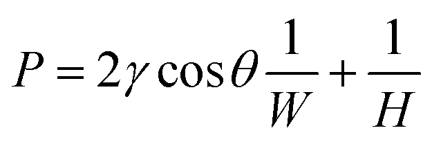
Fig. 1(a) shows the schematic for the fabrication process. First, the SU8 (MicroChem, USA) moulds for the texture pattern (SU8-2005) and microfluidic structures (SU8-2050) were fabricated on the wafers using standard soft lithography processes.48 The height of the texture pattern is only 5 μm in height, which will prevent LM from entering the texture structure later. Then PDMS (Sylgard 184 silicone elastomer kit, Dow Corning, USA) fabricated by mixing the base solution with the curing agent in a ratio of 10![[thin space (1/6-em)]](https://www.rsc.org/images/entities/char_2009.gif) :1 was poured onto the two SU8 moulds. The mass of the PDMS used for moulding can be determined by the required thickness of the chip. After the PDMS naturally spread on the mould, the PDMS and wafers were placed on a hot plate and baked at 75 °C for 2 h. Then, the cured PDMS slabs with textured pattern and microfluidic structures were peeled off from the wafer. After that, the two PDMS slabs were bonded face to face after standard air plasma treatment. Finally, LM were injected into the microfluidic structure easily without leaking into the texture slab because the texture pattern is too shallow. Fig. 1(b) shows the texture pattern under the microscope. Two kinds of texture structures were designed. One is composed of parallel straight ventilating microchannels and the other is composed of small squares. The parallel straight microchannels are 20 μm wide and spaced apart. The edge of the small squares is also 20 μm. Because of the low viscosity, photoresist SU8-2005 was used to fabricate the texture pattern structure with a mould height of only 5 μm and we had a correspond reason for choosing 5 μm as the height of the texture structure. The Young–Laplace equation for the liquid metal–air interface at the microchannel of this chip can be expressed as:49
:1 was poured onto the two SU8 moulds. The mass of the PDMS used for moulding can be determined by the required thickness of the chip. After the PDMS naturally spread on the mould, the PDMS and wafers were placed on a hot plate and baked at 75 °C for 2 h. Then, the cured PDMS slabs with textured pattern and microfluidic structures were peeled off from the wafer. After that, the two PDMS slabs were bonded face to face after standard air plasma treatment. Finally, LM were injected into the microfluidic structure easily without leaking into the texture slab because the texture pattern is too shallow. Fig. 1(b) shows the texture pattern under the microscope. Two kinds of texture structures were designed. One is composed of parallel straight ventilating microchannels and the other is composed of small squares. The parallel straight microchannels are 20 μm wide and spaced apart. The edge of the small squares is also 20 μm. Because of the low viscosity, photoresist SU8-2005 was used to fabricate the texture pattern structure with a mould height of only 5 μm and we had a correspond reason for choosing 5 μm as the height of the texture structure. The Young–Laplace equation for the liquid metal–air interface at the microchannel of this chip can be expressed as:49
 | (1) |
 | ||
| Fig. 1 (a) Texture structure and its chip fabrication process. (b) Schematic representation of two texture structures under the microscope. (Long rectangles and small squares, respectively). | ||
When using texture structures, we cut off the ends around the PDMS with texture structures before bonding the upper micropattern so that all microchannel structures are unsealed at both ends and directly connected to external atmospheric environment and the air can escape directly to the environment through these gaps when filling the liquid metal. In conclusion, this shallow design ensures that it only allows air to escape while preventing LM from leakage. The small square texture design has a much larger ventilating area than the straight channel design. These two texture structures can be chosen according to the actual chip structure and the ventilation requirements. The texture does not have to be spread all over the surface during the application, but can also be designed as needed. With the help of the ventilating texture structure, the microchannel for LM injection do not need outlets for the air to escape. Thus, the layout of the LM microchannel is largely simplified. In addition, we used a two-layer lithography technique to fabricate the texture structure and the microchannel structure into the same layer. The double-layer lithography and chip fabrication process is shown in Fig. S1 in the ESI.†
Results and discussion
Complex blind-end microstructure patterning
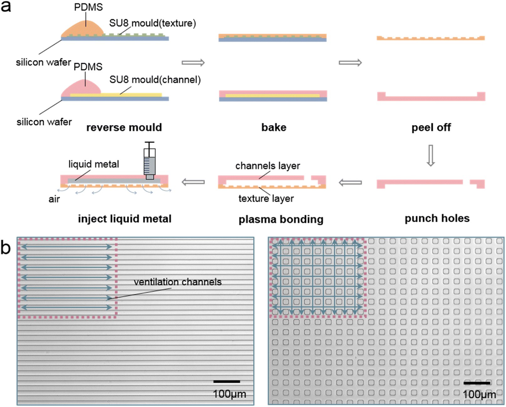
To verify that a microfluidic chip fabricated using texture structures can achieve blind-end injection of LM, we fabricated two microfluidic devices using blank PDMS and textured PDMS respectively. To ensure that the different results are caused only by the designed texture structure, the size of the microchannel and the thickness of the device (about 1 mm) are designed to be identical for both devices. The liquid metal injection effect of the two devices is shown in Fig. 2(a). Blank PDMS has poor air permeability. When there is only one inlet and no outlet, the LM is unable to expel the internal air in the microchannels. Therefore, there is a section of air remained at each end of the microchannel that prevents LM from filling the entire channel. In contrast, the device fabricated with texture structure does not suffer from above problems during the LM injection. Because the internal air can be freely expelled from the texture structure, the device with textured PDMS can be easily and quickly filled with LM by blind-end injection. As shown in Fig. 2(a) the filling was perfect even at the end of the microchannels.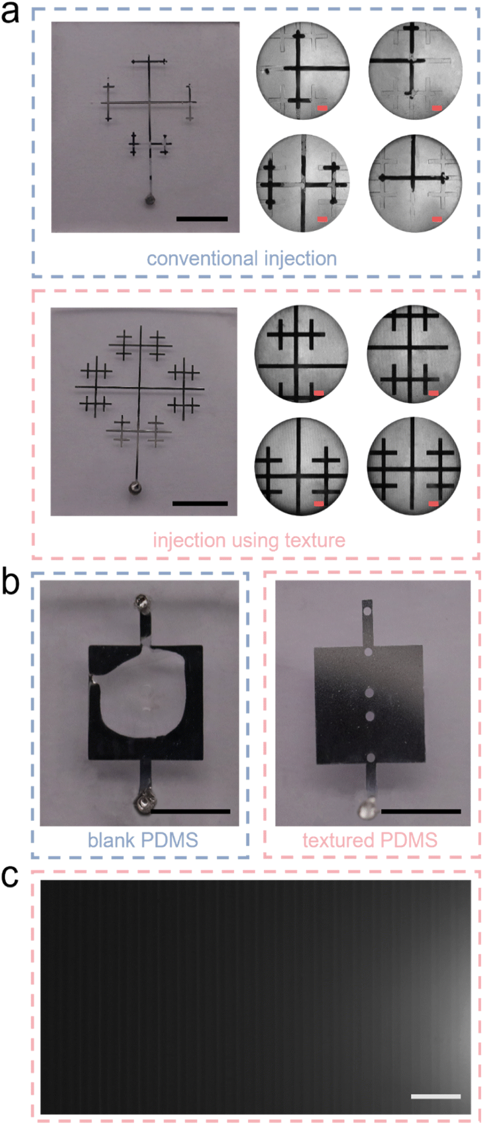 | ||
| Fig. 2 (a) Comparison of injections with a texture structure and blank PDMS using snowflake-like branching pattern. (b) Comparison of injections with a texture structure and blank PDMS using flat patterns with large aspect ratios. (c) Local magnification under the microscope in Fig. 2(b) “textured PDMS”. The black scale is 2 mm, the pink scale is 500 μm and the white scale is 100 μm. | ||
While being able to accomplish blind-end microstructure injection, the texture-aided technology also solves another problem that is often encountered in microfluidic chip fabrication, namely, self-collapse. This problem usually occurs when the aspect ratio (channel width/height) of the microchannel is too large.50 Since the height of microchannels obtained by soft lithography is usually tens of microns, this essentially limits the width of microchannels to the micron scale. When special texture structures are patterned on a PDMS slab, the textured surface can become unstick to other PDMS slabs after plasma treatment. To verify this, we designed a flat microchannel structure, which is 5.5 mm × 5.5 mm × 30 μm (length × width × height) in size and inverted it onto a PDMS slab about 2 mm thick. Then we bonded it with a blank PDMS slab and a textured PDMS slab respectively. After the injection of LM, the two microfluidic chips are shown in Fig. 2(b). In order to fill the flat microchannel with LM, we punched both the inlet and outlet for the device fabricated with blank PDMS, while only punched one inlet for the device fabricated with textured PDMS. We can see that the plate-like microchannel undergoes a large ceiling collapse during the plasma bonding on the blank PDMS at the center, and LM can only pass through the non-collapsed area. The channel fabricated with textured PDMS does not show any collapse bonding, and LM fills the whole flat channel completely. This is because the plate-like microchannel is not bonded to the textured surface of the PDMS slab, which has 20 μm wide grooves every 20 μm as shown in Fig. 2(c). We reflected on the reason of texture structures to avoid the phenomenon of self-collapse of high aspect ratio structure in the upper layer. We believe whether bonded to blank PDMS slab or PDMS with texture structures, collapse always occurs due to the high aspect ratio. The difference is that textured PDMS contains numerous microchannels with widths on the order of tens of microns. The bumpy surface, consisting of a dense array of microchannels, divides the upper high aspect ratio structure into multiple sections, significantly reducing the aspect ratio of each section, making it more difficult for the upper microstructure to contact the lower PDMS and bond when collapse occurs. Additionally, the texture structure in the lower layer corresponding to the upper high aspect ratio structure has a very small bonding area. Taking the square texture as an example, the PDMS area that may experience adhesion is only around 100 μm2, surrounded by recessed microchannels. According to our experimental results, if no excessive pressure is applied during bonding, the upper structure will not bond to such a small area of PDMS at all.
To further confirm the capability of texture structure for blind-end injection of LM in microfluidic devices, we designed several complex and characteristic micropatterns. The results obtained after their injection of LM are shown in Fig. 3. The dot marks the only inlet of each micropattern, and every detail of each pattern can be filled with LM completely. Fig. 3(a) shows a checkerboard grid structure. This is a typical structure with uniform channel width and a large number of intersections and branches. Fig. 3(b) shows the pattern obtained from a spiral coil after a toroidal array. This pattern does not have many branches, but the structure of spiral coil makes the distance from the inlet to the end of each microchannel much longer. Fig. 3(c) shows a typical branching structure that exists in nature. This structure also does not have many branches, but we designed both the petals and the leaves as hollow structures, which makes its minimum channel width only a few tens of microns. This also increases the difficulty of blind end injection to some extent. Fig. 3(d)–(f) shows three of the twelve Chinese zodiac signs-horse, dragon, and snake. These zodiac patterns not only have numerous branches but also vary widely in microchannel width. The widest channel can reach the millimeter scale, while the narrowest channel is only about twenty microns. Despite the complexity and variability of the microchannels that make up these patterns, LM can still fill each channel and structure. This fully demonstrates the advantages of texture structures for LM blind-end injection. This provides a new optional option for injecting blind-end microelectrodes. The use of PDMS itself to achieve air venting makes microfluidic devices more flexible in their integration and miniaturization.
 | ||
| Fig. 3 Complex blind-end microstructure injection using texture structures. (a) A checkerboard grid structure. (b) Spirals passing through a circular array. (c) Flower patterns in nature. (d) Horse pattern in the Chinese zodiac. (e) Dragon pattern in the Chinese zodiac. (f) Snake pattern in the Chinese zodiac. The black scale is 2 mm and the pink scale is 200 μm. | ||
The texture structure not only enables LM to fill the blind-end pattern, but even the filling speed is very impressive. In 2019, Wang et al. designed a porous sugar film for blind-end micropattern injection.37 They achieved blind-end injection of a tessellation pattern with a flow channel width of only 50 μm in 36 seconds. To compare the injection speed, we performed blind-end injection of the same pattern using the texture structure and found that the entire pattern could be injected in only 10 seconds, taking less than one-third of the original time (Movie S1, ESI†).
Parametric study of bonding properties
Despite there are many advantages of this textured structure, it also has an important problem. PDMS-based microfluidic devices usually require plasma treatment to be bonded together. This treatment actually uses the plasma to interact with the treated PDMS surface, which leads to modification of the PDMS surfaces and ultimately to bonding between PDMS surfaces. However, the presence of texture greatly reduces the surface area available for bonding. When texture size is too large and the surface area available for bonding is reduced to a certain extent, it may lead to bonding failure. Therefore, to investigate the effect of texture size on bonding, a parametric study was performed. We selected the designed texture consisting of small squares as the object of investigation. This is because the PDMS surface area available for bonding is smaller for this structure compared to the long rectangular structure with the same microchannel gap. We believe that the texture structure may affect the bonding results for two main reasons: (1) the unit area of each bondable small square and (2) the proportion of the sum of all bondable areas to the whole PDMS, as shown in Fig. 4(a). The gray area in the left-hand figure is the area of the unit's small square, and the ratio of all the grey areas to the pink boxes in the figure on the right is the ratio of the bondable area we are referring to. Considering the accuracy that can be achieved by lithography and the requirement that liquid metal cannot leak into the texture layer, we set the side length range of the unit square to be parameterized between 10 μm and 30 μm with an interval of 2.5 μm. Also, considering that the texture needs enough channels for air exhaust, we set the parameterization range for the ratio of bondable area to the total area between 10% and 50% with an interval of 5%. We subjected PDMS slabs with the same thickness but different side length of the squares to plasma treatment for the same time and tried bonding them with blank PDMS slabs separately, which also underwent the same plasma treatment. The results of parametric study are shown in Fig. 4(b). The blue dash represents the critical parameters of the texture structure that can be structurally bonded. The texture parameters represented by the green crosses below it indicate failed bonding, while the texture parameters represented by the orange circles above the blue dash indicate successful bonding. It shows that the success of bonding is indeed related to both the size of each unit square and the proportion of bondable area to the total area. When the size of the unit square is larger and the proportion of the bondable area to the total area is larger, the bonding is more likely to be successful. The two factors affect the results of bonding together and not independently of each other. For example, when the ratio of bondable area to total area is less than 45%, only textures with larger unit square size can be successfully bonded. However, when this ratio is greater than 45%, all square sizes within the parameterization range can be successfully bonded. This parametric research work provides a reference for future texture designs and provides a range of texture sizes that can be successfully applied to microfluidic devices.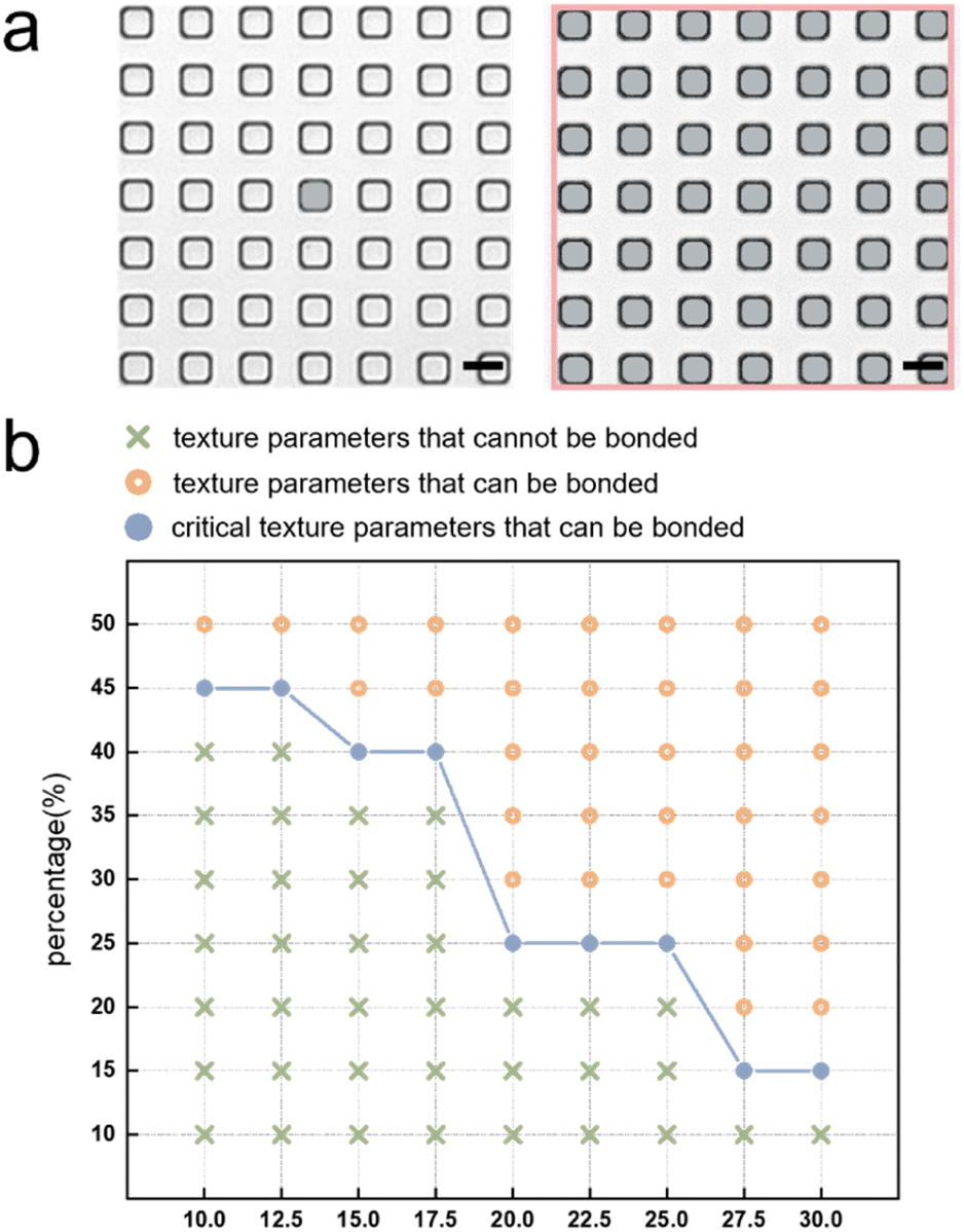 | ||
| Fig. 4 (a) Illustration of the concept of unit small square area and bondable area to total area. (b) Results of a parametric study on the effect of texture structure size on the bonding situation. The scale bar is 20 μm. | ||
Application of the texture structures: complex multi-layer chips
To demonstrate the necessity of structures in integrated multi-layer chips, we fabricated a multi-layer chip with three layers structure using the double-layer lithography technique described above. The three-layer structure is shown as Fig. 5(a). Fig. 5(b) shows the result of the multi-layer chip injected with LM. The chip consists of three structural layers and a substrate layer as shown in Fig. 5(c) and (d) (from top to bottom, the three structure layers are marked as the yellow, pink, and blue PDMS). The end of the structure of the upper layer overlaps with the initial inlet position of the structure of the lower layer and only the center of the top layer has an injection inlet for the whole chip. The injection process is shown in Movie S2.† By successfully injecting this blind-end chip, we demonstrate the excellent permeability of our proposed method in the vertical chip direction and the great potential for making multilayer chips. In addition, we applied the method to the fabrication of EOP. We designed an EOP with a three-layer structure. The structure of this EOP was improved compared with the one designed by Gao et al. in 2014.25 Since the means to achieve blind-end injection of LM in a microfluidic device was not available at that time, the electrodes of the EOP of Gao et al. used a “one inlet, one outlet” method to achieve LM penetration. However, this method made the electrode structure unnecessarily complex and the size of the whole device unnecessarily large. Using a texture structure, we reduced the size of the EOP driven by the same principle to 1 cm × 1 cm, which is much smaller than the original EOP size. We even realized the series connection of two pairs of driving electrodes in such a small size. The schematic of the EOP is shown in Fig. 6(a) and (b). It contains three layers, the bottom layer is the texture layer, and the other two layers are the channel layers. The middle layer contains the fluid channels, the electrode channels, and the channels that integrate the four electrodes connected to the same pole of the voltage. The top layer contains the channels for integrating the four electrodes of the other pole. This design allows the four pairs of electrodes to be connected to the positive and negative poles of the power supply with only one pair of inlets respectively. What should be pointed out is that, although the LM cannot leak from the texture surface because of its high surface tension, working fluid may leak from the textured surface. To avoid the leakage, we have designed the area of bottom texture. This texture structure avoids the working fluid channels and is designed only below the corresponding LM electrode channels. This ensures that the LM can be injected very easily into the four pairs of blind-end electrodes without interfering with the flow of fluid in the fluid channels. Deionized (DI) water was used as the pumping fluid for the experiment. The high voltage (higher than 60 V) to drive the electroosmotic pump is provided by a high voltage electrical sequence (HVS448 6000D, Labsmith). Low voltage (lower than 60 V) is provided by DC power 0.52 μm fluorescent particles were diluted 10000 times with DI water and used to measure the flow speed of the electroosmotic micropump. Zeiss Axio Observer, Z1 microscope (Oberkochen, Germany), and X-cite Series 120Q laser source (Excelitas Technologies, Waltham, MA, USA) are used to observe the movement of fluorescent particles in the flow channel.
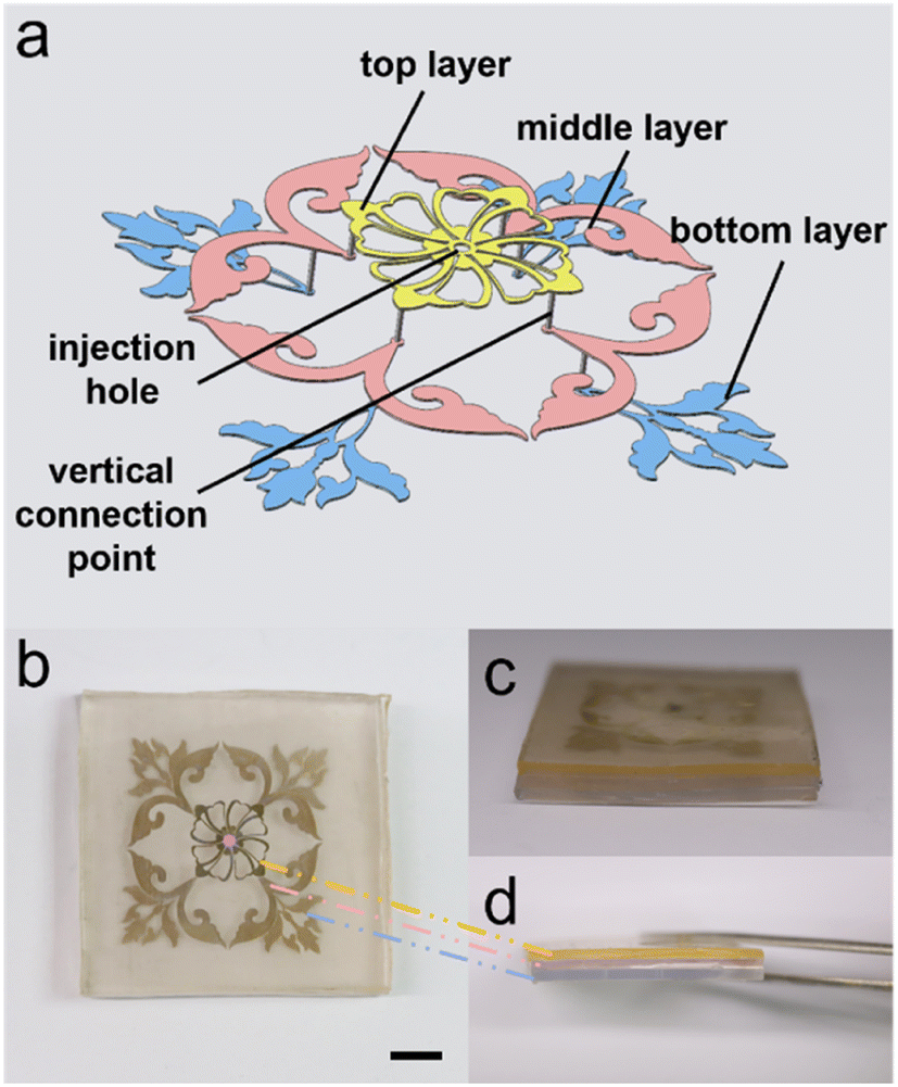 | ||
| Fig. 5 (a) Exploded view of the three layers structures. (b) Multilayer chip with blind-end infusion using texture structures. (c) Side view of the chip. (d) Schematic of the three layers of the chip. The black scale is 5 mm. | ||
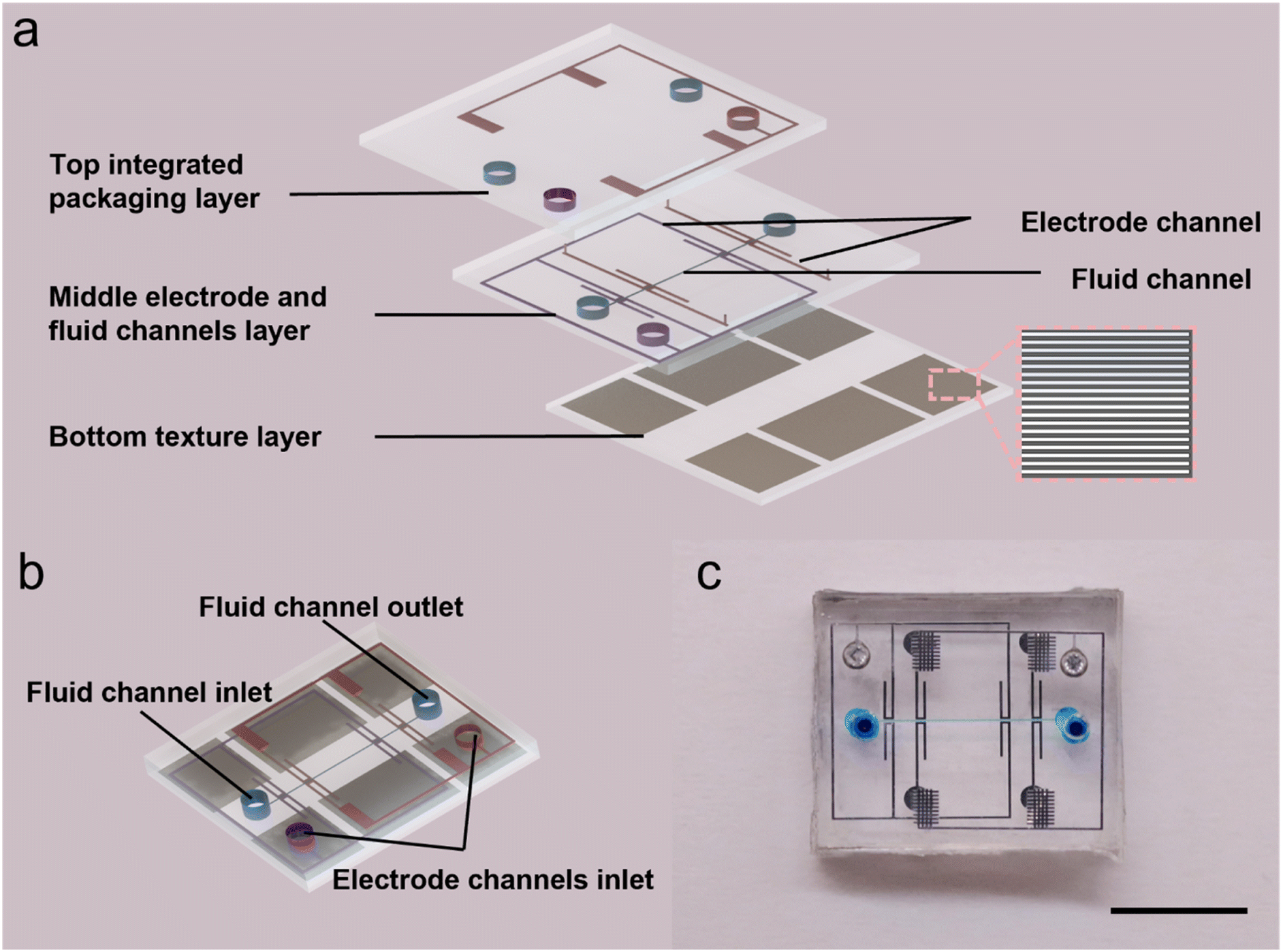 | ||
| Fig. 6 Schematic of the EOP (a) schematic of stratification of the EOP. (b) Combination of the EOP. (c) Actual schematic of EOP after injection. The black scale is 5 mm. | ||
Fig. 7(a) shows a sequential image of the movements of the fluorescent particles. The driving voltage between the electrodes is 80 V and the voltage on the left side of the image is positive. The four images were recorded sequentially at T = 0 s, 3 s, 6 s, and 9 s. We selected five specific particles in the flow channel and labelled them with the letters A–E. From the relative movement of the particle A–E positions, we can see the flow of the electroosmotic pump. In the actual measurement, we applied 10 different sets of voltages to the pump (from 10 V to 100 V with 10 V intervals). Each set of voltages was measured twice (once on the left side for positive voltage and once on the right side for positive voltage). We used python to process and calculate the relative movement of particles at different voltages. The final result of the flow rate is shown in Fig. 7(b). The relationship between the flow rate and the drive voltage can be approximated as a linear relationship. As the applied voltage increases, the flow rate of the fluid in the pump increases. The flow rate is 4.52 μm s−1 at 10 V, 34.72 μm s−1 at 100 V, and the lowest driving voltage is 3 V.
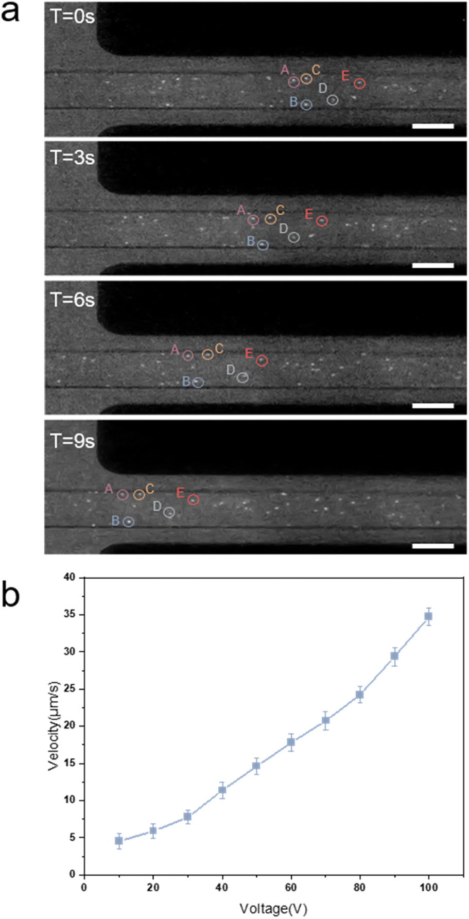 | ||
| Fig. 7 (a) Sequential diagram of the position of fluorescent particles in the flow channel at different times. (b) The flow rate of EOP at different voltages. The white scale is 50 μm. | ||
Conclusions
In this study, we have designed a texture structure based on a soft lithography fabrication. This structure can be directly inverted on PDMS so that the PDMS carries hundreds of open channels less than 20 μm wide. And we use SU8-2005 to control the height of these channels to less than 10 μm. In this way, when LM is injected into the PDMS chips, these texture structures consisting of open channels can quickly vent the air pressure inside the chip while ensuring that the LM does not leak into the texture. By this principle, we can achieve a fast and complete injection of LM in the microfluidic chips. In addition, using this PDMS with concave and convex texture structure instead of blank PDMS to fabricate microfluidic chips also solves the problem of the easy collapse of microstructures with a large aspect ratio. This opens up many new possibilities for the design of microelectrodes or other microstructures in the future. After verifying the possibility of this method on blind-end injection, we also did a parametric study on the effect of the size of the texture structure on the bonding situation. The parametric results show that both of our conjectured reasons affect the bonding situation. That is the unit area of each bondable small square and the proportion of the sum of all bondable areas to the whole PDMS. When the unit area of each square is larger and the proportion of the bondable area to the total area is larger, the bonding is more likely to be successful. Finally, we used this method to make a chip with a multi-layer blind-end pattern and then applied the structure to an EOP. It makes the electrode channels no longer need outlets and can fill several electrodes with liquid metal simultaneously through only one inlet. This change significantly reduces the size of the chip and increases its integration. In addition, this texture structure has a very prominent advantage over all previously proposed methods with blind-end injection. It achieves venting in the horizontal direction, rather than the vertical direction. This advantage offers the possibility to fabricate multilayer chips with blind-end structures in the future.Author contributions
Yuqing Li: conceptualization, data curation, formal analysis, investigation, methodology, validation, writing – original draft, writing – review & editing; Huimin Zhang: methodology, data curation, formal analysis; Yuqin Deng, Qian Li and Zi Ye: methodology and formal analysis. Lin Gui: conceptualization, methodology, validation, writing – review & editing, funding acquisition.Conflicts of interest
There are no conflicts to declare.Acknowledgements
This work is supported by the National Key Research and Development Program of China (2019YFB2204903), the Science and Technology Program from State Grid Corporation of China (no. 5700-202155453A-0-0-00) and the Director's Fund of Technical Institute of Physics and Chemistry.References
- A. Manz, N. Graber and H. M. Widmer, Sens. Actuators, B, 1990, 1, 244–248 CrossRef CAS.
- A. T. Conlisk, J. Fluid Mech., 2007, 570, 503 CrossRef.
- S. J. Maerkl and S. R. Quake, Science, 2007, 315, 233–237 CrossRef CAS PubMed.
- C. Ma, R. Fan, H. Ahmad, Q. Shi, B. Comin-Anduix, T. Chodon, R. C. Koya, C.-C. Liu, G. A. Kwong and C. G. Radu, Nat. Med., 2011, 17, 738–743 CrossRef CAS PubMed.
- Y. Zeng, M. Shin and T. Wang, Lab Chip, 2013, 13, 267–273 RSC.
- C.-C. Lee, G. Sui, A. Elizarov, C. J. Shu, Y.-S. Shin, A. N. Dooley, J. Huang, A. Daridon, P. Wyatt and D. Stout, Science, 2005, 310, 1793–1796 CrossRef CAS PubMed.
- J. S. Moore and K. F. Jensen, Org. Process Res. Dev., 2012, 16, 1409–1415 CrossRef CAS.
- S. Guven, J. S. Lindsey, I. Poudel, S. Chinthala, M. D. Nickerson, B. Gerami-Naini, U. A. Gurkan, R. M. Anchan and U. Demirci, Stem Cells Transl. Med., 2015, 4, 261–268 CrossRef PubMed.
- S. Cheng and Z. G. Wu, Lab Chip, 2010, 10, 3227–3234 RSC.
- H. J. Koo, J. H. So, M. D. Dickey and O. D. Velev, Adv. Mater., 2011, 23, 3559–3564 CrossRef CAS PubMed.
- Z. Ye, R. C. Zhang, M. Gao, Z. S. Deng and L. Gui, Micromachines, 2019, 10, 112–121 CrossRef PubMed.
- J. Gong, Q. Wang, B. Liu, H. Zhang and L. Gui, Micromachines, 2021, 12, 1051 CrossRef PubMed.
- L. F. Zhu, B. Wang, S. Handschuh-Wang and X. C. Zhou, Small, 2020, 16, 1903841 CrossRef CAS PubMed.
- G. H. Wagner and W. H. Gitzen, J. Chem. Educ., 1952, 29, 162 CrossRef CAS.
- N. N. Greenwood, in Advances in Inorganic Chemistry and Radiochemistry, ed. H. J. Emeléus and A. G. Sharpe, Academic Press, 1963, vol. 5, pp. 91–134 Search PubMed.
- W. Wilkinson, Properties of Gallium. Summary of Published Data on Alloys, Physical Properties and Chemistry, Argonne National Lab., Lemont, Ill., 1948 Search PubMed.
- K. E. Spells, Proc. Phys. Soc., 1936, 48, 299–311 CrossRef CAS.
- X. D. Zhang, X. H. Yang, Y. X. Zhou, W. Rao, J. Y. Gao, Y. J. Ding, Q. Q. Shu and J. Liu, Energy Convers. Manage., 2019, 185, 248–258 CrossRef.
- J. N. Koster, Cryst. Res. Technol., 1999, 34, 1129–1140 CrossRef CAS.
- K. Ling, K. Kim and S. Lim, Opt. Express, 2015, 23, 21375–21383 CrossRef CAS PubMed.
- A. J. Downs, Chemistry of Aluminium, Gallium, Indium and Thallium, 1992 Search PubMed.
- D. Zrnic and D. S. Swatik, J. Less-Common Met., 1969, 18, 67–68 CrossRef CAS.
- D. R. Lide, CRC Handbook of Chemistry and Physics, 87th edn, 2007 Search PubMed.
- B. T. Zhu, Y. F. Cai, Z. T. Wu, F. Z. Niu and H. Yang, IEEE Access, 2019, 7, 152224–152232 Search PubMed.
- M. Gao and L. Gui, Lab Chip, 2014, 14, 1866–1872 RSC.
- Y. C. Zheng, K. Kang, F. C. Xi, H. Y. Li and M. Gao, BioChip J., 2019, 13, 217–225 CrossRef CAS.
- M. Gao, L. Gui and J. Liu, J. Heat Transfer-Trans. ASME, 2013, 135, 091402 CrossRef.
- J. Je and J. Lee, J. Microelectromech. Syst., 2014, 23, 1156–1163 Search PubMed.
- R. C. Zhang, Z. Ye, M. Gao, C. Gao, X. Zhang, L. Li and L. Gui, Lab Chip, 2020, 20, 496–504 RSC.
- M. Gao and L. Gui, J. Micromech. Microeng., 2016, 26, 075005 CrossRef.
- K. L. Peng, J. Y. Yao, S. Cho, Y. Cho, H. S. Kim and J. Park, Sens. Actuators, A, 2020, 305, 111909 CrossRef CAS.
- S. I. H. Shah and S. Lim, Sensors, 2018, 18, 2935 CrossRef PubMed.
- A. Dey and G. Mumcu, IEEE Antennas Wirel. Propag. Lett., 2016, 15, 226–229 Search PubMed.
- R. D. P. Wong, J. D. Posner and V. J. Santos, Sens. Actuators, A, 2012, 179, 62–69 CrossRef CAS.
- M. L. Li, L. Zheng, T. B. Xu, H. L. Wo, U. Farooq, W. Q. Tan, C. Q. Bao, X. Z. Wang, S. R. Dong, W. Guo, J. K. Luo and J. M. Kim, Sens. Actuators, A, 2018, 279, 424–432 CrossRef CAS.
- J. B. Chossat, Y. W. Tao, V. Duchaine and Y. L. Park, IEEE, Seattle, WA, 2015.
- Y. Lin, C. Cooper, M. Wang, J. J. Adams, J. Genzer and M. D. Dickey, Small, 2015, 11, 6397–6403 CrossRef CAS PubMed.
- C. Ladd, J. H. So, J. Muth and M. D. Dickey, Adv. Mater., 2013, 25, 5081–5085 CrossRef CAS PubMed.
- Z. Z. He, J. Yang and J. Liu, Sci. Rep., 2014, 4, 4588 CrossRef PubMed.
- S. H. Jeong, K. Hjort and Z. G. Wu, Sensors, 2014, 14, 16311–16321 CrossRef PubMed.
- H. Cui, C. Cheng, J. Wu and S. Eda, 2013.
- B. A. Gozen, A. Tabatabai, O. B. Ozdoganlar and C. Majidi, Adv. Mater., 2014, 26, 5211–5216 CrossRef CAS PubMed.
- Y. L. Lin, O. Gordon, M. R. Khan, N. Vasquez, J. Genzer and M. D. Dickey, Lab Chip, 2017, 17, 3043–3050 RSC.
- W. Guo, A. J. T. Teo, A. M. Ganan-Calvo, C. L. Song, N. T. Nguyen, H. D. Xi and S. H. Tan, Phys. Rev. Appl., 2018, 10, 054045 CrossRef CAS.
- J. Hong, J. H. Gong, Q. Li, Z. S. Deng and L. Gui, Lab Chip, 2021, 21, 4566–4573 RSC.
- R. H. Wang, L. Gui, L. J. Zhang, Z. Z. He, M. Gao, S. Chen, X. Y. Zhou, Y. T. Cui and Z. S. Deng, Adv. Mater. Technol., 2019, 4, 1900256 CrossRef CAS.
- Z. Ye, Q. Li, R. C. Zhang, P. Zhang and L. Gui, RSC Adv., 2022, 12, 8290–8299 RSC.
- Y. N. Xia and G. M. Whitesides, Abstr. Pap. Am. Chem. Soc., 1997, 214, 348 Search PubMed.
- M. D. Dickey, R. C. Chiechi, R. J. Larsen, E. A. Weiss, D. A. Weitz and G. M. Whitesides, Adv. Funct. Mater., 2008, 18, 1097–1104 CrossRef CAS.
- Y. G. Xue, D. Kang, Y. J. Ma, X. Feng, J. A. Rogers and Y. G. Huang, Extreme Mech. Lett., 2017, 11, 18–23 CrossRef.
Footnote |
| † Electronic supplementary information (ESI) available. See DOI: https://doi.org/10.1039/d3ra04497a |
| This journal is © The Royal Society of Chemistry 2023 |