DOI:
10.1039/D3RA04176J
(Paper)
RSC Adv., 2023,
13, 23211-23222
Numerical simulation of lead-free vacancy ordered Cs2PtI6 based perovskite solar cell using SCAPS-1D†
Received
21st June 2023
, Accepted 15th July 2023
First published on 1st August 2023
Abstract
In recent years, vacancy-ordered halide double perovskites have emerged as promising non-toxic and stable alternatives for their lead-based counterparts in optoelectronic applications. In particular, vacancy ordered Cs2PtI6 has emerged as a star material because of its high absorption coefficient, band gap of 1.37 eV, and long minority carrier lifetime. Despite substantial experimental research on this new class of material, theoretical simulations of their device properties remain scarce. In this work, a novel n-i-p device architecture (FTO/SnO2/Cs2PtI6/MoO3/C) is theoretically investigated using a solar cell capacitance simulator (SCAPS-1D). Theoretical investigations are carried out in order to optimize the device performance structure by varying the perovskite and selective charge transport layer thickness, absorber and interface defect density, operating temperature, back contact, series and shunt resistance, respectively. The optimized device showed an impressive power conversion efficiency (PCE) of 23.52% at 300 K, which is higher than the previously reported values. Subsequent analysis of the device's spectral response indicated that it possessed 98.9% quantum efficiency (QE) and was visibly active. These findings will provide theoretical guidelines for enhancing the performance of Cs2PtI6-based photovoltaic solar cells (PSCs) and pave the way for the widespread implementation of environmentally benign and stable perovskites.
1 Introduction
In recent years, there has been an increasing interest in hybrid perovskite solar cells (HPSCs) due to their remarkable intrinsic properties, including lower production costs, higher carrier mobilities, tunable band gaps, long carrier diffusion lengths, and high absorption coefficient.1–4 In just over a decade, the PCE has dramatically increased from 3.3% to 25.7% due to the synergistic optimization of device interfaces. Full industrialization of HPSCs, in spite of having achieved a PCE of over 25% is trammeled by two main issues: Pb toxicity and instability. Organic ions methyl ammonium (MA+) and formamidinium (FA+) at the ‘A’ site of perovskite are unstable and degrade in atmospheric operational conditions.5–10 Consequently, it would be highly advantageous for device lifetimes and environmental and health considerations regarding production and reprocessing to seek out non-toxic and stable perovskites that sustain high efficiency. Materials such as (MA, Cs, Rb)3Sb2I9, Cs2PdBr6, Cs2AgBiBr6, Cs2AgBiI6, Cs2TiBr6, AgBiI4, CsGe0.5Sn0.5I3, and Cs2Au2I6 have been explored as lead-free alternatives, but their performance for photovoltaic applications has been disappointing.11–21
Finding stable, non-toxic, and highly efficient perovskites has proven to be an enormous problem to date. In recent years, A2BX6 (A![[double bond, length as m-dash]](https://www.rsc.org/images/entities/char_e001.gif) Cs; BTe, Sn, Pt, Ti; XI) double perovskites have garnered the attention of numerous researchers. These lead-free double perovskites demonstrate good stability and appropriate band gaps, making them viable candidates for future solar cell applications. As one of the most extensively studied vacancy-ordered halide double perovskites, Cs2SnI6 is a defect version of the three-dimensional (3D) CsSnI3 perovskite with half of the Sn atoms in the Sn-centered octahedron absent. In the fabrication of solar cells, the inefficiency of Cs2SnI6 is a problem. Cs2SnI6-based solar cells have an efficiency of approximately 1.5%, while Cs2SnI4Br2-based solar cells with mixed halides have an efficiency of 2.025%.
Cs; BTe, Sn, Pt, Ti; XI) double perovskites have garnered the attention of numerous researchers. These lead-free double perovskites demonstrate good stability and appropriate band gaps, making them viable candidates for future solar cell applications. As one of the most extensively studied vacancy-ordered halide double perovskites, Cs2SnI6 is a defect version of the three-dimensional (3D) CsSnI3 perovskite with half of the Sn atoms in the Sn-centered octahedron absent. In the fabrication of solar cells, the inefficiency of Cs2SnI6 is a problem. Cs2SnI6-based solar cells have an efficiency of approximately 1.5%, while Cs2SnI4Br2-based solar cells with mixed halides have an efficiency of 2.025%.
Cs2PtI6 is one of the intriguing materials in the A2BX6 class. Cs2PtI6 is an ideal option for PSCs due to its higher carrier mobility, higher absorption coefficient (4 × 105 cm−1), narrow band gap (1.37 eV), and dynamically stable structure.22 With a tolerance factor of 0.97, it is able to have a highly consistent cubic structure, hence increasing its stability. It is stable under harsh conditions, including high temperatures, UV light, and high humidity.23 It could serve as an appropriate substitute for perovskite-containing lead due to its oxidation resistance, high atomic number, and stability beyond non-toxicity. Cs2PtI6 is a highly advantageous photovoltaic material due to all of these qualities.
Unfortunately, systematic simulation and device modeling for the properties of Cs2PtI6 perovskite, which are essential for their optoelectronic devices, are rarely investigated, resulting in subpar device performance. To further improve the performance of Cs2PtI6-based PSCs, it is required to construct a band structure that minimizes charge recombination while enhancing carrier separation and transport. For this objective, device simulation is used to gain a comprehensive understanding of the relationship between the properties of materials and performance parameters. Using SCAPS-1D, a novel n-i-p device architecture (FTO/SnO2/Cs2PtI6/MoO3/C) is theoretically investigated in this work. Theoretical investigations were conducted to optimize the performance structure of the device by varying the thickness of the perovskite and selective charge transport layer, the absorber and interface defect density, the operating temperature, the back contact, the series and shunt resistance, respectively. At 300 K, the improved device demonstrated an outstanding PCE of 23.52%, which is greater than the previously reported figures. These findings will provide theoretical recommendations for boosting the performance of Cs2PtI6-based PSCs and pave the way for the broad adoption of environmentally friendly and stable perovskites.
2 Theoretical simulation
For our numerical simulations, we used SCAPS-1D software version 3.3.10. In SCAPS-1D a total of seven layers, along with different front and back contacts, could be employed as input. One can analyze J–V characteristics, ac characteristics (C–f and C–V), device efficiency (η), open circuit voltage (Voc), fill factor (FF), short circuit current density (Jsc), spectral response (QE) of device using SCAPS-1D. The simulations are based on three equations: Poisson's eqn (1) and continuity equation for holes and electrons eqn (2):| |
 | (1) |
where ψ is electrostatic potential, n and p are electron and hole concentrations, εo is vacuum and εr is relative permittivity, ND and NA are donor and acceptor doping density, ρn, ρp are electrons and holes distribution,| |
 | (2) |
where G is generation rate and R is recombination rate, Jp and Jn are holes and electron current densities.
Carrier transport occurs according to drift and diffusion equations:
| |
 | (3) |
| |
 | (4) |
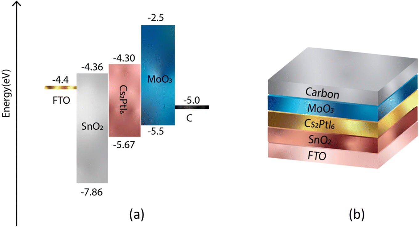
In order to achieve a higher level of efficiency, the hole transport layer (HTL) and electron transport layer (ETL) must have band gap edges that correspond with the VBM and CBM of the active layers. Fig. 1 and 2 illustrate the band gap alignment of MoO3, SnO2, and Cs2PtI6, as well as the back and front device contacts. The lowest unoccupied molecular orbital (LUMO) of SnO2 (ETL) is in excellent alignment with the conduction band of Cs2PtI6. Likewise, the highest occupied molecular orbital (HOMO) of MoO3 (HTL) is well-aligned with the valence band level of an absorbing material.
 |
| | Fig. 1 (a) Energy level diagram of FTO, ETL (SnO2), perovskite (Cs2PtI6), HTL (MoO3), back contact C (b) a schematic of device structure of n-i-p FTO/SnO2/Cs2PtI6/MoO3/C under AM 1.5 spectra, constant illumination 1000 W m−2, working temperature 300 K, shunt resistance 4200 Ω cm2 and series resistance 1 Ω cm2. | |
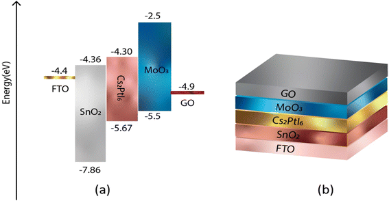 |
| | Fig. 2 (a) Energy level diagram of FTO, ETL (SnO2), perovskite (Cs2PtI6), HTL (MoO3), back contact GO (b) a schematic of device structure of n-i-p FTO/SnO2/Cs2PtI6/MoO3/GO under AM 1.5 spectra, constant illumination 1000 W m−2, working temperature 300 K, shunt resistance 4200 Ω cm2 and series resistance 1 Ω cm2. | |
Table 1 displays the input parameters for FTO, SnO2, Cs2PtI6, and MoO3 derived from the literature. The work functions of front contact (FTO) and back contact (carbon) are 4.4 eV and 5.0 eV, respectively. Thermal velocity of both holes and electrons is 1 × 10⁷ (at 300 K). For all defects, defect type is taken as neutral, characteristic energy is 1.0 eV, energetic distribution is single. Defect density for both interfaces is 1 × 10¹³, capture cross-section of electrons and holes is 1 × 10¹⁸. All simulations were performed under AM 1.5 spectra, constant illumination 1000 W m−2, working temperature 300 K, shunt resistance 4200 Ω cm2 and series resistance 1 Ω cm2.
Table 1 Input parameters for materials used in the device architecture FTO/SnO2/Cs2PtI6/MoO3/C
| Input parameters |
FTO |
n-SnO2 |
Cs2PtI6 |
n-MoO3 |
| Thickness, d (nm) |
500 |
10 |
300 |
30 |
| Band gap, Eg (eV) |
3.5 |
3.5 |
1.37 |
3 |
| Electron affinity, χ |
4 |
4 |
4.3 |
2.5 |
| Permittivity, εr |
9 |
9 |
4.8 |
12.5 |
| Electron mobility, μn (cm2 V−1 s−1) |
20 |
20 |
62.6 |
25 |
| Hole mobility, μp (cm2 V−1 s−1) |
10 |
10 |
62.6 |
100 |
| Effective density of states at CB, Nc (cm−3) |
2.2 × 10¹⁸ |
2.2 × 10¹⁷ |
3.0 × 10¹⁴ |
2.2 × 10¹⁸ |
| Effective density of states at VB, Nv (cm−3) |
1.8 × 10¹⁹ |
2.2 × 10¹⁶ |
1.0 × 10¹⁷ |
1.8 × 10¹⁹ |
| Density of n-type doping, ND (cm−3) |
1 × 10¹⁹ |
1 × 10¹⁸ |
1 × 10¹² |
0 |
| Density of p-type doping, NA (cm−3) |
0 |
0 |
1 × 10¹⁵ |
1 × 10⁻¹⁸ |
| Defect density, Nt (cm−3) |
— |
1 × 10¹⁵ |
1 × 10¹⁷ |
1 × 10¹⁵ |
| Capture cross-section electron (cm2) |
— |
2 × 10⁻¹⁴ |
1 × 10⁻¹⁵ |
1 × 10⁻¹⁵ |
| Capture cross-section holes (cm2) |
— |
2 × 10⁻¹⁴ |
1 × 10⁻¹⁵ |
1 × 10⁻¹⁵ |
| Reference |
24 |
25 |
23 and 26 |
27 |
3 Result and discussion
3.1 Effect of HTL thickness
To ensure that the same number of charge carriers reach terminals instantaneously with a low recombination probability, the thickness of the HTL is generally higher than that of the electron transport layer. In general, the recombination rate increases as the HTL's thickness decreases. Fig. 3 illustrates the impact of HTL thickness on device properties. Here, MoO3 thickness ranged from 20 to 100 nm. Both Voc and Jsc increased with increasing MoO3 thickness (Table S1†), reaching saturation at 32 nm with a maximum of 26.163 mA cm−2 and 1.14 V, respectively. Both PCE and FF increased with increasing thickness until reaching a maximum value, after which they reduced till reaching a constant value.
 |
| | Fig. 3 Influence of varying MoO3 (HTL) thickness (20–100 nm) on device performance of configuration FTO/SnO2/Cs2PtI6/MoO3/C PSC (a) comparison of PCE and FF, (b) comparison of Voc and Jsc. | |
When the HTL thickness is too thin, current leakage and low shunt resistance can occur, resulting in a lower FF.28 In our case, it decreased after reaching the highest FF value of 80.44% at 22 nm. It could be because increasing HTL thickness increased series resistance, causing the FF to drop to 75.74% at 60 nm before remaining unchanged.28 At 24 nm, the maximum efficiency of 23.13%, Voc of 1.118 V, Jsc of 26.158 mA cm−2, and FF of 79.105% was obtained. Thus, the optimum HTL thickness of 24 nm was utilized for our subsequent devices.
3.2 Effect of absorbing layer thickness
In designing a solar cell, the thickness of the perovskite is crucial because it directly affects the device parameters. Because electron–hole pair generation occurs in the absorbing layer, increasing thickness increases incident light absorption and generates more electron–hole pairs. This increases the device's PCE, but only up to a certain point, after which efficiency degrades. In this case, the perovskite thickness should not exceed the carrier diffusion length; otherwise, recombination and back contact recombination density would increase. The influence of absorbing layer thickness on PCE, Jsc, Voc, and FF is shown in Fig. 4 and Table S2†. Here, the Cs2PtI6 thickness was varied from 100 nm to 1000 nm. Jsc increased as perovskite thickness increased. Because Cs2PtI6 has a higher absorption coefficient (4 × 105 cm−1),22 increasing thickness allows more light to be absorbed, resulting in more electron–hole pair generation. Although the length of charge carrier diffusion in these perovskites is also longer, these electron–hole pairs can reach the corresponding electrodes to generate power.29 The Jsc at 680 nm reached a maximum of 30.37 mA cm−2 before decreasing. These findings are consistent with previously reported data.30
 |
| | Fig. 4 Impact of changing Cs2PtI6 (absorber layer) thickness (100–1000 nm) on performance of cell configuration FTO/SnO2/Cs2PtI6/MoO3/C PSC (a) PCE and FF, (b) Voc and Jsc, (c) comparison of J–V curves at different Cs2PtI6 thicknesses. | |
PCE also increased as the thickness increased, but only up to 400 nm, where the maximum efficiency of 23.8% is observed, and then it decreased. As a result of a higher absorption coefficient, a higher number of charge carriers are generated, resulting in the maximum possible increase in efficiency. Following this optimal thickness, PCE decreased. Despite the higher level of electron and hole generation, the perovskite thickness exceeds the carrier diffusion length of electrons and holes, resulting in increased recombination rates and decreased efficiency. When thickness increases, so do pinholes, cracks, and traps, resulting in a decline in PCE.29
Voc increased with perovskite thickness until it reached a maximum of 1.11 V at 260 nm, after which it dropped precipitously. Voc is defined as:
where
n is an ideality factor,
q is the electrical charge,
T is temperature,
k is the Boltzmann constant,
Io is the dark saturation current, and
IL is light generated current.
Voc is affected by cracks, pinholes, and other layer defects and is dependent on surface morphology. The absorber layer is relatively thinner during the early increase in
Voc, resulting in a lower recombination rate. Furthermore, as the length of the diffusion carrier increases, so does the value of the dark saturation current. This slower recombination rate eventually leads to a higher concentration of carriers, which raises the light-generated current
IL. However, as the thickness of the absorbing layer continues to increase, the recombination rate, along with
Io, increases, causing the
Voc to fall abruptly and squarely.
29 The FF relates to charge route resistance and represents the efficiency with which holes and electrons transit the cell without loss.
31,32 As the perovskite's thickness increased, the fill factor decreased. FF decreased from 78.3% at 100 nm to 43.29% at 1000 nm as the thickness increased.
3.3 Effect of ETL thickness
The dependence of solar cell properties on ETL (SnO2) was studied by varying the thickness of the electron transport layer from 10 nm to 100 nm (Table S3 †). To prevent incident photons from being absorbed and producing electron–hole pairs in the electron transport layer, it is common to practice keeping the n-type layer (ETL) thinner than the equivalent p-type layer (HTL). ETL is also kept thinner to allow incident photons to pass through to the absorber and HTLs beneath it. The influence of ETL thickness change on cell metrics is depicted in Fig. 5. By increasing ETL thickness, no improvement in cell metrics was observed. PCE, Voc, Jsc, and FF were 23.52%, 1.11782 V, 26.95 mA cm−2, and 78.076% at 10 nm, and 23.49%, 1.11780 V, 26.93 mA cm−2, and 78.078% at 100 nm, respectively. With the increase in ETL thickness, the change in Voc was insignificant (from 1.11782 V to 1.11780 V, a loss of just 0.0017%), indicating that by varying the thickness of SnO2 ETL, charge carrier leakage at the interface is limited. When the thickness of a device grows, fewer electron–hole pairs are formed, and charge carrier recombination occurs, resulting in a drop in overall device efficiency. Our optimal device has an ETL thickness of 10 nm, with PCE of 23.52%, Jsc of 26.95 mA cm−2, Voc of 1.1178 V, and FF of 8.076%.
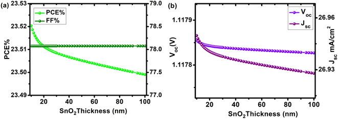 |
| | Fig. 5 Device performance of configuration FTO/SnO2/Cs2PtI6/MoO3/C PSC as a function of increasing SnO2 (ETL) thickness (10–100 nm) (a) PCE and FF, (b) Voc and Jsc. | |
3.4 Perovskite (absorber) layer defect density
The optoelectronic properties of an absorbent layer are highly dependent on its preparation method, thickness, and analysis methodologies. Furthermore, defects in the system could change the optoelectronic properties. Defects were introduced into the absorbent layer to make our device appear more realistic. The defect density ranged from 1014–1020 cm−3. Fig. 6 depicts the effect of Cs2PtI6 defect density on cell parameters. The recombination rate increases and all cell characteristics decrease as the number of cracks and pinholes increases due to an increase in Nt. An efficiency of 26% was observed with a defect density of 1 × 1015 cm−3. We chose a defect density of 1 × 1017 cm−3 for our device, which yielded an efficiency of 23.5% (Table 2). Material defects must be reduced in order for the device to be effective, and it must be smooth and free of cracks.
 |
| | Fig. 6 Effect of Cs2PtI6 (absorber layer) defect density (1014–1020 cm−3) on device parameters of cell configuration FTO/SnO2/Cs2PtI6/MoO3/C (a) PCE and FF, (b) Voc and Jsc, (c) a comparison of J–V curves of device at different absorber layer defect densities. | |
Table 2 Solar cell parameters at various Cs2PtI6 (perovskite absorber layer) defect densities (Nt) for configuration FTO/SnO2/Cs2PtI6/MoO3/C
| Defect density(cm−3) |
Voc (V) |
Jsc (mA cm−2) |
FF (%) |
PCE (%) |
| 1 × 10¹⁴ |
1.1287 |
27.0396 |
85.37 |
26.05 |
| 1 × 10¹⁵ |
1.1286 |
27.0788 |
85.29 |
26.03 |
| 1 × 10¹⁶ |
1.1275 |
27.0307 |
84.55 |
25.77 |
| 1 × 10¹⁷ |
1.1178 |
26.9497 |
78.08 |
23.52 |
| 1 × 10¹⁸ |
1.0560 |
26.1602 |
58.83 |
16.25 |
| 1 × 10¹⁹ |
0.8291 |
19.9050 |
38.68 |
6.38 |
| 1 × 10²⁰ |
0.6708 |
4.6933 |
27.87 |
0.88 |
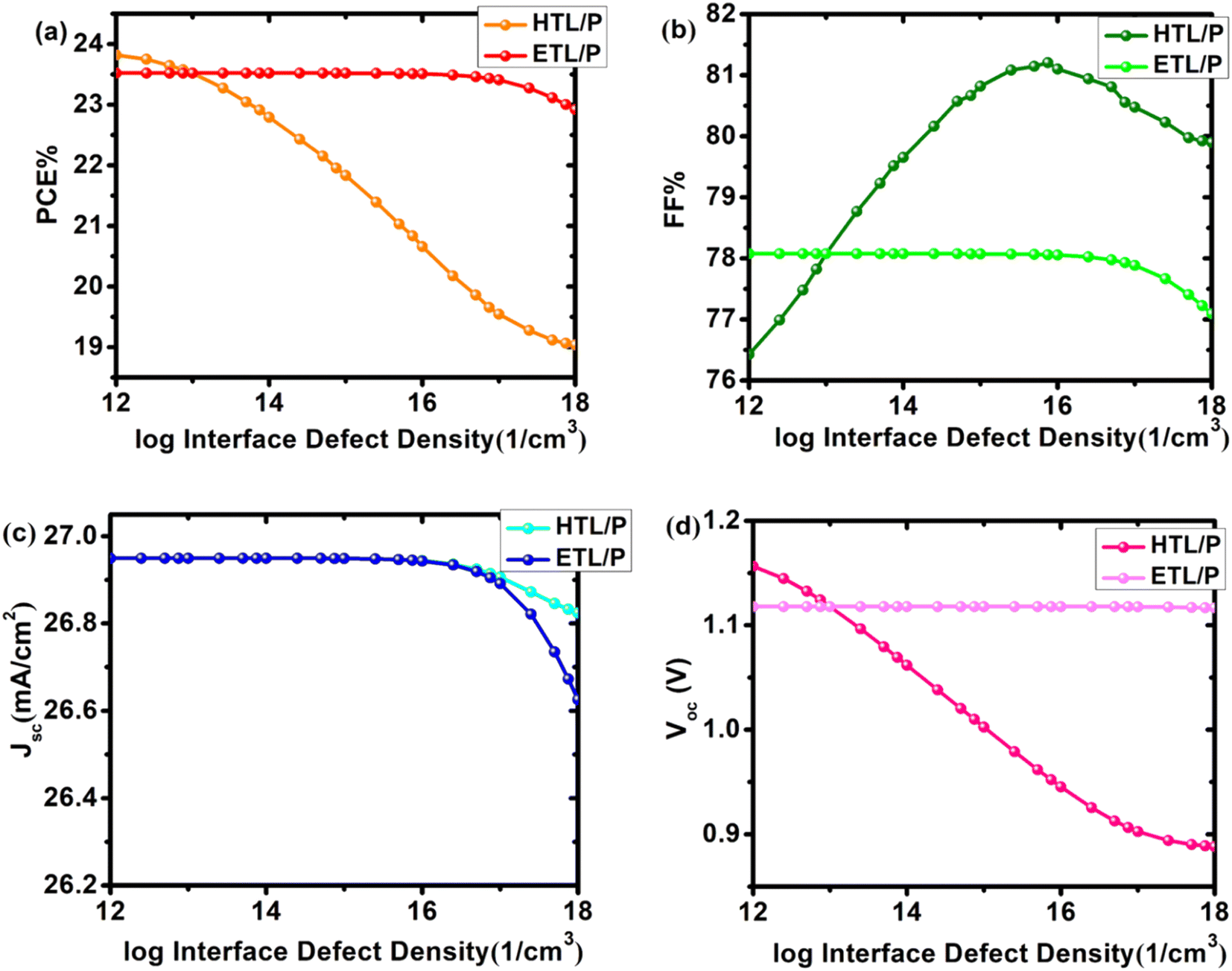
3.5 Effect of interface defect density
Due to a mismatch in the crystallographic structures of the ETL, HTL, and absorbing layer, interfaces with a plethora of dislocations could form, hence reducing junction quality and triggering recombination. The defect density was varied between 1012 cm−3 and 1018 cm−3 to explore the global impact of interface defect density on cell performance. Fig. 7 depicts the impact of interface defect density on cell characteristics. There was no significant change in PCE and Voc when the defect density of the ETL/perovskite layer (SnO2/Cs2PtI6) was varied (Table S4 †). However, with the increase in the interface defect density of the HTL/perovskite layer (MoO3/Cs2PtI6), the efficiency and Voc drastically degraded (Table S5 †). The cell's PCE decreased from 23.8% at 1012 Nt to 19.04% at 1018 Nt. Voc tumbled by 23%, from 1.156 V to 0.888 V.
 |
| | Fig. 7 Solar cell output as a function of varying defect density Nt (1012–1018 cm−3) of interfaces MoO3/Cs2PtI6 (HTL/P) and SnO2/Cs2PtI6 (ETL/P) of device configuration FTO/SnO2/Cs2PtI6/MoO3/C (a) efficiency (PCE), (b) fill factor (FF), (c) short circuit current Jsc and (d) open circuit voltage Voc. | |
As Nt increases, there is no discernible change in Jsc. It only decreases when the prevalence of interface defects increases. By increasing the Nt of the HTL/P layer to 1018 cm−3 (from 26.94 mA cm−2 to 26.62 mA cm−2), Jsc decreased by 1.19%. Both interfaces have an effect on the fill factor. The fill factor decreased from 78.08% to 77.08% when ETL/perovskite defects increased. In the case of the HTL/perovskite layer, the defect density increased from 76.42% to an all-time high of 81.2% at Nt 1015 cm−3, before decreasing to 79.90% at defect density 1018 cm−3. We have selected a defect density of 1013 cm−3for both device interfaces.
3.6 Effect of temperature
Temperature has a direct effect on hole mobility, electron mobility, and carrier concentration, all of which affect cell performance.33 The device's performance was investigated at temperatures ranging from 290 K to 400 K. Eqn (5) shows the effect of temperature on Voc:34| |
 | (5) |
where Voc is open circuit voltage, K is Boltzmann constant, q is the electronic charge, n is ideality constant, T is temperature, Jo is reverse saturation current and Jsc is current density. It has been observed that with the increase in the operating temperature, reverse saturation current density increases, and Voc decreases exponentially.35 Fig. 8 and Table S6† depict the effect of temperature on device performance. All cell metrics degraded with each increase in temperature. Voc decreased from 1.12295 V at 290 K to 1.02557 V at 400 K. The FF decreased from 78.31% to 69.98%. There was no discernible change in the device's current density. It decreased by 0.09% from 26.9536 to 26.9282 mA cm−2. The device's PCE fell from 23.7% to 19.0%. As the temperature rises, the phonons are triggered, increasing charge carrier scattering, this modifies the material's conductivity. As a result, overall performance declined. For our device, we have chosen an optimal working temperature of 300 K where PCE is 23.52%, Voc is 1.11782 V, Jsc is 26.9519 mA cm−2 and FF is 78.07%.
 |
| | Fig. 8 Influence of changing operating temperature (290–400 K) on parameters of cell configuration FTO/SnO2/Cs2PtI6/MoO3/C (a) PCE and FF, (b) Voc and Jsc, (c) a comparison of J–V curves of device at different temperatures. | |
3.7 Effect of resistance on device parameters
Device performance is immensely influenced by both series and shunt resistance. Series resistance is due to interfaces, back and front contact, and resistance to flow of current while Rsh is the aftereffect of reverse saturation current. Both high Rsh and low Rs are likely to deliver better device performance. The effect of Rs and Rsh on device parameters was studied by altering values between 0.01–50 Ω cm2and 10–10000 Ω cm2. Eqn (6) can be used to understand the effect of resistance on device performance:34| |
 | (6) |
where Isc is short circuit current, Rsh is shunt resistance, Rs is series resistance, IL is light induced current, and IO is reverse saturation current.
According to the above equation, when series resistance increases, short circuit current will decrease. This would have a direct effect on the device's efficiency and FF. The impact of series and shunt resistance on device parameters is seen in Fig. 9. PCE and FF drop as Rs increases, but Jsc is only affected at higher Rs levels and Voc is unaffected. At Rs 0.01 Ω cm2, a PCE high of 24.1% is measured. PCE dropped to 6.03% as the value of Rs increased from 0.01 to 50 Ω cm2. Similar to PCE, the fill factor decreased from 79.9% to 25.57% (Table 3). The initial increase in resistance had little effect on the Jsc, but at 50 Ω cm2, it decreased from 26.959 mA cm−2 to 21.068 mA cm−2. In case of Rsh, both PCE and FF increased with an increase in Rsh but only at low Rs, Voc isn't much affected by Rsh while Jsc increased with increase in Rsh. These findings are consistent with those of other researchers. Hence, for improved device performance, the series resistance should be kept low while shunt resistance should be kept high.
 |
| | Fig. 9 Device parameters as function of increases resistance Rs (0.01 to 50 Ω cm2) of cell configuration FTO/SnO2/Cs2PtI6/MoO3/C (a) PCE, (b) FF, (c) Voc and (d) Jsc. | |
Table 3 Solar cell parameters at different values of series resistance RS (Ω cm2) for configuration FTO/SnO2/Cs2PtI6/MoO3/C
| Series resistance (Rs) (Ω cm2) |
Voc (V) |
Jsc (mA cm−2) |
FF (%) |
PCE (%) |
| 0.01 |
1.11770 |
26.959 |
79.99 |
24.10 |
| 0.1 |
1.11771 |
26.958 |
79.81 |
24.05 |
| 1 |
1.11782 |
26.949 |
78.07 |
23.52 |
| 5 |
1.11805 |
26.908 |
70.45 |
21.19 |
| 10 |
1.11815 |
26.847 |
61.26 |
18.39 |
| 25 |
1.11820 |
26.501 |
38.02 |
11.27 |
| 40 |
1.11827 |
24.528 |
27.12 |
7.44 |
| 50 |
1.11830 |
21.068 |
25.57 |
6.03 |
3.8 Quantum efficiency studies
Quantum efficiency (QE) is the probability that an incident photon will transfer an electron to the device's external circuit. Yet, this property is independent of the incident spectrum. Fig. 10 demonstrates the effect of absorbing layer thickness on quantum efficiency for wavelengths between 300 and 900 nm. QE increased with increasing perovskite thickness up to a maximum of 98.9% before declining. At 100 nm, the QE was 70%. At 400 nm, the concentration increased from 91.6% at 200 nm to 98.85%. A further increase in thickness did not result in a significant increase in QE, as QE at 500 nm was already 98.9%. QE decreased to 86.1% at 1000 nm as thickness rose further. In the range of 354–550 nm, high quantum efficiency was observed. As its thickness increased, its wavelength range changed towards longer values. Maximum QE was observed at the same wavelength (354.5 nm) for perovskite thicknesses between 100 nm and 600 nm, however as thickness increased, this wavelength shifted to longer wavelengths. The high QE of perovskite is due to its high absorption coefficient (4 × 105 cm−1).22 This study demonstrates that Cs2PtI6 is optically active and may have additional applications in photovoltaics.
 |
| | Fig. 10 Quantum efficiency of device configuration FTO/SnO2/Cs2PtI6/MoO3/C at different Cs2PtI6 thicknesses (100–1000 nm). | |
3.9 Effect of back contact on device parameters
The back contact of solar cells is essential to their performance because it absorbs electrons from the absorbing layer. For ohmic contact with the HTL or the absorber layer, a high work function is necessary. Fig. 9 illustrates the effect of the back contact work function on the device's properties. Cu, Ni, Ag, Fe, GO, and C were used as back contact materials in our device. As work function increased, efficiency grew, beginning at 13.14% with Cu as the back contact and reaching a high of 23.52% with carbon as the back contact. The other cell metrics likewise improved when the back contact's work function increased. As the work function of the back contact increases, the barrier height for charge carriers at the back contact decreases, leading to an overall improvement in cell characteristics. Table 4 compares cell properties to the work function of the back contact (Fig. 11 and 12).
Table 4 Solar cell parameters at different values of back contact work function (eV) for configuration FTO/SnO2/Cs2PtI6/MoO3/C
| Back contact |
Work function (Φ) |
Voc (V) |
Jsc (mA cm−2) |
FF (%) |
PCE (%) |
| Cu36 |
4.53 |
0.72 |
26.822 |
67.60 |
13.14 |
| Ni37 |
4.61 |
0.80 |
26.861 |
69.85 |
15.04 |
| Ag38 |
4.74 |
0.92 |
26.905 |
73.11 |
18.14 |
| Fe39 |
4.81 |
0.98 |
26.921 |
74.94 |
19.80 |
| GO40 |
4.9 |
1.05 |
26.937 |
76.98 |
21.94 |
| C41 |
5.0 |
1.12 |
26.949 |
78.08 |
23.52 |
 |
| | Fig. 11 Device performance as a function of back contact work function for cell configuration FTO/SnO2/Cs2PtI6/MoO3/C (a) PCE and FF, (b) Voc and Jsc, (c) J–V curve of device with different back contacts. | |
 |
| | Fig. 12 J–V curves of the optimized device having configuration (a) FTO/SnO2/Cs2PtI6/MoO3/C and (b) FTO/SnO2/Cs2PtI6/MoO3/GO. | |
4 Conclusion
We have reported the design optimization of an ecologically friendly, lead-free planar Cs2PtI6 solar cell using MoO3 as the HTL and SnO2 as the ETL (Table 5). Our research demonstrates that MoO3 (HTL), Cs2PtI6, and SnO2 have a considerable effect on device performance. The impact of varying the defect densities of the interface and absorber layers demonstrated that these parameters are crucial for device performance and that fewer defects are necessary for improved device performance. It was determined that series resistance had little influence on Voc but a substantial effect on PCE, FF, and Jsc. Effect of shunt resistance showed that both PCE and FF increase with an increase in Rsh (at low Rs), Voc isn't much affected by Rsh while Jsc increases with an increase in Rsh. In addition, the effect of temperature on the device's functionality revealed that lower temperatures led to improved performance. The material's spectral response revealed that it was active. Cu, Ni, Ag, Fe, Go, and C were employed as back contacts, with C's work function of 5.0 eV being the best. The optimal device was the n-i-p device with the structure FTO/SnO2/Cs2PtI6/MoO3/C with a PCE of 23.52% (Voc of 1.118 V, Jsc of 26.95 mA cm−2, FF of 78.08%).
Table 5 Performance comparison of our work and preceding work on Cs2PtI6 based PSCs
| Device architecture |
Voc (V) |
Jsc (mA cm−2) |
FF (%) |
PCE (%) |
Experimental/simulation |
Reference |
| ITO/SnO2/Cs2PtI6/spiro-OMeTAD/Au |
0.73 |
1.20 |
82.00 |
0.72 |
Experimental |
23 |
| FTO/CdS/Cs2PtI6 with EDA/carbon/Cu |
1.07 |
19.84 |
65.03 |
13.88 |
Experimental |
22 |
| FTO/CdS/Cs2PtI6/carbon/Cu |
1.20 |
20.20 |
41.51 |
10.06 |
Experimental |
22 |
| FTO/ZnO/Cs2PtI6/MoO3/Cu |
1.3856 |
16.1070 |
75.54 |
16.85 |
Simulation |
26 |
| FTO/ZnO/Cs2PtI6/MoO3/C |
1.4105 |
16.1122 |
90.01 |
20.45 |
Simulation |
26 |
| FTO/CdS/Cs2PtI6/MoO3/Cu |
1.11 |
20.14 |
61 |
13.9 |
Simulation |
30 |
| FTO/CdS/Cs2PtI6/Cu2O/Cu |
1.1 |
20.4 |
62 |
14.2 |
Simulation |
30 |
| FTO/CdS/Cs2PtI6/CuI/Cu |
1.12 |
20.13 |
60 |
13.7 |
Simulation |
30 |
| FTO/ICZSO/ Cs2PtI6/Cu2O/C |
1.13 |
22.2 |
59.2 |
14.8 |
Simulation |
30 |
| FTO/ZnSe/Cs2PtI6/Cu2O/C |
1.12 |
22.3 |
58 |
14.7 |
Simulation |
30 |
| FTO/WS2/Cs2PtI6/Cu2O/C |
1.1 |
28.1 |
52.4 |
16.3 |
Simulation |
30 |
| FTO/SnO2/Cs2PtI6/MoO3/GO |
1.05 |
26.94 |
76.99 |
21.95 |
Simulation |
This work |
| FTO/SnO2/Cs2PtI6/MoO3/C |
1.118 |
26.95 |
78.08 |
23.52 |
Simulation |
This work |
Conflicts of interest
There are no conflicts to declare.
References
- H. Y. F. Chen, W. T. Tang, J. J. He, M. S. Yin, Y. B. Wang, F. X. Xie, E. B. Bi, X. D. Yang, M. Gratzel and L. Y. Han, Nature, 2017, 550, 92–95, DOI:10.1038/nature23877.
- Z. Wang, et al., Efficient ambient-air-stable solar cells with 2D–3D heterostructured butylammonium-caesium-formamidinium lead halide perovskites, Nat. Energy, 2017, 2(9), 1–10, DOI:10.1038/nenergy.2017.135.
- G. E. Eperon, et al., Formamidinium lead trihalide: a broadly tunable perovskite for efficient planar heterojunction solar cells, Energy Environ. Sci., 2014, 7(3), 982–988, 10.1039/C3EE43822H.
- Z. Shi, et al., Strategy of solution-processed all-inorganic heterostructure for humidity/temperature-stable perovskite quantum dot light-emitting diodes, ACS Nano, 2018, 12(2), 1462–1472, DOI:10.1021/acsnano.7b07856.
- M. Jeong, et al., Large-area perovskite solar cells employing spiro-Naph hole transport material, Nat. Photonics, 2022, 16(2), 119–125, DOI:10.1038/s41566-021-00931-7.
- R. Lin, et al., All-perovskite tandem solar cells with improved grain surface passivation, Nature, 2022, 603(7899), 73–78 CrossRef CAS PubMed . https://www.nature.com/articles/s41586-021-04372-8.
- K. Xiao, et al., All-perovskite tandem solar cells with 24.2% certified efficiency and area over 1 cm2 using surface-anchoring zwitterionic antioxidant, Nat. Energy, 2020, 5(11), 870–880, DOI:10.1038/s41560-020-00705-5.
- S. D. Stranks and H. J. Snaith, Metal-halide perovskites for photovoltaic and light-emitting devices, Nat. Nanotechnol., 2015, 10(5), 391–402, DOI:10.1038/nnano.2015.90.
- M. T. Hörantner and H. J. Snaith, Predicting and optimizing the energy yield of perovskite-on-silicon tandem solar cells under real world conditions, Energy Environ. Sci., 2017, 10(9), 1983–1993, 10.1039/C7EE01232B.
- T. A. Berhe, et al., Organometal halide perovskite solar cells: degradation and stability, Energy Environ. Sci., 2016, 9(2), 323–356, 10.1039/C5EE02733K.
- E. Jokar, et al., Robust tin-based perovskite solar cells with hybrid organic cations to attain efficiency approaching 10%, Adv. Mater., 2019, 31(2), 1804835, DOI:10.1002/adma.201804835.
- M. Chen, et al., Cesium titanium (IV) bromide thin films based stable lead-free perovskite solar cells, Joule, 2018, 2(3), 558–570, DOI:10.1016/j.joule.2018.01.009.
- S. Weber, et al., Influence of the iodide to bromide ratio on crystallographic and optoelectronic properties of rubidium antimony halide perovskites, ACS Appl. Energy Mater., 2018, 2(1), 539–547, DOI:10.1021/acsaem.8b01572.
- Y. Hu, et al., Enhancing moisture-tolerance and photovoltaic performances of FAPbI3 by bismuth incorporation, J. Mater. Chem. A, 2017, 5(48), 25258–25265, 10.1039/C7TA08824H.
- F. Umar, et al., Dimensionality controlling of Cs3Sb2I9 for efficient all-inorganic planar thin film solar cells by HCl-assisted solution method, Adv. Opt. Mater., 2019, 7(5), 1801368, DOI:10.1002/adom.201801368.
- W. Dai, et al., Lead-free, stable, and effective double FA4GeIISbIIICl12 perovskite for photovoltaic applications, Sol. Energy Mater. Sol. Cells, 2019, 192, 140–146, DOI:10.1016/j.solmat.2018.12.031.
- B. W. Park, et al., Bismuth based hybrid perovskites A3Bi2I9 (A: methylammonium or cesium) for solar cell application, Adv. Mater., 2015, 27(43), 6806–6813, DOI:10.1002/adma.201501978.
- A. Kulkarni, et al., Performance enhancement of AgBi2I7 solar cells by modulating a solvent-mediated adduct and tuning remnant BiI 3 in one-step crystallization, Chem. Commun., 2019, 55(28), 4031–4034, 10.1039/C9CC00733D.
- E. Greul, et al., Highly stable, phase pure Cs2AgBiBr6 double perovskite thin films for optoelectronic applications, J. Mater. Chem. A, 2017, 5(37), 19972–19981, 10.1039/C7TA06816F.
- K. Ahmad, et al., A (CH3NH3)3Bi2I9 Perovskite Based on a Two-Step Deposition Method: Lead-Free, Highly Stable, and with Enhanced Photovoltaic Performance, ChemElectroChem, 2019, 6(4), 1192–1198, DOI:10.1002/celc.201801322.
- L. Debbichi, et al., Mixed valence perovskite Cs2Au2I6: a potential material for thin-film Pb-free photovoltaic
cells with ultrahigh efficiency, Adv. Mater., 2018, 30(12), 1707001, DOI:10.1002/adma.201707001.
- D. Schwartz, et al., Air Stable, High-Efficiency, Pt-Based Halide Perovskite Solar Cells with Long Carrier Lifetimes, Phys. Status Solidi – Rapid Res. Lett., 2020, 14(8), 2000182, DOI:10.1002/pssr.202000182.
- S. Yang, et al., Novel lead-free material Cs2PtI6 with narrow bandgap and ultra-stability for its photovoltaic application, ACS Appl. Mater. Interfaces, 2020, 12(40), 44700–44709, DOI:10.1021/acsami.0c11429.
- E. Karimi and S. Ghorashi, Investigation of the influence of different hole-transporting materials on the performance of perovskite solar cells, Optik, 2017, 130, 650–658, DOI:10.1016/j.ijleo.2016.10.122.
- N. Lakhdar and A. Hima, Electron transport material effect on performance of perovskite solar cells based on CH3NH3GeI3, Opt. Mater., 2020, 99, 109517, DOI:10.1016/j.optmat.2019.109517.
- M. Shamna and K. Sudheer, Device modeling of Cs2PtI6-based perovskite solar cell with diverse transport materials and contact metal electrodes: a comprehensive simulation study using solar cell capacitance simulator, J. Photonics Energy, 2022, 12(3), 032211, DOI:10.1117/1.JPE.12.032211.
- W. Li, et al., Numerical analysis of the back interface for high efficiency wide band gap chalcopyrite solar cells, Sol. Energy, 2019, 180, 207–215, DOI:10.1016/j.solener.2019.01.018.
- L. Lin, et al., Numerical analysis of inverted-structure perovskite solar cell based on all-inorganic charge transport layers, J. Photonics Energy, 2019, 9(2), 024501, DOI:10.1117/1.JPE.9.024501.
- K. Tan, et al., Controllable design of solid-state perovskite solar cells by SCAPS device simulation, Solid-State Electron., 2016, 126, 75–80, DOI:10.1016/j.sse.2016.09.012.
- H. H. AbdElAziz, et al., Evaluating the performance of Cs2PtI6−xBrx for photovoltaic and photocatalytic applications using first-principles study and SCAPS-1D simulation, Heliyon, 2022, 8(10), e10808, DOI:10.1016/j.heliyon.2022.e10808.
- S. Ahmed, et al., Simulation studies of Sn-based perovskites with Cu back-contact for non-toxic and non-corrosive devices, J. Mater. Res., 2019, 34(16), 2789–2795, DOI:10.1557/jmr.2019.204.
- A. Hagfeldt, et al., Dye-sensitized solar cells, Chem. Rev., 2010, 110(11), 6595–6663, DOI:10.1021/cr900356p.
- S. Hossain, et al., A numerical study on the prospects of high efficiency ultra thin znx cd1−x s/cdte solar cell, Chalcogenide Lett., 2011, 8(4), 263–272 Search PubMed.
- K. Chakraborty, M. G. Choudhury and S. Paul, Numerical study of Cs2TiX6 (X= Br−, I−, F− and Cl−) based perovskite solar cell using SCAPS-1D device simulation, Sol. Energy, 2019, 194, 886–892, DOI:10.1016/j.solener.2019.11.005.
- A. Fahrenbruch and R. Bube, Fundamentals of Solar Cells: Photovoltaic Solar Energy Conversion, Elsevier, 2012 Search PubMed.
- C. D. Zangmeister, et al., Energy-level alignment and work function shifts for thiol-bound monolayers of conjugated molecules self-assembled on Ag, Cu, Au, and Pt, Chem. Phys. Lett., 2007, 442(4–6), 390–393, DOI:10.1016/j.cplett.2007.06.012.
- W. Sachtler and G. Dorgelo, The surface of copper-nickel alloy films: I. Work function and phase composition, J. Catal., 1965, 4(6), 654–664, DOI:10.1016/0021-9517(65)90265-4.
- A. Dweydari and C. Mee, Work function measurements on (100) and (110) surfaces of silver, Phys. Status Solidi A, 1975, 27(1), 223–230, DOI:10.1002/pssa.2210270126.
- R. Wu and A. Freeman, Structural, electronic, and magnetic properties of an open surface: Fe (111), Phys. Rev. B: Condens. Matter Mater. Phys., 1993, 47(7), 3904, DOI:10.1103/PhysRevB.47.3904.
- J. P. Jayaraman, et al., BiVO4/Cs2PtI6 Vacancy-Ordered Halide Perovskite Heterojunction for Panchromatic Light Harvesting and Enhanced Charge Separation in Photoelectrochemical Water Oxidation, ACS Appl. Mater. Interfaces, 2021, 13(14), 16267–16278, DOI:10.1021/acsami.0c22654.
- M. Hamdan and A. K. Chandiran, Cs2PtI6 halide perovskite is stable to air, moisture, and extreme pH: application to photoelectrochemical solar water oxidation, Angew. Chem., 2020, 132(37), 16167–16172, DOI:10.1002/ange.202000175.
|
| This journal is © The Royal Society of Chemistry 2023 |
Click here to see how this site uses Cookies. View our privacy policy here. 
 Open Access Article
 This Open Access Article is licensed under a
  *c and
Zareen Akhter
*c and
Zareen Akhter