DOI:
10.1039/D3RA04051H
(Review Article)
RSC Adv., 2023,
13, 25968-25977
Engineering graphitic carbon nitride for next-generation photodetectors: a mini review
Received
16th June 2023
, Accepted 22nd August 2023
First published on 1st September 2023
Abstract
Semiconductor photodetectors, as photoelectric devices using optical–electrical signal conversion for detection, are widely used in various fields such as optical communication, medical imaging, environmental monitoring, military tracking, remote sensing, etc. Compared to the conventional photodetector materials including silicon, III–V semiconductors and metal sulfides, graphitic carbon nitride (g-C3N4) as a metal-free polymeric semiconductor, has many advantages such as low-price, easy preparation, efficient visible light response, and relatively good thermal stability. In the meantime, the polymer characteristics also endow the g-C3N4 with good mechanical properties. Apart from being used for photo(electro)catalysts during the past decades, the potential use of g-C3N4 in photodetectors has attracted great research interests very recently. In this review, we first briefly introduce the structure and properties of g-C3N4 and the key performance parameters of photodetectors. Then, combining the very recent progress, the review focuses on the active materials, fabrication methods and performance enhancement strategies for g-C3N4 based photodetectors. The existing challenges are discussed and the future development of g-C3N4 based photodetectors is also forecasted.
1. Introduction
Photodetectors, transforming light signals to electrical signals for detection and sensing, are very important optoelectronic devices that have been widely used in various areas such as light communication, medical imaging, environmental monitoring, military tracking, and remote sensing. Semiconductor materials, as the critical components in photodetectors, can generate electrons and holes when absorbing photons with energy higher than their bandgap. The separation of photo-generated electrons and holes can directly give rise to the variation of electrical conductivity, thereby resulting in conversion from optical signals to electrical signals. Currently, the commonly used light-sensitive material for commercial photodetectors is silicon. The growth of high-purity silicon, however, usually involves expensive instruments, complicated and energy-intensive processing technologies. Due to a small bandgap of 1.12 eV, addition of waveguide grating structures is necessary when using silicon for ultraviolet (UV) photodetectors, not only reducing the sensing area but also increasing the cost.1 In addition, the inherent rigidity and brittleness of crystalline silicon materials make it difficult to bend, rendering them unable to meet the requirements of next-generation flexible, foldable electronics even wearable devices. Compared to silicon, III–V compound semiconductors (such as gallium arsenide, GaAs) have a larger bandgap, which can be used for photodetectors with higher carrier mobility and lower power consumption. However, GaAs-based photodetectors also face challenges such as complex fabrication processes and limitations in large-scale applications due to the presence of toxic elements. In recent years, with the continuous progress in materials science, researchers have conducted in-depth studies on various materials including carbon nanotubes,2,3 graphene,4,5 two-dimensional (2D) transition metal compounds,4,6–8 perovskite materials,9–11 inorganic wide-bandgap semiconductors,12 and quantum dots.13,14 Significant progress has been made in improving the detection performance and optimizing device structures. Among them, it is of great significance to develop low-cost and easily fabricated photodetector devices based on organic optoelectronic materials.15,16
Graphitic carbon nitride (g-C3N4) is a metal-free polymeric semiconductor material. In 2009, a benchmark study disclosing the water splitting performance of g-C3N4 by Wang et al. offered exciting opportunities for the study on g-C3N4 materials.17 In the past decades, g-C3N4 has been widely used in diverse fields such as artificial photosynthesis,18 photoelectrochemical devices,19 biomedicine,20 sensors21 and optoelectronic devices.22 In general, g-C3N4, with good light response, thermal stability and mechanical property, can be prepared via a simple and cost-effective thermal polymerization/condensation of nitrogen-rich organic molecules. However, the physiochemical properties of g-C3N4 are mainly dependent on the polymerization degree due to the polymer characteristics. The conventional thermal polymerization derived g-C3N4 contains abundant defects within the inner structure, strongly affecting the intrinsic conductivity. In addition, the as-synthesized g-C3N4 is bulk material, which needs to be transferred onto conductive substrates via different post-treatments, hindering the large-scale application of g-C3N4 in electronic devices to a certain extent. Thanks to the development of material synthesis and device processing technology, researchers have fabricated ultrafast and highly-sensitive g-C3N4 based optoelectronic devices with broad prospect of application in detection and sensing areas.22
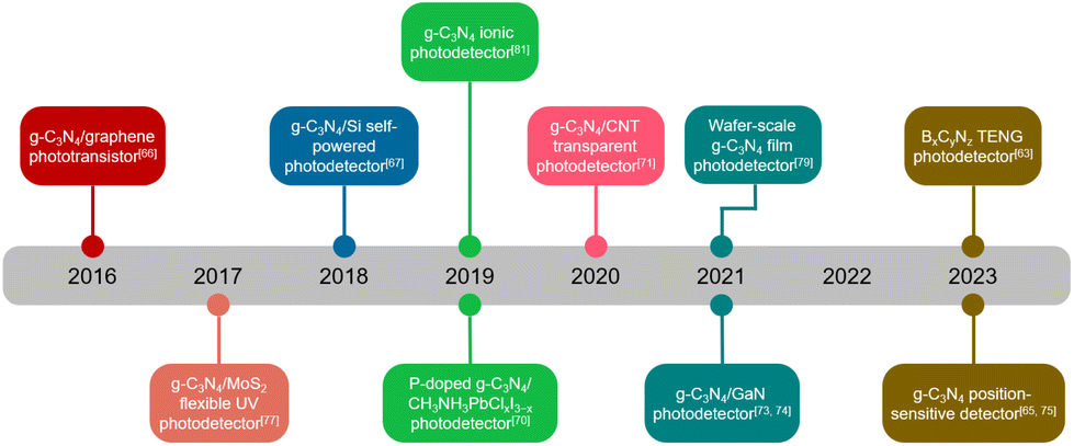
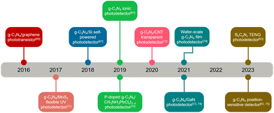
Scheme 1 shows the timeline of g-C3N4 for photodetector application since the first report in 2016. During the past seven years, researchers have developed different strategies to continuously optimize the performances of g-C3N4 based photodetectors. All these research progresses exemplify that g-C3N4 is a very promising materials for photodetectors, and the capability may arise from their intrinsic optical property and mechanical performance towards the practical devices. This review focuses on the latest research progress on g-C3N4 based photodetectors. First, the structure and basic characteristics of g-C3N4, as well as the main electrical performance parameters of photodetectors, are briefly introduced. Then, from the point of view of material and device design, the exploration of g-C3N4-based photodetectors and their performance regulation strategies are summarized in detail. Third, we analyze the existing issues of g-C3N4-based photodetectors and also discuss the research directions in the future.
 |
| | Scheme 1 The timeline of g-C3N4 for photodetector applications. | |
2. Structure and properties of graphitic carbon nitride
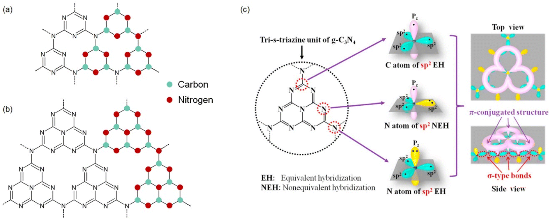
The discovery of carbon nitride can be traced back to the nineteenth century. In 1834, Liebig firstly synthesized carbon nitride materials and named it as ‘melon’.24 In 1922, Franklin proposed a concept of carbon nitride (C3N4) which was considered as the final product of melon after calcination.25 Pauling and Sturdivant first deduced that the coplanar tri-s-triazine units exist in the C3N4 structure in 1937.26 Using the first principle method, Teter and Hemley found the polymorphism of carbon nitride, which have five crystal structures including α-C3N4, β-C3N4, cubic C3N4, pseudo-cubic C3N4 and graphitic C3N4 (g-C3N4).27 Among these allotropes, g-C3N4 is a metal-free n-type semiconductor and has a graphite-like layered structure (space group: P![[6 with combining macron]](https://www.rsc.org/images/entities/char_0036_0304.gif) m2; a = b = 4.7420 Å, c = 6.7205 Å; α = β = 90°, γ = 120°),27 with interlayers connected by van der Waals forces, and it is most stable at ambient temperature and pressure. As shown in Fig. 1, g-C3N4 mainly has two chemical structures consisting of triazine (Fig. 1a) and tri-s-triazine (Fig. 1b) units respectively. Through density functional theory, Kroke et al. found that g-C3N4 with tri-s-triazine as structural units is more stable.28 Combining the X-ray diffraction and neutron diffraction, Irvine et al. proposed that the three-dimensional structure of g-C3N4 is formed by parallel chains of tri-s-triazine units following the A–B stacking order.29 In addition, both carbon and nitrogen atoms in g-C3N4 structure undergo sp2 hybridization, with overlapping sp2 hybrid orbitals forming σ bonds, while the overlapping 2pz orbitals form π bonds, ultimately creating a highly delocalized π-conjugated system (Fig. 1c).23 It should be noted that g-C3N4 has different chemical bonding when compared to nitrogen-doped carbon material. In general, the C–N bond length of g-C3N4 is ∼1.33 Å while two cases are different: (i) the C–N bond length ranges from 1.38 to 1.40 Å for the middle part of tri-s-triazine unit; (ii) the C–N bond length ranges from 1.45 to 1.48 Å for the tri-coordinated N atoms connecting three tri-s-triazine units.30 For nitrogen-doped graphene, the C–N bond length of N-substituted graphene is 1.41 Å except for pyridinic N and pyrrolic N, of which the bond lengths are 1.33–1.34 Å and 1.33/1.39 Å respectively.31
m2; a = b = 4.7420 Å, c = 6.7205 Å; α = β = 90°, γ = 120°),27 with interlayers connected by van der Waals forces, and it is most stable at ambient temperature and pressure. As shown in Fig. 1, g-C3N4 mainly has two chemical structures consisting of triazine (Fig. 1a) and tri-s-triazine (Fig. 1b) units respectively. Through density functional theory, Kroke et al. found that g-C3N4 with tri-s-triazine as structural units is more stable.28 Combining the X-ray diffraction and neutron diffraction, Irvine et al. proposed that the three-dimensional structure of g-C3N4 is formed by parallel chains of tri-s-triazine units following the A–B stacking order.29 In addition, both carbon and nitrogen atoms in g-C3N4 structure undergo sp2 hybridization, with overlapping sp2 hybrid orbitals forming σ bonds, while the overlapping 2pz orbitals form π bonds, ultimately creating a highly delocalized π-conjugated system (Fig. 1c).23 It should be noted that g-C3N4 has different chemical bonding when compared to nitrogen-doped carbon material. In general, the C–N bond length of g-C3N4 is ∼1.33 Å while two cases are different: (i) the C–N bond length ranges from 1.38 to 1.40 Å for the middle part of tri-s-triazine unit; (ii) the C–N bond length ranges from 1.45 to 1.48 Å for the tri-coordinated N atoms connecting three tri-s-triazine units.30 For nitrogen-doped graphene, the C–N bond length of N-substituted graphene is 1.41 Å except for pyridinic N and pyrrolic N, of which the bond lengths are 1.33–1.34 Å and 1.33/1.39 Å respectively.31
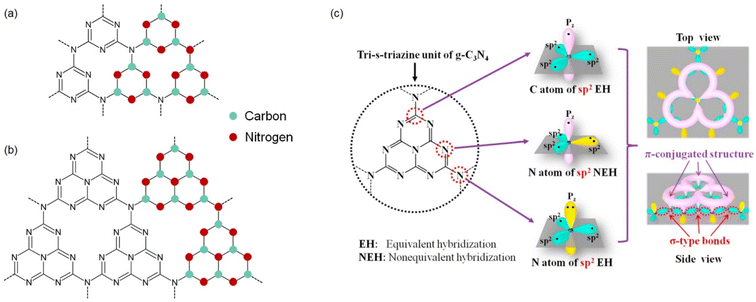 |
| | Fig. 1 Schematic illustration of chemical structure of g-C3N4: (a) triazine structure and (b) tri-s-triazine structure. (c) Hybrid structure and π-conjugated structure of the tri-s-triazine unit of g-C3N4. Reproduced from ref. 23 with permission. Copyright 2019, Elsevier. | |
In general, g-C3N4 can be prepared by the thermal condensation of nitrogen-containing molecules including urea, melamine, dicyandiamide, etc. However, different preparation conditions can yield triazine or tri-s-triazine based g-C3N4 products. This can be attributed to two aspects: (i) because triazine unit has a higher energy, it is thermodynamically difficult to synthesize g-C3N4 with pure s-triazine units.32 In comparison to g-C3N4 with s-triazine units only, poly(triazine imide) (PTI) which is prepared with the assistance of molten salts, is likely to be generated.33 (ii) Transforming triazine or tri-s-triazine units to highly condensed structure usually takes place above 520 °C.19 When the temperature is increased, the polymerization degree is very hard to control due to the release of ammonia. As the structure of g-C3N4 is highly disordered, a slight change in the experimental condition is likely to lead to different structural character.
Compared to silicon and metal compound semiconductor materials, g-C3N4 has the following advantages. First, directly heating nitrogen-containing organic molecules to achieve the polymerization is the most commonly used synthetic method to prepare g-C3N4 in a low-cost manner since the raw materials are earth-abundant and easily accessible. Second, with a bandgap of 2.7 eV, the light sensitivity of g-C3N4 is outstanding in particular in the UV range.34 Third, g-C3N4 has very excellent chemical stability and relatively good thermal stability. Fourth, as a polymer material with outstanding bending properties, g-C3N4 is also highly compatible with different polymer substrates for developing flexible, stretchable, and wearable devices. Table 1 compares the physical properties between g-C3N4 and several representative electronic materials for optoelectronic devices. Compared to other materials, g-C3N4 has a larger bandgap while the thermal conductivity and Young's modulus are comparable to that of silicon. However, the electron mobility of g-C3N4 is extremely low and the performance should be further optimized in order to meet the requirements of photodetector applications.
Table 1 Comparison of g-C3N4 and several representative materials for optoelectronic devices
| Materials |
Bandgap (eV) |
Electron mobility (cm2 V−1 s−1) |
Thermal conductivity (W cm−1 K−1) |
Young's modulus (GPa) |
Ref. |
| Si |
1.12 |
∼1400 |
∼1.42 |
130–169 |
35–38 |
| GaAs |
1.42 |
9000 |
0.435 |
85.6–115.9 |
39–42 |
| Graphene |
0 |
2 × 10⁵ |
5 × 10³ |
2400 ± 400 |
43–46 |
| MoS2 |
1.29 |
50–200 |
∼52 |
270 ± 100 |
47–50 |
| g-C3N4 |
2.7 (tri-s-triazine-based) |
0.089 |
3.5–7.6 |
171 |
17 and 51–54 |
| 3.2 (triazine-based) |
3. Main parameters of photodetectors
Although the semiconductor materials, device structures, and detection mechanisms vary for different types of photodetectors, their electrical performance can be quantitatively evaluated using key parameters such as switch ratio, responsivity, response time, signal-to-noise ratio, noise equivalent power, specific detectivity, external quantum efficiency, and gain.9,55–60 The following provides a brief introduction to the definitions and significance of each performance parameter.
3.1 On/off ratio
The ratio of the photocurrent (Ilight) under constant optical intensity, wavelength, and bias conditions to the dark current (Idark) without light irradiation. The magnitude of the on/off ratio serves as an important indicator of the photoresponse characteristics. For some semiconductors with a narrow bandwidth used as photodetectors, higher dark currents (when the device cannot be switched off completely) directly affect the switch ratio.
3.2 Responsivity (R)
The ratio of the output photocurrent (or photovoltage) to the incident optical power at a given wavelength, expressed as R(λ) = I(λ)ph/P(λ)in or R(λ) = V(λ)ph/P(λ)in, where I(λ)ph is the photocurrent, V(λ)ph is the photovoltage, and P(λ)in is the incident optical power. Responsivity represents the magnitude of the photocurrent (or photovoltage) generated per unit optical power and intuitively reflects the photodetectors' effectiveness in converting light to electric signals.
3.3 Response time
The response time refers to the time it takes for a photodetector to switch between dark current and photocurrent, reflecting its response ability to the changes of light signals. Typically, the response time can be defined as the time it takes for the photocurrent to rise from 10% to 90% (or fall from 90% to 10%) of its maximum steady-state value. When the photocurrent variation follows an exponential relationship, the response time can be defined as the time required for the photocurrent to increase to 63% (1 − 1/e ≈ 63%) of its steady-state peak value. The response time of different types of photodetectors primarily depends on the materials and detection mechanisms. For example, the response time of optoelectronic devices is related to carrier mobility, channel length, and bias voltage. The response time of photovoltaic devices depends on the thickness of the active layer and carrier mobility.56
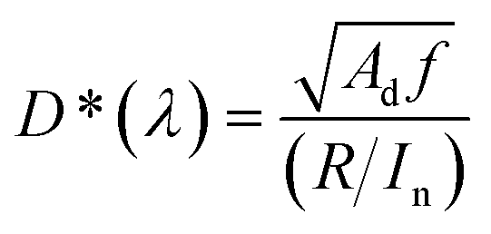
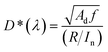
3.4 Specific detectivity (D*)
D* is the reciprocal of NEP. It was found that the NEP is related to the detectivity, detector area, and bandwidth.61 The D* is defined as the following equation:62| |
 | (1) |
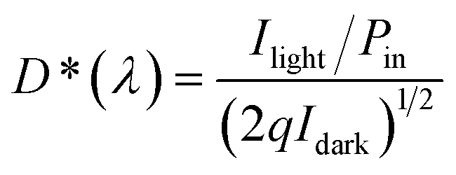
where Ad is the effective area of the device, f is the bandwidth, and In is the noise current. When dark current is predominantly caused by shot noise, the detectivity is given by:| |
 | (2) |
where q is the elementary charge. D* (expressed in Jones), as the most important performance parameter of a photodetector, is used to evaluate the performance of photodetectors with different configurations and sizes. D* is directly proportional to responsivity and indirectly influenced by parameters such as wavelength, modulation frequency, and electric field.55
3.5 External quantum efficiency (EQE)
EQE refers to the ratio of the number of electrons collected by a photodetector (i.e., conversion of light to photocurrent) to the number of incident photons. In general, EQE is given by:| |
 | (3) |
where e is the elementary charge, R is the responsivity, h is the Planck constant, ν and λ are the frequency and wavelength of the incident light, and c is the speed of light.
4. Design of graphitic carbon nitride photodetectors and the performance regulation strategies
Generally, g-C3N4 derived by thermal condensation method is powder material with a bulk structure, smaller surface area, lower crystallinity degree and abundant lattice defects. This type of g-C3N4 is not desired and not very suitable for photodetectors, due to the lower intrinsic conductivity and rapid recombination of photogenerated charge carriers. To effectively enhance the performance of g-C3N4, researchers recently have adopted various methodologies including atomic doping, heterostructure, composite design and controllable growth of high-quality film which will be introduced as follows.
4.1 Atomic doping and defect control
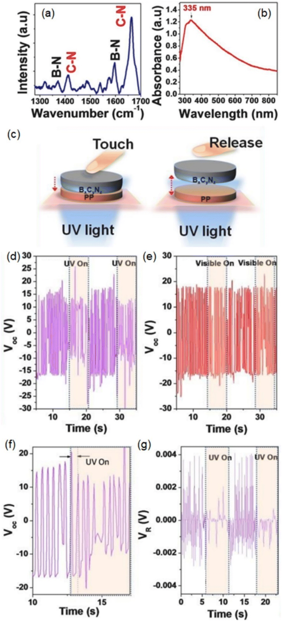
Atomic doping and defect engineering can directly influence the local electronic structure of g-C3N4, thereby altering the energy level positions and achieving enhanced light response and improved charge carrier separation efficiency. Goswami et al. utilized hydrogen atom filling in the nitrogen vacancies of g-C3N4 (H–g-C3N4) to modulate its optoelectronic properties.64 After hydrogen atom filling, the H–g-C3N4 exhibits a significant redshift in optical absorption spectrum, extending from the visible light range to the near-infrared region, with a narrow band gap of only 2.06 eV and a significant decrease in fluorescence intensity. Owing to effective charge carrier separation and enhanced light absorption at interfacial defects, the photodetector based on H–g-C3N4/p-type silicon demonstrates excellent performance in a wide spectral range of 350 to 1100 nm: responsivity of 0.34 A W−1, external quantum efficiency of 59%, and an on/off ratio greater than 1000. Ray et al. synthesized boron-doped g-C3N4 (BxCyNz) nanosheets with enhanced UV absorption and extended visible-light absorption edge (Fig. 2b).63 The local nitrogen atom deficiency in the structure can form trap centers that facilitate the separation of photo-generated electron–hole pairs. Subsequently, a single-electrode triboelectric nanogenerator (STENG) based on BxCyNz nanosheets was fabricated and used for wearable UV photodetection. By assembling BxCyNz and polypropylene (PP), UV light is irradiated through PP onto the BxCyNz layer (Fig. 2c), and the variation in open-circuit voltage is achieved under both UV-illuminated and non-illuminated conditions through continuous switching between touch and non-touch modes (Fig. 2d and e). When the light power increases to 1.5 mW cm−2, the output voltage decreases from 20.3 V to 12.9 V, with a response time of less than 5 s (Fig. 2f). The closed-circuit voltage connected to the load decreases to approximately 60% of the value without light illumination (Fig. 2g). Under UV light irradiation, BxCyNz generates photo-generated electron–hole pairs that migrate to the top and bottom, creating opposite electric fields, which reduce the friction charge and result in a decrease in the potential and open-circuit voltage of the STENG.
 |
| | Fig. 2 (a) Raman spectrum (λ = 785 nm) and (b) UV-vis absorption spectrum of the BxCyNz (x![[thin space (1/6-em)]](https://www.rsc.org/images/entities/char_2009.gif) :y:z = 0.676:0.181:0.143 after normalizing the atomic percentages) nanosheet at room temperature. (c) Schematic illustration of UV photodetection of the BxCyNz/PP STENG under touch-release action. (d) The change of open circuit voltage (VOC) with UV exposure during continuous touch-release action. (e) The change of VOC under visible light with same bio-mechanical motion. (f) Response and (g) closed circuit voltage (VR) of STENG under UV radiation. Reprinted from ref. 63 with permission. Copyright 2023, Elsevier. :y:z = 0.676:0.181:0.143 after normalizing the atomic percentages) nanosheet at room temperature. (c) Schematic illustration of UV photodetection of the BxCyNz/PP STENG under touch-release action. (d) The change of open circuit voltage (VOC) with UV exposure during continuous touch-release action. (e) The change of VOC under visible light with same bio-mechanical motion. (f) Response and (g) closed circuit voltage (VR) of STENG under UV radiation. Reprinted from ref. 63 with permission. Copyright 2023, Elsevier. | |
4.2 Heterostructure
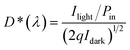
Constructing heterostructure is the most commonly used strategy for designing g-C3N4 based photodetectors.65–76 Shan et al. fabricated high-quality g-C3N4 films on Si substrate using a vapor-phase transport-assisted condensation method.65 The g-C3N4/Si heterostructure exhibited a distinct response under the light irradiation from 300 to 1000 nm with a responsibility of 133 A W−1 and detectivity of 3.3 × 10¹² Jones (Fig. 3a and b). When exposed to light irradiation, the τrise and τfall were 28 and 70 μs, respectively (Fig. 3c). A position-sensitive detector based on the g-C3N4/Si heterojunction showed a superior nonlinearity of 0.9% and the maximum sensitivity was 352 mV mm−1 at 808 nm (Fig. 3d and e). According to the energy level diagram, a type-I heterojunction can be formed between g-C3N4 and Si since the Fermi level of g-C3N4 is higher than that of Si (Fig. 3g). Under the light irradiation, the photogenerated electrons migrate to g-C3N4 while the holes are accumulated on the Si side (Fig. 3h), which can be used for self-powered photodetectors after connecting to the positive and negative terminals of external circuit. When the laser spot was incident on the PSD, the separation of photogenerated carriers by the built-in field left a gradient of charge carriers between the illuminated and non-illuminated parts. Once the excessive electrons in the illuminated area moved to the electrode, a lateral photovoltaic voltage was created to achieve the PDS function (Fig. 3i). In addition, they replaced the silicon with GaN and also found a built-in electric field in g-C3N4/GaN heterostructure,75 of which the sensitivity was up to 355 mV mm−1 and the nonlinear value of 0.5% at room temperature. When the temperature was elevated to 700 K, the sensitivity (315 mV mm−1) and nonlinear value (1.4%) were still superior to the commercial Si devices.
 |
| | Fig. 3 (a) Responsivity and (b) detectivity of g-C3N4/Si photodetector under light irradiation with different wavelengths. (c) Response speed of g-C3N4/Si photodetector. (d) Schematic illustration of g-C3N4/Si position-sensitive detector (PSD). (e) Light spot position dependent lateral photovoltage. (f) Sensitivity of g-C3N4/Si PSD as a function of light power. Schematic illustration of (g) energy levels of g-C3N4 and Si, (h) energy band of g-C3N4/Si heterojunction under illumination at 0 V bias, (i) the lateral diffusion flow of the electrons photoexcited in Si away from laser spot in the inversion layer at the g-C3N4/Si interface. Reproduced from ref. 65 with permission. Copyright 2023, Springer. | |
Alshareef et al. utilized a low-temperature solution processing method to fabricate a type-II heterojunction consisting of P-doped g-C3N4 (PCN-S) nanosheets and CH3NH3PbClxI3−x (MLHP) perovskite.70 Since the dark current decreased by two orders of magnitude, the on/off ratio of the device reached up to 105 (Fig. 4a), with a responsivity of 1.7 A W−1 and a detectivity of 1.1 × 10¹² Jones (Fig. 4b). When a heterojunction formed between PCN-S and MLHP, the interfacial band bending took place to form a barrier, hindering the electron transfer from MLHP to PCN-S (Fig. 4c). Under light illumination, the photo-generated carriers in MLHP can reduce the built-in electric field and lead to a upshift of Fermi level. As a result, the decreased barrier between conduction bands of PCN-S and MLHP promoted the electron transfer from MLHP to PCN-S and thereby enhanced the photocurrent (Fig. 4d). In addition, the PCN-S/MLHP photodetector exhibited excellent moisture resistance owing to the improved hydrophobicity. Zhang et al. constructed a type-II van der Waals heterojunction by combining Bi zero-dimensional (0D) quantum dots (QDs) and g-C3N4 nanosheets.72 The photodetection performances were studied via photoelectrochemical testing. After forming a heterojunction between Bi QDs and g-C3N4, the redistribution of intrinsic charge carriers resulted in the formation of a depletion region at the interface. Under illumination, photo-generated electrons and holes diffused in opposite directions. As the conduction band (CB) position of g-C3N4 is lower than that of Bi QDs, photo-generated electrons transferred from the CB of Bi QDs to the CB of g-C3N4, while photo-generated holes moved from the valence band (VB) of g-C3N4 to the VB of Bi QDs, thereby creating a built-in electric field. The presence of the built-in electric field effectively promoted the separation of photo-generated carriers and improved the light response capability.
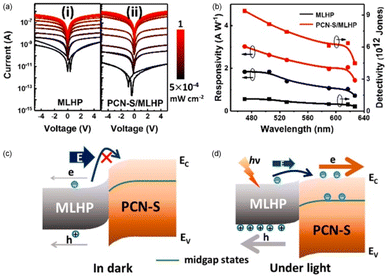 |
| | Fig. 4 (a) I–V curves of (i) MLHP-only and (ii) PCN-S/MLHP hybrid photodetectors measured in the dark and under various wight light irradiation. (b) Calculated responsivity and detectivity under a bias of 5 V as a function of wavelength. Schematic illustration of band diagram at the MLHP/PCN-S interface in (c) dark and (d) illuminated conditions. Reprinted from ref. 70 with permission. Copyright 2019, American Chemical Society. | |
4.3 Composite design
Alshareef et al. first exfoliated bulk g-C3N4 and MoS2 into nanosheets, and then mixed them to form an inorganic–organic thin-film composite (Fig. 5a), which was used for the fabrication of planar photodetectors.77 With the decreasing content of g-C3N4, the absorption of the composite material towards UV light gradually weakened, while its visible light absorption capability increased (Fig. 5b). When the two components were present in equal proportions, the photodetectors exhibited the highest on/off ratio under 532 nm and 365 nm wavelength illuminations (Fig. 5c), with maximum responsivity and specific detectivity values of 4 A W−1 and 4 × 10¹¹ Jones, respectively (wavelength: 365 nm, light power: 0.5 W cm−2). Femtosecond transient absorption spectra confirmed that the composite material possessed faster photogenerated charge carrier transfer dynamics, which was the main reason for the increase in photocurrent. Furthermore, the thin-film composite photodetectors also exhibited outstanding mechanical performance, as the on/off ratio did not show significant degradation even after bending at different degrees and multiple bending tests (Fig. 5d and e). Zhao et al. used g-C3N4 quantum dots to modify the interface of tin oxide/perovskite.78 It was found that the g-C3N4 quantum dots were able to improve the crystallinity of the perovskite layer, reduce grain boundaries and defects, and suppress the recombination of photogenerated charge carriers. After the modification with g-C3N4 quantum dots, both the responsivity and on/off ratio of the photodetectors were greatly enhanced.
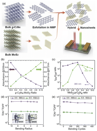 |
| | Fig. 5 (a) Schematic illustration of the process for preparation of g-C3N4 and MoS2 hybrid dispersions used for photodetector; (b) absorbance at wavelengths of 672 and 308 nm and (c) on–off ratio as a function of the g-C3N4 and MoS2 ratio. (d) On–off ratio of the photodetectors containing g-C3N4 and MoS2 hybrid with different bending radius. (e) On–off ratio of the photodetectors containing g-C3N4 and MoS2 hybrid with different bending cycles at a banding radius of ≈4 mm. Reproduced from ref. 77 with permission. Copyright 2017, John Wiley and Sons Ltd. | |
4.4 Controllable fabrication of high-quality films
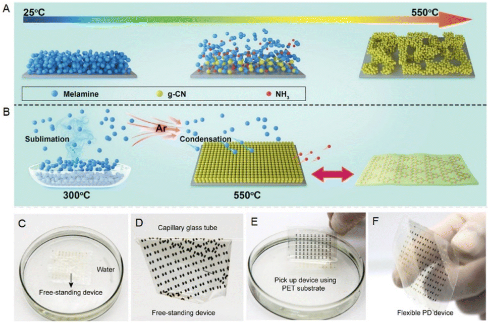
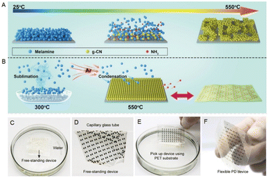
As introduced above, the g-C3N4 bulk powder prepared by conventional methods is not high desired and still needs to be post-treated through secondary exfoliation before being coated onto substrate surfaces to fabricate thin film devices. Although small-sized and ultra-thin g-C3N4 nanosheets can be further processed into micro–nano devices, the existing processes for preparing g-C3N4 films still have significant limitations in manufacturing large-sized optoelectronic devices at the wafer level. Moreover, the overall device performances are strongly dependent on the structural defects, surface roughness, and weak bonding between the thin film and substrate resulting from multiple material processing steps. Shan et al. proposed a vapor transport-assisted condensation (VTC) synthesis method, which achieved controllable preparation of wafer-sized g-C3N4 films.79 In the traditional direct thermal polymerization method, a large number of holes exist in the products due to the sublimation and low migration rate of the melamine precursor during the pyrolysis process, making it difficult to obtain uniform high-quality films (Fig. 6A). Using the VTC method, melamine and the substrate were placed in the low-temperature (300 °C) and high-temperature (550 °C) region respectively. The appropriate amount of gaseous melamine formed in the low-temperature region can uniformly transport to the substrate surface to complete the polymerization process (Fig. 6B). In addition, the hydrogen bonding interaction between the terminal –NH groups of the g-C3N4 structure and water molecules leads to the formation of wrinkles on the film surface, which can be peeled off from the quartz substrate surface and then float on the water. Then, the peeled g-C3N4 was transferred onto a polyethylene terephthalate (PET) flexible substrate through a glass capillary (Fig. 6C–F). The responsivity of the flexible g-C3N4 UV photodetector array was 207 mA W−1, with a switch ratio of 250 and a response time of 6 ms. Liang et al. obtained high-quality g-C3N4 films using a laser direct writing (LDW) technology. They coated a mixture of pre-calcinated precursor powder, carbon black, and ethylene glycol onto a conductive glass surface and then irradiated the glass backside with a near-infrared laser at a wavelength of 1064 nm. The instantaneous high temperature and pressure generated by the laser enable the completion of the copolymerization reaction within only 4 s.80 The photodetector (with 36 pixels) prepared by LDW technology not only exhibits excellent mechanical performance and stability but also has a dark current of only 4.43 × 10⁻¹¹ A, which is beneficial for achieving a high signal-to-noise ratio.
 |
| | Fig. 6 Schematic illustration of growth process of g-C3N4 by (A) the direct thermal condensation method and (B) VTC process. (C–F) The transfer process of the g-C3N4 from the quartz to PET substrate. Reprinted from ref. 79 with permission. Copyright 2021, Cell Press. | |
4.5 Others
Using chemical vapor deposition, Xiao et al. prepared an asymmetric carbon nitride nanotube membrane (ACNNM) in an anodized aluminum oxide template.81 Such ACNNM was used for ion-transport-based self-powered photodetector. Unlike the conventional photodetectors that directly use the separated charge carriers for detection and sensing (Fig. 7a), their ion-type photodetector involves electrolyte and the separated photo-induced charge carriers in the asymmetric nanotube structure can drive ion separation and transport within the nanotube channels, generating an ion current signal (Fig. 7b and c). When exposed to green and blue light, a current is detected without applying bias voltage, indicating that the ACNNM can be used for self-powered photodetectors. Additionally, the responsivity of this photodetector decreases by an order of magnitude with decreasing light power, and the response time was 0.05 s. Although the photodetection performance is slightly inferior to that of traditional photodetectors, the carbon nitride ion-type photodetector still exhibits excellent biocompatibility and structural flexibility, which are very important in the field of bioelectronics. Palanisamy et al. transferred g-C3N4 thin film onto the surface of single-layer graphene field-effect transistor (FET) as the UV photodetector.84 The light response is dependent on the g-C3N4 thin film, achieving an on/off ratio of 157 and responsivity was up to 3 × 10³ A W−1. Shan et al. investigated the photodetection characteristics of g-C3N4 through in situ pressure-dependent electrical test.82 The photocurrent of g-C3N4 increased nearly twofold when a pressure of 3.6 GPa was applied (Fig. 7d and e). Such photocurrent increase can be attributed to the enhanced interlayer interactions resulting from a smaller bandgap of g-C3N4 after applying pressure since the electrons were more easily excited from the valence band to the conduction band. Ding et al. revealed that introducing nitrogen defects in g-C3N4 can reduce the bandgap to 2.4 eV.83 When applying the external pressure, the bandgap is further reduced to 1.7 eV, which is the lowest value reported in the literature for g-C3N4. Upon the pressure applied, the photocurrent of g-C3N4 can increase by approximately 50% while bandgap recovers to 1.87 eV when the pressure is released. In situ synchrotron X-ray diffraction and Raman spectroscopy further confirm that the changes in the bandgap originate from pressure-induced and nitrogen vacancy-induced amorphization effects. In addition, the performance of graphitic carbon nitride based photodetectors have been summarized in Table 2.
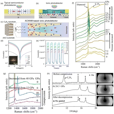 |
| | Fig. 7 Schematic illustration of (a) the typical electron-transport-based photodetector and (b) ion-transport-based photodetector. (c) Schematic illustration of the asymmetric carbon nitride nanotube membrane and the mechanism of light-induced ion transport. Reproduced from ref. 81. Copyright 2019, John Wiley and Sons Ltd. (d) I–V curves of the g-C3N4 photodetector during compression in the dark and under 355 nm laser illumination. (e) Pressure-dependent photocurrent responses of the g-C3N4 photodetector with the illumination turned on and off periodically. Reproduced from ref. 82 with permission. Copyright 2022, Elsevier. (f) Raman spectra of nitrogen-deficient g-C3N4 at high pressures when compression pressure was applied (from 0 to 47.6 GPa) and when pressure was released (from 41.1 to 0.3 GPa). (g) Raman spectra of nitrogen-deficient g-C3N4 at selected pressures. (h) Integrated synchrotron X-ray diffraction patterns and the corresponding two-dimensional XRD patterns. Reproduced from ref. 83 with permission. Copyright 2023, American Physical Society. | |
Table 2 Performance comparison of the reported g-C3N4 based photodetectors
| Materials |
Response time (ms) |
On–off ratio |
Responsivity (A W−1) |
Specific detectivity (Jones) |
External quantum efficiency (%) |
Ref. |
| BxCyNz |
<90 |
— |
∼1.6 × 10³ (V W−1) |
— |
— |
63 |
| H–g-C3N4/p-Si |
180/290 |
— |
0.34 |
1.5 × 10¹¹ |
— |
64 |
| g-C3N4/Si |
0.0031/0.05 |
— |
133 |
3.3 × 10¹² |
— |
65 |
| g-C3N4/graphene |
— |
— |
4 × 10³ |
— |
— |
66 |
| g-C3N4/Si |
0.23/0.60 |
∼1.2 × 10⁵ |
1.2 |
2.8 × 10¹⁴ |
213 |
67 |
| Au–g-C3N4/CdS/ZnO |
— |
∼102 |
— |
— |
— |
68 |
| g-C3N4/N-doped graphene |
— |
— |
5.9 × 10⁻⁴ |
— |
— |
69 |
| PCN-S/MLHP |
— |
105 |
1.7 |
1.1 × 10¹³ |
|
70 |
| g-C3N4/CNTs |
— |
— |
0.23 |
— |
— |
71 |
| g-C3N4@Bi |
— |
— |
2.843 × 10⁻³ |
2.25 × 10¹¹ |
|
72 |
| g-C3N4/GaN |
— |
— |
3 |
∼104 |
103 |
73 |
| g-C3N4/GaN |
— |
— |
0.02 |
5.16 × 10¹² |
— |
74 |
| g-C3N4/GaN |
1.7/2.3 |
2 × 10³ |
0.068 |
— |
— |
75 |
| g-C3N4/MoS2 |
50/80 |
1 × 10⁴ |
4 |
4 × 10¹¹ |
|
77 |
| g-C3N4 film |
6 |
250 |
0.207 |
— |
— |
79 |
| g-C3N4 film |
— |
— |
5 × 10⁻⁵ |
∼1.05 × 10⁶ |
∼1.75 × 10⁻² |
82 |
| CNTF/GFET |
500/2000 |
— |
3 × 10³ |
— |
— |
84 |
5. Conclusion and future perspectives
The structural design, fabrication processes, and performance optimization of g-C3N4-based photodetectors have emerged as a new hotspot in the research field of semiconductor materials. They provide new research directions for the development of novel optoelectronic devices. This review summarizes the recent progress in g-C3N4-based photodetectors and in particular discusses the research strategies for device fabrication and performance optimization. The enhancement in detection performances of g-C3N4-based photodetectors have been achieved by integrating with various semiconductor materials such as oxides, perovskites and quantum dots.
Since the core component of g-C3N4-based photodetectors is the thin-film material, the density, uniformity and defect content of the thin films therefore directly affect the device performance. Despite researchers' efforts to enhance the quality of g-C3N4 films through various novel fabrication methods, there are still challenges in achieving wafer-scale, high polymerization/crystallinity, and low-defect g-C3N4 films for photodetectors with higher responsivity and larger gain. In the future, the development of g-C3N4 photodetectors can focus on the following aspects:
(i) Given that the transport kinetics of photogenerated charge carriers are affected by the low intrinsic conductivity of g-C3N4, how to simply prepare high-quality thin films will play a critical role in achieving practical application of g-C3N4 based photodetectors. Due to the fact that the precursors used for g-C3N4 synthesis are organic small molecules, conventional physical fabrication methods such as molecular beam epitaxy, magnetron sputtering, and pulsed laser deposition are not highly suitable. Therefore, it is crucial to further improve the current chemical vapor deposition (CVD) techniques to accelerate molecular interactions, reduce precursor volatilization, and enhance the copolymerization degree. This will enable the production of high-quality films with high crystallinity and good adhesion to substrates, which are the key factors for g-C3N4 photodetectors.
(ii) The currently reported g-C3N4 optoelectronic devices are mainly used for UV light detection. In the future, much efforts can be devoted to enhance the light-responsive performance of g-C3N4 in the visible and even near-infrared (NIR) regions through compositional modification and structural regulation. On the one hand, introducing the NIR-responsive plasmon metals (such as Au and Ag) is able to enhance the light harvesting owing to the surface plasmon resonance (SPR) effect. On the other hand, compared to planar and symmetric structure, forming highly disordered structure can effectively achieve the n → π* electron transition, thereby further extending the light absorption range. These strategies open up possibilities for the applications of g-C3N4 photodetectors across the entire spectrum.
(iii) To more effectively enhance the detection performance of the current devices, it is worth exploring the heterostructures with emerging materials such as 2D transition metal sulfides/selenides, black phosphorus, MXenes, etc. In particular, the formation of van der Waals heterostructures can not only broaden the wavelength range of photodetection but also significantly improve the response speed and detection sensitivity of the devices.
(iv) Compared to semiconductors like Si and GaAs, g-C3N4 is a polymer material with relatively good mechanical properties. The synthesis of g-C3N4 typically requires high-temperature polymerization while flexible substrates normally cannot be used at such high temperature. Therefore, developing various techniques to transfer high-quality films onto flexible polymer substrates while ensuring an outstanding film-substrate adhesion is highly desired. This enables the realization of flexible photodetectors used in display devices, wearable devices, smart robots, and other fields.
Conflicts of interest
There are no conflicts to declare.
Acknowledgements
This work is financially supported by the Anhui Provincial Natural Science Foundation (1908085QB83), the Guidance Project of Scientific Research Program of Hubei Provincial Department of Education (B2022620), and the Special Research Team Project of Hubei Science and Technology College (Xj2022z01).
References
- M. Tanzid, A. Ahmadivand, R. Zhang, B. Cerjan, A. Sobhani, S. Yazdi, P. Nordlander and N. J. Halas, ACS Photonics, 2018, 5, 3472–3477 CrossRef CAS.
- M. Jin, Y. Wang, M. Chai, C. Chen, Z. Zhao and T. He, Adv. Funct. Mater., 2022, 32, 2107499–2107518 CrossRef CAS.
- P. Liu, S.-E. Yang, Y. Chen, Y. Ma, S. Liu, X. Fang, F. Fan and J. Han, Ceram. Int., 2020, 46, 19655–19663 CrossRef CAS.
- F. H. L. Koppens, T. Mueller, P. Avouris, A. C. Ferrari, M. S. Vitiello and M. Polini, Nat. Nanotechnol., 2014, 9, 780–793 CrossRef CAS PubMed.
- M. A. Iqbal, N. Anwar, M. Malik, M. Al-Bahrani, M. R. Islam, J. R. Choi, P. V. Pham and X. Liu, Adv. Mater. Interfaces, 2023, 10, 2202208 CrossRef CAS.
- G. Konstantatos, Nat. Commun., 2018, 9, 5266 CrossRef CAS PubMed.
- H. Wang, Z. Li, D. Li, P. Chen, L. Pi, X. Zhou and T. Zhai, Adv. Funct. Mater., 2021, 31, 2103106 CrossRef CAS.
- T. Dong, J. Simões and Z. Yang, Adv. Mater. Interfaces, 2020, 7, 1901657 CrossRef CAS.
- H.-P. Wang, S. Li, X. Liu, Z. Shi, X. Fang and J.-H. He, Adv. Mater., 2021, 33, 2003309 CrossRef CAS PubMed.
- Y. Zhang, Y. Ma, Y. Wang, X. Zhang, C. Zuo, L. Shen and L. Ding, Adv. Mater., 2021, 33, 2006691 CrossRef CAS PubMed.
- F. Wang, X. Zou, M. Xu, H. Wang, H. Wang, H. Guo, J. Guo, P. Wang, M. Peng, Z. Wang, Y. Wang, J. Miao, F. Chen, J. Wang, X. Chen, A. Pan, C. Shan, L. Liao and W. Hu, Adv. Sci., 2021, 8, 2100569 CrossRef CAS PubMed.
- J. Xu, W. Zheng and F. Huang, J. Mater. Chem. C, 2019, 7, 8753–8770 RSC.
- A. V. Barve, S. J. Lee, S. K. Noh and S. Krishna, Laser Photonics Rev., 2010, 4, 738–750 CrossRef CAS.
- R. Guo, M. Zhang, J. Ding, A. Liu, F. Huang and M. Sheng, J. Mater. Chem. C, 2022, 10, 7404–7422 RSC.
- D. Yang and D. Ma, Adv. Opt. Mater., 2019, 7, 1800522 CrossRef.
- M. Chen, C. Wang and W. Hu, J. Mater. Chem. C, 2021, 9, 4709–4729 RSC.
- X. Wang, K. Maeda, A. Thomas, K. Takanabe, G. Xin, J. M. Carlsson, K. Domen and M. Antonietti, Nat. Mater., 2009, 8, 76–80 CrossRef CAS PubMed.
- W.-J. Ong, L.-L. Tan, Y. H. Ng, S.-T. Yong and S.-P. Chai, Chem. Rev., 2016, 116, 7159–7329 CrossRef CAS PubMed.
- F. K. Kessler, Y. Zheng, D. Schwarz, C. Merschjann, W. Schnick, X. Wang and M. J. Bojdys, Nat. Rev. Mater., 2017, 2, 17030–17046 CrossRef CAS.
- G. Liao, F. He, Q. Li, L. Zhong, R. Zhao, H. Che, H. Gao and B. Fang, Prog. Mater. Sci., 2020, 112, 100666–100686 CrossRef CAS.
- Y. Dong, Q. Wang, H. Wu, Y. Chen, C.-H. Lu, Y. Chi and H.-H. Yang, Small, 2016, 12, 5376–5393 CrossRef CAS PubMed.
- H. Y. Hoh, Y. Zhang, Y. L. Zhong and Q. Bao, Adv. Opt. Mater., 2021, 9, 2100146 CrossRef CAS.
- P. Xia, B. Cheng, J. Jiang and H. Tang, Appl. Surf. Sci., 2019, 487, 335–342 CrossRef CAS.
- J. Liebig, Ann. Pharmacother., 1834, 10, 10–1002 Search PubMed.
- E. C. Franklin, J. Am. Chem. Soc., 1922, 44, 486–509 CrossRef CAS.
- L. Pauling and J. H. Sturdivant, Proc. Natl. Acad. Sci. U.S.A., 1937, 23, 615–620 CrossRef CAS PubMed.
- D. M. Teter and R. J. Hemley, Science, 1996, 271, 53–55 CrossRef CAS.
- E. Kroke, M. Schwarz, E. Horath-Bordon, P. Kroll, B. Noll and A. D. Norman, New J. Chem., 2002, 26, 508–512 RSC.
- F. Fina, S. K. Callear, G. M. Carins and J. T. S. Irvine, Chem. Mater., 2015, 27, 2612–2618 CrossRef CAS.
- X. Ma, Y. Lv, J. Xu, Y. Liu, R. Zhang and Y. Zhu, J. Phys. Chem. C, 2012, 116, 23485–23493 CrossRef CAS.
- Y.-X. Yu, Phys. Chem. Chem. Phys., 2013, 15, 16819–16827 RSC.
- G. Zhang, Z.-A. Lan and X. Wang, Angew. Chem., Int. Ed., 2016, 55, 15712–15727 CrossRef PubMed.
- M. Liu, C. Wei, H. Zhuzhang, J. Zhou, Z. Pan, W. Lin, Z. Yu, G. Zhang and X. Wang, Angew. Chem., Int. Ed., 2022, 61, e202113389 CrossRef CAS PubMed.
- Y. Li, M. Gu, X. Zhang, J. Fan, K. Lv, S. A. C. Carabineiro and F. Dong, Mater. Today, 2020, 41, 270–303 CrossRef CAS.
- M. Casalino, G. Coppola, R. M. De La Rue and D. F. Logan, Laser Photonics Rev., 2016, 10, 895–921 CrossRef CAS.
- Y.-M. Niquet, C. Delerue, D. Rideau and B. Videau, IEEE Trans. Electron Devices, 2012, 59, 1480–1487 CAS.
- H. R. Shanks, P. D. Maycock, P. H. Sidles and G. C. Danielson, Phys. Rev., 1963, 130, 1743–1748 CrossRef CAS.
- M. A. Hopcroft, W. D. Nix and T. W. Kenny, J. Microelectromech. Syst., 2010, 19, 229–238 CAS.
- A. Srivastava, R. Srivastava, J. Wang and J. Kono, Phys. Rev. Lett., 2004, 93, 157401 CrossRef PubMed.
- H. G. B. Hicks and D. F. Manley, Solid State Commun., 1969, 7, 1463–1465 CrossRef CAS.
- A. Amith, I. Kudman and E. F. Steigmeier, Phys. Rev., 1965, 138, A1270–A1276 CrossRef.
- T.-H. Fang, W.-J. Chang and C.-M. Lin, Microelectron. Eng., 2005, 77, 389–398 CrossRef CAS.
- I. Meric, M. Y. Han, A. F. Young, B. Ozyilmaz, P. Kim and K. L. Shepard, Nat. Nanotechnol., 2008, 3, 654–659 CrossRef CAS PubMed.
- K. I. Bolotin, K. J. Sikes, Z. Jiang, M. Klima, G. Fudenberg, J. Hone, P. Kim and H. L. Stormer, Solid State Commun., 2008, 146, 351–355 CrossRef CAS.
- A. A. Balandin, S. Ghosh, W. Bao, I. Calizo, D. Teweldebrhan, F. Miao and C. N. Lau, Nano Lett., 2008, 8, 902–907 CrossRef CAS PubMed.
- J.-U. Lee, D. Yoon and H. Cheong, Nano Lett., 2012, 12, 4444–4448 CrossRef CAS PubMed.
- K. F. Mak, C. Lee, J. Hone, J. Shan and T. F. Heinz, Phys. Rev. Lett., 2010, 105, 136805 CrossRef PubMed.
- R. Fivaz and E. Mooser, Phys. Rev., 1967, 163, 743–755 CrossRef CAS.
- S. Sahoo, A. P. S. Gaur, M. Ahmadi, M. J. F. Guinel and R. S. Katiyar, J. Phys. Chem. C, 2013, 117, 9042–9047 CrossRef CAS.
- S. Bertolazzi, J. Brivio and A. Kis, ACS Nano, 2011, 5, 9703–9709 CrossRef CAS PubMed.
- Z. Pan, M. Liu, G. Zhang, H. Zhuzhang and X. Wang, J. Phys. Chem. C, 2021, 125, 9818–9826 CrossRef CAS.
- G. Yu, K. Gong, C. Xing, L. Hu, H. Huang, L. Gao, D. Wang and X. Li, Chem. Eng. J., 2023, 461, 142140 CrossRef CAS.
- B. Mortazavi, G. Cuniberti and T. Rabczuk, Comput. Mater. Sci., 2015, 99, 285–289 CrossRef CAS.
- L.-W. Ruan, Y.-J. Zhu, L.-G. Qiu, Y.-P. Yuan and Y.-X. Lu, Comput. Mater. Sci., 2014, 91, 258–265 CrossRef CAS.
- R. Saran and R. J. Curry, Nat. Photonics, 2016, 10, 81–92 CrossRef CAS.
- Q. Qiu and Z. Huang, Adv. Mater., 2021, 33, 2008126–2008144 CrossRef CAS PubMed.
- F. Yan, Z. Wei, X. Wei, Q. Lv, W. Zhu and K. Wang, Small Methods, 2018, 2, 1700349 CrossRef.
- F. Teng, K. Hu, W. Ouyang and X. Fang, Adv. Mater., 2018, 30, 1706262 CrossRef PubMed.
- F. Wang, T. Zhang, R. Xie, Z. Wang and W. Hu, Nat. Commun., 2023, 14, 2224 CrossRef CAS PubMed.
- M. Peng, Z. Wen and X. Sun, Adv. Funct. Mater., 2023, 33, 2211548 CrossRef CAS.
- R. C. Jones, Proc. IEEE, 1959, 47, 1495–1502 Search PubMed.
- L. Dou, Y. Yang, J. You, Z. Hong, W.-H. Chang, G. Li and Y. Yang, Nat. Commun., 2014, 5, 5404–5410 CrossRef CAS PubMed.
- S. Bayan, S. Pal and S. K. Ray, Appl. Mater. Today, 2023, 30, 101686 CrossRef.
- A. Ghosh, H. Saini, A. Sarkar, P. Guha, A. K. Samantara, R. Thapa, S. Mandal, A. Mandal, J. N. Behera, S. K. Ray and D. K. Goswami, Appl. Surf. Sci., 2021, 556, 149773 CrossRef CAS.
- X. Chen, X. Yang, Q. Lou, Y. Tian, Z. Liu, C. Lv, Y. Chen, L. Dong and C.-X. Shan, Nano Res., 2023, 16, 1277–1285 CrossRef CAS.
- S. K. Lai, C. Xie, K. S. Teng, Y. Li, F. Tan, F. Yan and S. P. Lau, Adv. Opt. Mater., 2016, 4, 555–561 CrossRef CAS.
- N. Prakash, G. Kumar, M. Singh, A. Barvat, P. Pal, S. P. Singh, H. K. Singh and S. P. Khanna, Adv. Opt. Mater., 2018, 6, 1800191 CrossRef.
- S. Pal, S. Bayan and S. K. Ray, Nanoscale, 2018, 10, 19203–19211 RSC.
- X. Gan, R. Lv, T. Zhang, F. Zhang, M. Terrones and F. Kang, Carbon, 2018, 138, 69–75 CrossRef CAS.
- Z. Liu, Y. Zhu, J. K. El-Demellawi, D. B. Velusamy, A. M. El-Zohry, O. M. Bakr, O. F. Mohammed and H. N. Alshareef, ACS Energy Lett., 2019, 4, 2315–2322 CrossRef CAS.
- H. Fang, H. Ma, C. Zheng, S. Lennon, W. Wu, L. Wu and H. Wang, Appl. Surf. Sci., 2020, 529, 147122 CrossRef CAS.
- Y. Zhang, Y. Xu, J. Guo, X. Zhang, X. Liu, Y. Fu, F. Zhang, C. Ma, Z. Shi, R. Cao and H. Zhang, Chem. Eng. J., 2021, 420, 129556 CrossRef CAS.
- K. Sarkar and P. Kumar, Appl. Surf. Sci., 2021, 566, 150695 CrossRef CAS.
- M. Reddeppa, N. T. KimPhung, G. Murali, K. S. Pasupuleti, B.-G. Park, I. In and M.-D. Kim, Sens. Actuators, B, 2021, 329, 129175 CrossRef CAS.
- X. Chen, D. Yang, X. Yang, Q. Lou, Z. Liu, Y. Chen, C. Lv, L. Dong and C.-X. Shan, Energy Environ. Mater., 2023 DOI:10.1002/eem2.12515.
- M. P. Selvi, N. Shobanadevi and N. Kaliyan, Chem. Pap., 2023, 77, 5409 CrossRef CAS.
- D. B. Velusamy, M. A. Haque, M. R. Parida, F. Zhang, T. Wu, O. F. Mohammed and H. N. Alshareef, Adv. Funct. Mater., 2017, 27, 1605554 CrossRef.
- P. Liu, Y. Sun, S. Wang, H. Zhang, Y. Gong, F. Li, Y. Shi, Y. Du, X. Li, S.-s. Guo, Q. Tai, C. Wang and X.-Z. Zhao, J. Power Sources, 2020, 451, 227825 CrossRef CAS.
- Z. Liu, C. Wang, Z. Zhu, Q. Lou, C. Shen, Y. Chen, J. Sun, Y. Ye, J. Zang, L. Dong and C.-X. Shan, Matter, 2021, 4, 1625–1638 CrossRef CAS.
- H. Tan, W. Si, W. Peng, Y. Wang, D. Liu, L. Wang, C. Jiang, L. Di, J. Liang and F. Hou, Carbon
Energy, 2022, 4, 1228–1241 CrossRef CAS.
- K. Xiao, B. Tu, L. Chen, T. Heil, L. Wen, L. Jiang and M. Antonietti, Angew. Chem., Int. Ed., 2019, 58, 12574–12579 CrossRef CAS PubMed.
- Y. Li, X. Yang, C. Lv, J. Qin, C. Zhang, Z. Zhang, X. Chen, J. Zang, Q. Lou, L. Dong and C.-X. Shan, Carbon, 2022, 199, 453–461 CrossRef CAS.
- P. Cheng, D. Yao, J. Yan, T. Ye, H. Liu, H. Zeng, X. Pan, G. Zhang and J. Ding, Phys. Rev. Appl., 2023, 19, 024048 CrossRef CAS.
- T. Palanisamy, S. Mitra, N. Batra, J. Smajic, A.-H. Emwas, I. Roqan and P. M. F. J. Costa, Adv. Mater. Interfaces, 2022, 9, 2200313 CrossRef CAS.
|
| This journal is © The Royal Society of Chemistry 2023 |
Click here to see how this site uses Cookies. View our privacy policy here. 
 Open Access Article
 This Open Access Article is licensed under a Creative Commons Attribution-Non Commercial 3.0 Unported Licence
 *c
*c