DOI:
10.1039/D3RA03996J
(Paper)
RSC Adv., 2023,
13, 27106-27115
Physical properties of the low-cost CZTS absorber layer deposited by spin-coating: effect of the copper concentration associated with SCAPS-1D simulation
Received
14th June 2023
, Accepted 16th August 2023
First published on 11th September 2023
Abstract
Five samples of copper zinc tin sulfide (CZTS) thin films were deposited by a spin-coating technique at various copper concentrations ranging from 0.5 M to 2.5 M in steps of 0.5 M, in order to improve their stability, efficiency, performance, and reduce the production costs. The XRD patterns showed the existence of the three main characteristic peaks of CZTS (112), (220), and (312), which indicated the formation of the kesterite structure of CZTS. The gap energy of the thin films was calculated based on the derivation method using the absorbance data, and the values obtained varied from 1.46–1.58 eV for 0.5, 1, 1.5, 2, and 2.5 M copper molarity, respectively. Hall effect measurements were used to determine conductivity, which in turn increased with the concentration of copper in the films. The characterization results showed that the sample C3, which represents the 1.5 M copper concentration, exhibited higher crystallinity and better optical and electrical performance than the others. Finally, a theoretical efficiency of 11.6% was obtained when simulating the solar cell using the CZTS thin film (CZTS/ZnS/S:ZnO) in the SCAPS-1D simulation program using the parameters obtained in this study. Under the adopted synthesis conditions, the theoretical simulation corroborated the experimental findings, thus confirming that the synthesized material is a promising candidate for solar cell applications as an absorber layer.
1. Introduction
Nowadays, most companies aim to fabricate photovoltaic (PV) solar cells using ecofriendly and low-cost materials with good efficiencies, but this is a difficult double-edged sword strategy to achieve. Quaternary semiconducting materials based on the kesterite (A2BCX4) mineral structure are good candidates to address this challenge.1,2 Most PV solar cells are manufactured using CdTe or CIGSe materials;3 however, the toxicity of selenium (Se) and the low abundance of indium (In) and gallium (Ga) make the production of CdTe and CIGSe more difficult and hence affect the utility of these low-cost quaternary materials.
Table 1 gives an insight into how much different solar cell types cost, showing that CZTS solar cells, which cost $0.23/W,4 are the most economical, followed by CIGS at $0.30/W,4 monocrystalline silicon, or M–Si, at $0.56/W,5 and cadmium telluride, or CdTe, at $0.84/W.6 When assessing the economic feasibility of various solar cell technologies for different applications, the cost per Watt might be a crucial aspect to take into account.
Table 1 Comparative costs of different solar cells
| CZTS |
0.23$/W |
| CIGS |
0.30$/W |
| M–Si |
0.56$/W |
| CDTe |
0.84$/W |
Copper zinc tin sulfide (CZTS) is a promising absorber material for thin film heterojunction solar cells with optimal solar cell characteristics, such as an ideal band gap (1.4–1.5 eV), high absorption coefficient (104 cm−1), and p-type conductivity.7 Further, this was first deduced from CIGSe by replacing In with Zn, Ga with Sn, and Se with S.8 CZTS is often found in two forms depending on the position of the Cu and Zn atoms: kesterite and stannite.9 Several physical and chemical techniques have been used to synthesize this material, such as electrodeposition,10,11 spray pyrolysis,12 and sputtering deposition.13,14,16 However, only a few studies have been devoted to the deposition of CZTS by spin-coating via a sol–gel method without any sulfurization, which can be classified as a low-cost, simple, non-vacuum, ecofriendly, and suitable large-scale fabrication technique, while additionally having the capacity to generate highly homogenous films rapidly and facilely.
The theoretical efficiency of PV solar cells of CZTS as an absorber material is between 31–33% according to Shockley–Queisser photon-balanced calculations.15 Nevertheless, the experimental efficiency of CZTS lags behind and only increased from 6.7% in 2008 [ref. 13] to 11.1% in 2012 (ref. 17). Wang et al. achieved the highest photovoltaic conversion efficiency of CZTS(Se), which was 12.6%, by exploiting a hydrazine-based approach.18
Recently, there has been great interest in improving the efficiency of CZTS solar cells, Haddout et al. introduced a modeling procedure to predict the effect of each layer of the solar cell, whereupon they found that the CdS layer and the CdS/CZTS interface contribute to the performance degradation.19 On the other hand, by including ZnO/CdS/CZTS in the SCAPS-1D simulation program by optimizing the thickness of each layer and all the electrical parameters, the theoretical efficiency was found to be 14.09%.20
Several studies have reported increases in the efficiency of CZTS recently depending on many parameters, such as solvent, temperature, and elemental concentration, However only few researchers have deployed the use of an initial experimental method in which one of those variable factor have been considered alone in order to enhance the performance of CZTS solar cells.
In previous studies, difficulties were found in obtaining an adequate copper concentration that would lead to a perfect absorber material, although only few researchers investigated the effect of the precursor molarities on the physical properties of CZTS thin films prepared using the sol–gel method, which are well known for their high purity and ability to obtain a final homogeneous structure. Ynineb et al. found that the deposition of CZTS by spray pyrolysis with different concentrations led to a good film with a nearly stoichiometric form and a desirable band gap of 1.51 eV at 0.015 M copper molarity.21 Choudhari et al. found that the Cu-rich structure resulted in disorder in the kesterite structure.22 Moreover, the electrical properties of CZTS are extremely sensitive to the ratio of Cu and Zn in the films.
This work aimed to study the variation in the elemental concentration to obtain a pure kesterite phase and thereby an efficient photovoltaic solar cell. CZTS thin films were synthesized by a spin-coating technique without sulfurization. The effect of the copper concentration on the physical properties was investigated. The solar cell performance was also determined by utilizing the experimental values of the physical properties of CZTS found in this work when applied in a solar cell and inputting them into a solar cell capacitance simulator (SCAPS-1D).23
2. Experimental details
2.1. Chemicals
The precursors used in order to prepare the CZTS thin films here were: copper chloride(II) (CuCl2), zinc chloride(II) (ZnCl2), tin chloride (IV) (SnCl2), and thiourea (SC(NH2)2) as the metal precursors and sources of Cu, Zn, Sn, and S, respectively, with 2-methoxyethanol and MEA (monoethanolamine) used as the solvents. All the chemical grade reagents and solvents were used without further purification.
2.2. Synthesis procedure
CZTS thin films were deposited on soda lime glass substrates using the spin-coating technique, after first being prepared using the sol–gel method, the precursor solution was obtained using metal chloride precursors that were dissolved in 10 mL of 2-methoxyethanol mixed with 10 μL of MEA in the molar ratio of x![[thin space (1/6-em)]](https://www.rsc.org/images/entities/char_2009.gif) :1:1:8 for Cu, Zn, Sn, S, respectively, where x represents the variation of the copper concentration (x = 0.5, 1, 1.5, 2, 2.5 M). The mixture of these elements was stirred for 20 min at 25 °C until obtaining a clear yellow solution. Before deposition, the substrates were cleaned ultrasonically, and soaked in acetone, ethanol, and then distilled water. The solutions were spin-coated at 3000 rpm for 30 s in the air, followed by preannealing on a heating plate at 280 °C, and these steps were repeated twice in order to obtain the desired layer. Fig. 1 presents an overview of the experimental techniques used. Finally, the samples were annealed at 340 °C in the oven for 20 min. The samples were identified as C1, C2, C3, C4, C5, related to the copper concentration varying from 0.5–2.5 M, in steps of 0.5 M.
:1:1:8 for Cu, Zn, Sn, S, respectively, where x represents the variation of the copper concentration (x = 0.5, 1, 1.5, 2, 2.5 M). The mixture of these elements was stirred for 20 min at 25 °C until obtaining a clear yellow solution. Before deposition, the substrates were cleaned ultrasonically, and soaked in acetone, ethanol, and then distilled water. The solutions were spin-coated at 3000 rpm for 30 s in the air, followed by preannealing on a heating plate at 280 °C, and these steps were repeated twice in order to obtain the desired layer. Fig. 1 presents an overview of the experimental techniques used. Finally, the samples were annealed at 340 °C in the oven for 20 min. The samples were identified as C1, C2, C3, C4, C5, related to the copper concentration varying from 0.5–2.5 M, in steps of 0.5 M.
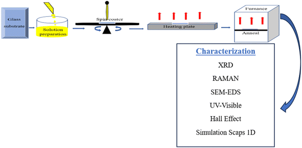 |
| | Fig. 1 Overview of the experimental techniques used. | |
2.3. pH measurement
The pH levels of the solutions were measured and found to be 2.72, 2.58, 2.49, 2.27, and 2.21 for copper concentrations of 0.5, 1, 1.5, 2, and 2.5 M, respectively. It was found that when the copper concentration in the solution was higher, the pH was lower. The stirring temperature (50 °C) could also reduce the pH level, as the temperature and pH are known to be inversely proportional parameters, whereby the vibrations of the molecules in solution increase when increasing the temperature, causing an ionization and the formation of H+ ions. More H+ ions then lead to a more acidic behavior. Several researchers have added different alkaline solutions in order to increase the pH; for instance,24,25 some added a few drops of triethanolamine to the final solution, which had a positive effect on enhancing the crystallinity and the absorbance, which moreover could improve the stability and performance of the high-quality CZTS absorber layer in applications.26
2.4. Experimental methods
The crystalline structure of the films was confirmed by X-ray diffraction (XRD) measurements using a Bragg–Brentano geometry (Bruker D8 Advance), with Cu Kα radiation (λ = 1.5418 Å). Raman spectroscopy was performed to study the phases of the CZTS samples under a laser wavelength of λ = 532 nm in the wavenumber range of 200–500 cm−1. The thin film morphological surface and elemental analysis were examined using field emission scanning electron microscopy (FE-SEM) (JEOL J7600F) and energy-dispersive X-ray spectrometry from a unit attached to the SEM instrument. SEM images were acquired using a fixed electron beam at a low accelerating voltage (10 kV). Optical studies were performed using a computer-controlled ultraviolet-visible-near infrared spectrophotometer (UV-3101PC-SHIMADZU) in the spectral range of 300–1100 nm. Bare glass substrates were used as references for the transmittance measurements. To determine the electrical properties, the resistivity of the samples was measured using the van der Pauw method at room temperature (Ecopia HMS – 5500).
SCAPS is a one-dimensional (1D) solar cell simulation software, developed by several researchers at the Department of Electronics and Information Systems (ELIS) of the University of Gent, Belgium. We performed a numerical simulation of a CZTS solar cell using SCAPS-1D to calculate the theoretical efficiency of the solar cell and output parameters, such as the J–V characteristics.27
3. Results and discussion
3.1. Structural properties
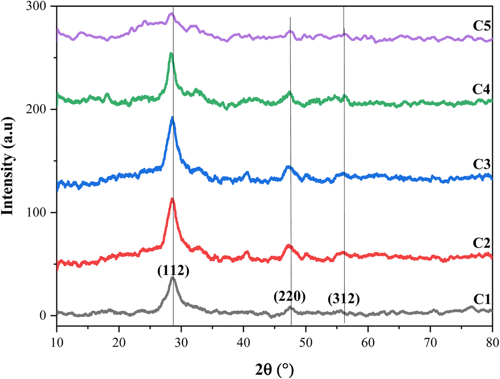
The crystallographic properties of CZTS thin films with different copper molarities were characterized by XRD. Fig. 2 shows three major peaks at Bragg's angles of 2θ = 28.59°, 47.41°, and 56.01°, which were assigned to the lattice planes (112), (220), and (312), respectively. The values above well matched with the standard diffraction data of the Joint Committee on Powder Diffraction Standards (JCPDS) data No. 00-26-0575, and all the thin films crystallized in the kesterite structure. The higher intensity of (112) in all the samples improved the kesterite structure of the CZTS thin films and indicates a preferential orientation along the (112) direction. In addition, the XRD spectra showed a high dependency on the molarity of copper, and the intensity of the (112) peaks increased until 1.5 M copper molarity. However, the intensity of the XRD peak decreased beyond 1.5 M, and when the copper concentration was 2.5 M, the spectrum exhibited some weak peaks. Therefore, a higher concentration of copper includes the appearance of other phases rather than just the pure kesterite one,22 and this can provide Cu-rich conditions in the films that have an enhanced negative effect on the growth of the cell. Ahmed et al. attributed the appearance of secondary phases to the ambient oxygen, which combines with elements in the material to form oxide phases.27
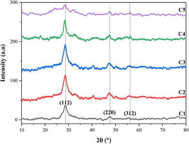 |
| | Fig. 2 X-ray diffraction spectra of the CZTS thin films prepared at different copper concentrations for samples: C1, C2, C3, C4, and C5. | |
The average crystallite size (D) was determined from Scherrer's formula:28
| |
 | (1) |
where
λ is the wavelength of the X-ray diffractometer,
θ is the Bragg diffraction angle,
β is the full width at half maximum (FWHM), and
K is the Scherrer constant, which has a value of 0.9.
Table 2 shows that as the copper concentration increased, the growth of the crystallite size varied from 4.21 nm to 8.34 nm, which was in agreement with the literature.
26,29 The crystallite size values showed that all the films were composed of nano-sized CZTS crystals, and the maximum crystallite size was obtained for sample C4 synthesized with a 2 M copper concentration.
Table 2 Crystalline size, microstress, and dislocation density of CZTS thin films prepared at different copper concentrations: C1 = 0.5 M, C2 = 1 M, C3 = 1.5 M, C4 = 2 M, and C5 = 2.5 M
| Samples |
FWHM (β) |
Crystallite size (nm) |
Dislocation 102 |
Microstrain 103 |
| C1 |
2.04 |
4.21 |
5.64 |
8.15 |
| C2 |
1.36 |
6.3 |
2.45 |
5.43 |
| C3 |
1.34 |
6.47 |
2.38 |
5.35 |
| C4 |
1.04 |
8.34 |
1.43 |
4.15 |
| C5 |
8.5 |
1.02 |
95.97 |
33.95 |
The dislocation density ρ is the number of dislocations per unit volume, which was calculated using the following equation:
| |
 | (2) |
where
D is the crystallite size of the CZTS thin films obtained at different copper concentrations. Stress is an unfavorable factor that can affect the structural properties and source microstrains in the films.
21 The microstrains
ε were thus determined using the following relation:
| |
 | (3) |
where
β is the full width at half maximum (FWHM) and
θ is the Bragg angle. The values of the microstrain and dislocation density (
ε,
ρ) varied along with the copper molarities, and these parameters are presented in
Table 2. Sample C4 showed the greatest crystalline size (
D = 8.34 nm), with the minimum dislocation density and minimum microstrain. Thus, these observations suggest that the optimal molarity of copper is 1.5 M for enhanced crystallographic and microstructural properties.
3.2. Raman spectroscopy
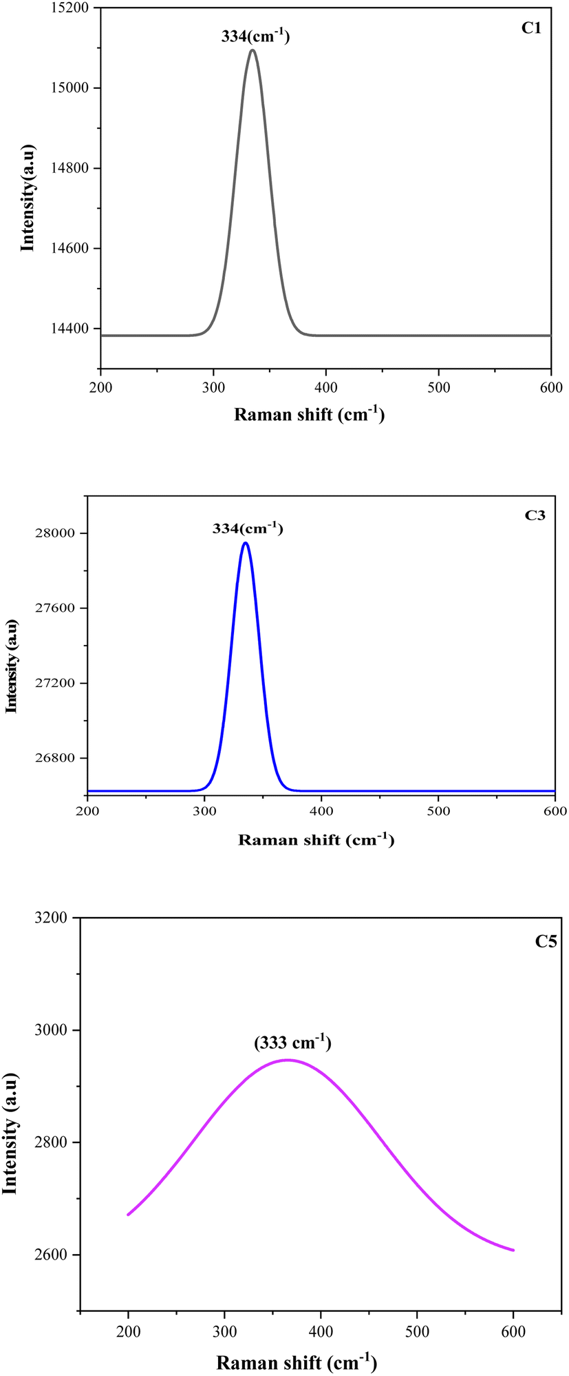
Raman spectroscopy was performed to accomplish the XRD analysis, thus, confirming the crystalline structure and phase formation of the films. Fig. 3 shows the Raman spectra of the CZTS thin films prepared with different copper concentrations. All the spectra exhibited only one single and specific peak position in the Raman scattering in the range of 329–338 cm−1. These values were close to the characteristic peak for CZTS thin films.30,31 Furthermore, the absence of impurity peaks and secondary phases in the prepared samples resulted in the evolution of pure and high-quality CZTS thin films. These results were in good agreement with the XRD analysis and confirmed the presence of phase-pure kesterite CZTS in the spin-coated samples. A higher concentration of copper lead to an increased crystallinity as studied in the XRD part, and, consequently, a lack of secondary phases being observed in the Raman analysis. In addition, the peak observed at 333 cm−1 related to C5 = 2.5 M was very weak and shifted toward the left compared to the others, which was due to the excess Cu concentration in the sample. In fact, there are other factors that could contribute to the peak shift, such as the phonons, non-homogeneity of the size distribution, confinement, strain defects, and non-stoichiometry during film preparation.32
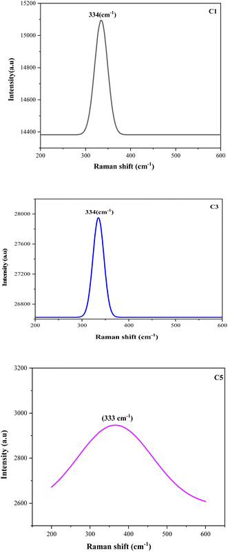 |
| | Fig. 3 Raman spectra of the CZTS thin films prepared at different copper concentrations for samples: C1, C3, and C5. | |
3.3. Morphological and elemental characterization
The surface morphology and elemental composition of the CZTS thin films were investigated by scanning electron microscopy coupled with energy-dispersive X-ray spectroscopy (SEM-EDS). The SEM micrographs presented in Fig. 4 were clearly affected by the variation in copper molarity and revealed that the surface of the films formed a uniform and dense layer. In contrast, sample C5 (Fig. 4E) presented cracks and voids, indicating a degradation of the crystallinity of the film. The cross-sections for all five samples indicated that the film thickness increased with the increase in copper concentration. The thickness size was found as: 1.67, 1.89, 2.12, 2.18, and 3.78 μm for the 0.5, 1, 1.5, 2, and 2.5 M prepared films, respectively. A clear interface with no voids or cavities between the substrate and the film were observed, indicating the growth of a uniform and continuous layer. Higher copper concentrations tended to promote greater grain growth, resulting in an increase in the grain size, as found in the XRD analysis, whereby the crystallite size increased with the copper concentration. Fig. 4 demonstrates that more agglomerated and grouped grains were essentially concentrated when the molarity of copper was higher and reaching the concentration of 2 M; however, for the C5 sample, the presence of voids or pores in the material was noticeable, which could affect the electrical and optical properties of the absorbent layer. The increase in the film thickness might be due to the agglomeration of grains when the concentration of copper was increased because of the high surface energy.33 In addition, Jain et al. found that when the film was Cu rich, the distribution of grains was more uniform, leading to a compact form with fewer cracks.35
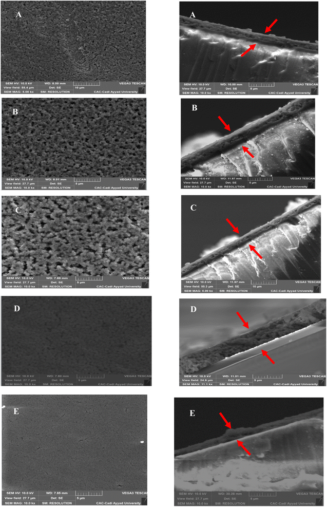 |
| | Fig. 4 SEM images. (A), (B), (C), (D), and (E) surface morphology of the samples C1, C2, C3, C4, and C5 respectively, and cross-sections of C1, C2, C3, C4, and C5, respectively, shown to visualize the thickness of the films prepared. | |
The EDX results are listed in Table 3 and show that all the samples contained the principal elements of CZTS (Cu, Zn, Sn, and S) with different atomic compositions, which were similar to the stoichiometric form. The presence of oxygen and silicon was attributed to the composition of the glass substrate.
Table 3 EDS results for the CZTS thin films for samples C1, C2, C3, C4, and C5
| % Atomic |
C1 |
C2 |
C3 |
C4 |
C5 |
| Cu |
6.37 |
8.80 |
10.55 |
15.91 |
14.84 |
| Zn |
13.09 |
9.58 |
9.27 |
7.88 |
6.37 |
| Sn |
10.89 |
12.72 |
10.08 |
8.88 |
5.20 |
| S |
32.85 |
31.63 |
24.47 |
18.60 |
6.11 |
| Si |
0.52 |
0.2 |
0.83 |
0.45 |
1.62 |
| C |
25.94 |
24.72 |
26.35 |
20.74 |
17.19 |
| Cl |
3.06 |
3.53 |
3.54 |
4.40 |
2.52 |
| O |
7.27 |
9.02 |
14.92 |
23.15 |
46.15 |
3.4. Optical properties
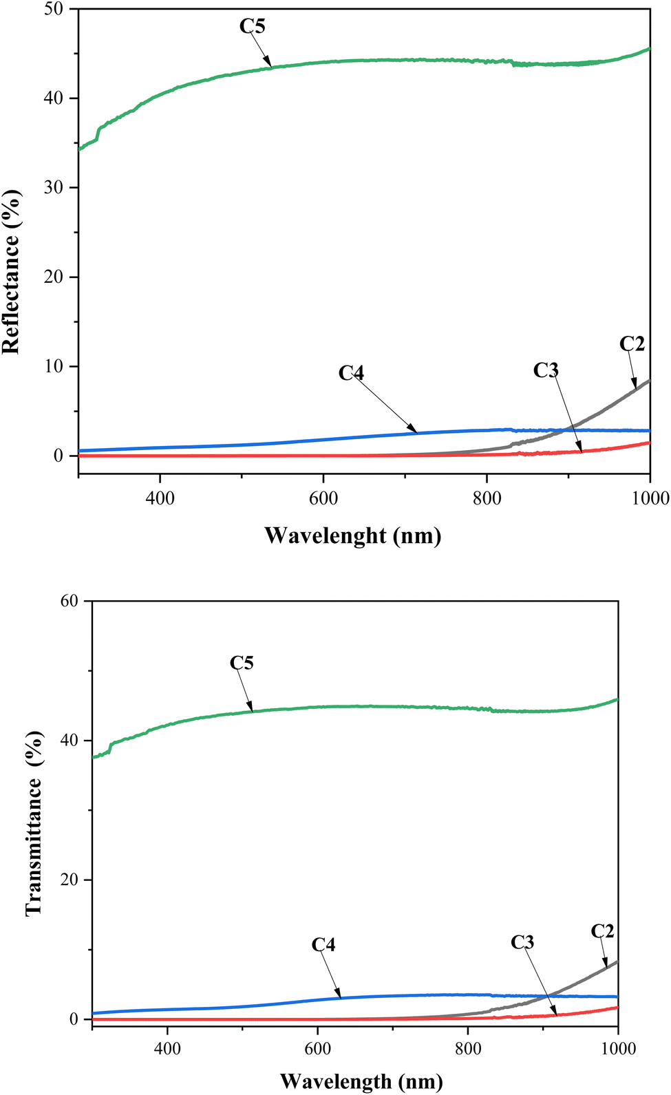
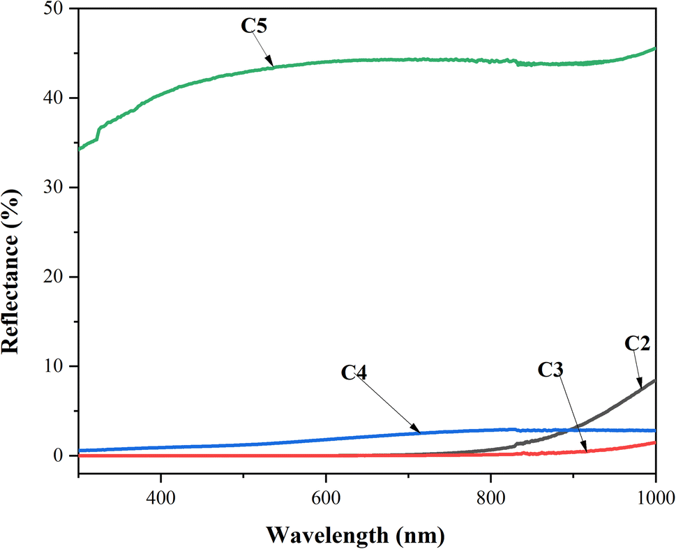
UV-visible spectroscopy was performed at room temperature to characterize the optical transmittance (T) and reflection (R) of the CZTS thin films with different copper concentrations in the spectral range of 280–1000 nm, as shown in Fig. 5. As the Cu concentration increased to 2 M, the samples exhibited lower transmittance and reflectance. Further, it is noteworthy that both R and T kept the movement constant as the wavelength increased, which was attributed to the good deposition of the CZTS thin films. The C3 and C4 samples presented the lowest transmittance and reflectance, which confirmed that these thin films absorbed the majority of the radiation, while C5 showed the maximum transmittance and reflectance.
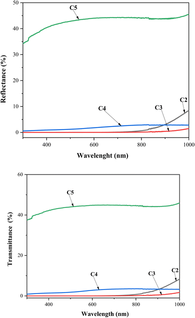 |
| | Fig. 5 Transmittance and reflectance spectra vs. wavelength for CZTS thin films prepared at different copper concentrations for samples: C2, C3, C4, and C5. | |
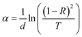
The absorption coefficient α was determined from the transmittance and reflectance results for the CZTS films obtained with different copper concentrations using the following relation:
| |
 | (4) |
where
d is the film thickness estimated from the SEM image (
Fig. 4e). All the thin films had absorption coefficients between (10
4 to 10
5 cm
−1), which shows an improvement in the quality of the prepared absorber materials, and makes them suitable for use as absorber layers in solar cell devices.
Absorbance is an important property of CZTS thin films, as they are considered absorber materials. Fig. 6 presents the spectra of the five samples, where it can be seen that their absorbance decreased with increasing the wavelength; however, C3 presented the highest value of absorbance (2.68%), Furthermore, thicker layers of CZTS tended to have a higher absorbance due to the longer path length of the light through the material, which was the case for sample C3, representing the film prepared with 1.5 M copper concentration. As the thickness is related to the rpm, so this can also affect the absorbance of the kesterite. Islam et al. found that the absorbance decreased with the rpm, and the optimum rpm was found to be 2500 rpm for spin-coating kesterite.34
 |
| | Fig. 6 Absorbance spectra vs. wavelength for the CZTS thin films prepared at different copper concentrations for samples: C2, C3, C4, and C5. | |
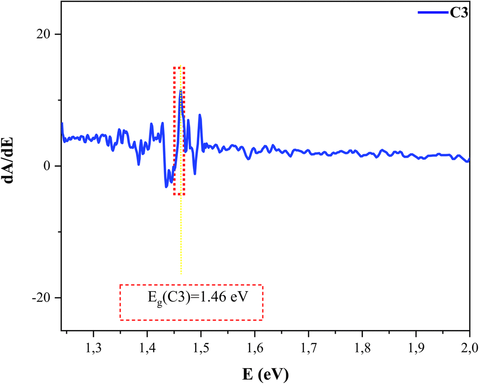
The band gap energy was calculated using the first derivative of the absorbance with respect to the energy (dA/dE), with the maximum peak of the derived spectrum and the lower side of the energy giving the band gap energy, as shown in Fig. 7. The band gap values of the CZTS thin films with different Cu concentrations are presented in Table 4. We noted that the band gap energy decreased with the increase in the crystalline size D calculated from XRD until 1.5 M copper concentration. Further, it has been clearly reported that the larger the grain size, the smaller the band gap. This behavior can be explained by the confinement effect.36 Khare et al. showed there was an increase in the optical band gap with a decrease in the crystalline size.37,39 All the samples were found to be near optimum for CZTS photovoltaic solar conversion in a single-band-gap device, and they exhibited better optical properties for solar cell applications.38–40 Note that the optical band gaps found in all the samples were in the optimum range for photovoltaic applications.
 |
| | Fig. 7 Variation of dA/dE versus E for the CZTS thin films prepared at the copper concentration of 1.5 M for sample C3. | |
Table 4 Band gap energies of the samples C1, C2, C3, C4, C5 of CZTS thin films
| Samples |
Gap energy (eV) |
| C1 (0.5 M) |
1.58 |
| C2 (1 M) |
1.5 |
| C3 (1.5 M) |
1.46 |
| C4 (2 M) |
1.53 |
| C5 (2.5 M) |
1.49 |
3.5. Electrical properties
The electrical characteristics of CZTS thin films with different copper concentrations were determined using the four-point method. Table 5 lists the conductivities and resistivities of the CZTS thin films. It is noticeable that all the films were p-type, and on the verge of being suitable for heterojunction solar cells with n-type layers. Besides, the copper concentration has an effect on the electrical performance of the films, and here C3 showed the maximum of conductivity (18.5 Ω−1 cm−1) corresponding to a minimum of resistivity (5.38 × 10⁻² Ω cm). The resistivity values were compared with those obtained by Tanaka et al. for CZTS thin films obtained by a dip-coating method41 and by Daranfed et al. for CZTS thin films synthesized by spray pyrolysis.42 The obtained electrical resistivity values are suitable for solar cell applications.43 Furthermore, the electrical properties of sample C5 have not been uploaded owing to the Cu-rich conditions; these latter conditions make the film disadvantageously critical, and full of dislocations, whereby the four points were unreachable.
Table 5 Hall effect characteristics: Conductivity and resistivity of the C1, C2, C3, C4 CZTS thin films
| Samples |
Conductivity (Ω−1 cm−1) |
Resistivity (Ω cm) |
| C1 |
5.4 × 10⁻⁴ |
1.83 × 10³ |
| C2 |
3.14 × 10⁻⁴ |
1.62 × 10³ |
| C3 |
1.85 × 101 |
5.38 × 10⁻² |
| C4 |
4.73 |
2.11 × 10⁻¹ |
| C5 |
— |
— |
4. Simulation SCAPS-1D
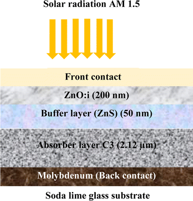
Simulation is an essential tool for fully understanding the performance of CZTS thin film solar cells. In this study, a solar cell capacitance simulator (SCAPS 1D) program was used. This software provides some descriptive factors of solar cells, such as the open-circuit voltage Voc, short-circuit current density Jsc, FF fill factor, and η efficiency. The findings in this study give great hope for CZTS thin films as better candidates for the absorber layer in a solar cell, especially sample C3 synthesized with 1.5 M copper molarity. This sample showed great crystallinity, optimum values for optical properties, and good electrical conductivity. A solar cell was fabricated with the structure shown in Fig. 8. This was composed of a p-type CZTS absorber layer, n-buffer layer (ZnS), and n-type i:ZnO. Molybdenum (Mo) was inserted as a back-contact metal on a glass substrate. Mahbub et al. found that a solar cell with a ZnS buffer layer had the highest efficiency (efficiency = 26.82%, FF = 69.44%, Jsc = 53.312 mA cm−2, and Voc = 0.724 V) among a range of considered buffer layers, such as CdS, In2S3, and ZnSe.44 The physical parameters of CZTS, ZnS, and ZnO:I used in the simulation46 are listed in Table 6. For sample C3, the important input parameters used in the simulation were adopted from the results obtained above. Note that all the parameters were considered to be constant during the simulation. The default illumination spectrum and operating temperature were set to the global AM1.5 standard and 300 K, respectively.
 |
| | Fig. 8 Solar cell structure using the C3 sample as the absorber layer. | |
Table 6 Physical parameters used in the simulation
| Material properties |
CZTS |
CdS34,36,37 |
ZnS34,36,37 |
i-ZnO34,36,37 |
| Experimental data. |
| Thickness [μm] |
2.12a |
0.050 |
0.050 |
0.200 |
| Bandgap (Eg) [eV] |
1.46a |
2.400 |
2.700 |
3.350 |
| Electron affinity χ, [eV] |
4.5 |
4.000 |
4.300 |
4.350 |
| Dielectric permittivity ε, [cm3] |
13.600 |
10.000 |
10.000 |
9.000 |
| CB density of states [cm−3] |
2.200 × 10¹⁸ |
2.200 × 10¹⁸ |
2.200 × 10¹⁸ |
2.200 × 10¹⁸ |
| VB density of states [cm−3] |
1.800 × 10¹⁹ |
1.800 × 10¹⁸ |
1.800 × 10¹⁸ |
1.800 × 10¹⁸ |
| Electron mobility [cm2 V s−1] |
1.000 × 10²a |
2.500 × 101 |
1.000 × 10² |
2.500 × 101 |
| Hole mobility [cm2 V s−1] |
4.433 × 101a |
1.000 × 10² |
2.500 × 101 |
1.000 × 10² |
| Donor density [cm−3] |
1.000 × 10¹⁷a |
1.000 × 10¹⁸ |
1.000 × 10¹⁷ |
1.000 × 10¹⁸ |
| Acceptor density [cm−3] |
1.000 × 10¹⁸a |
0.000 × 100 |
0.000 × 100 |
0.000 × 100 |
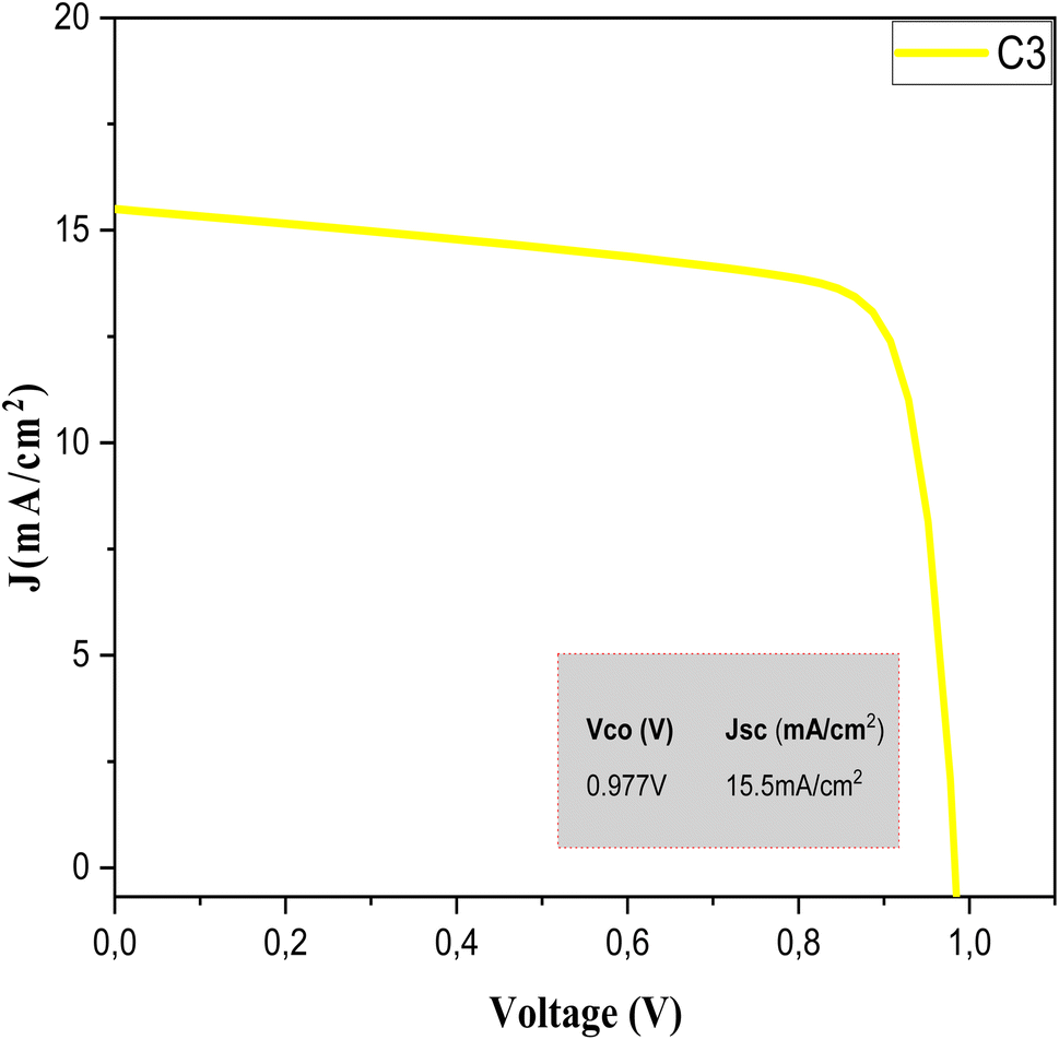
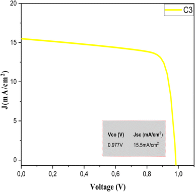
The SCAPS 1D results are shown in Fig. 9. The variation of the simulation current versus the voltage of the sample C3 absorbent layer can be clearly seen. The important descriptive parameters of SCAPS 1D, namely the Voc, Jsc, FF, and efficiency η, are listed in Table 7.
 |
| | Fig. 9 J–V characteristics of the CZTS thin films prepared with a copper concentration of 1.5 M for sample C3. | |
Table 7 Simulation SCAPS-1D results: Efficiency η, Vco open-circuit voltage, Jsc short-circuit current density, and FF fill factor of a CZTS solar cell made with sample C3
| Sample |
H (%) |
FF (%) |
Vco (V) |
Jsc (mA cm−2) |
| C3 |
11.6 |
76.31 |
0.977 |
15.5 |
A solar cell using ZnS as a buffer layer was reported with excellent results, such as a high efficiency of 11.6%. In addition, ZnS is considered to be an earth-abundant and non-toxic material, which is beneficial for the final solar cell. Some researchers have used CdS as a buffer layer in the final structure of a CZTS solar cell, while this latter is not considered clean and ecofriendly as CdS is a toxic layer, This variation in the buffer layers could be due to the critical importance of the density of the interfacial states, which increases with the increase in the CdS layer thickness and results in a decrease in the solar cell performance.45,47
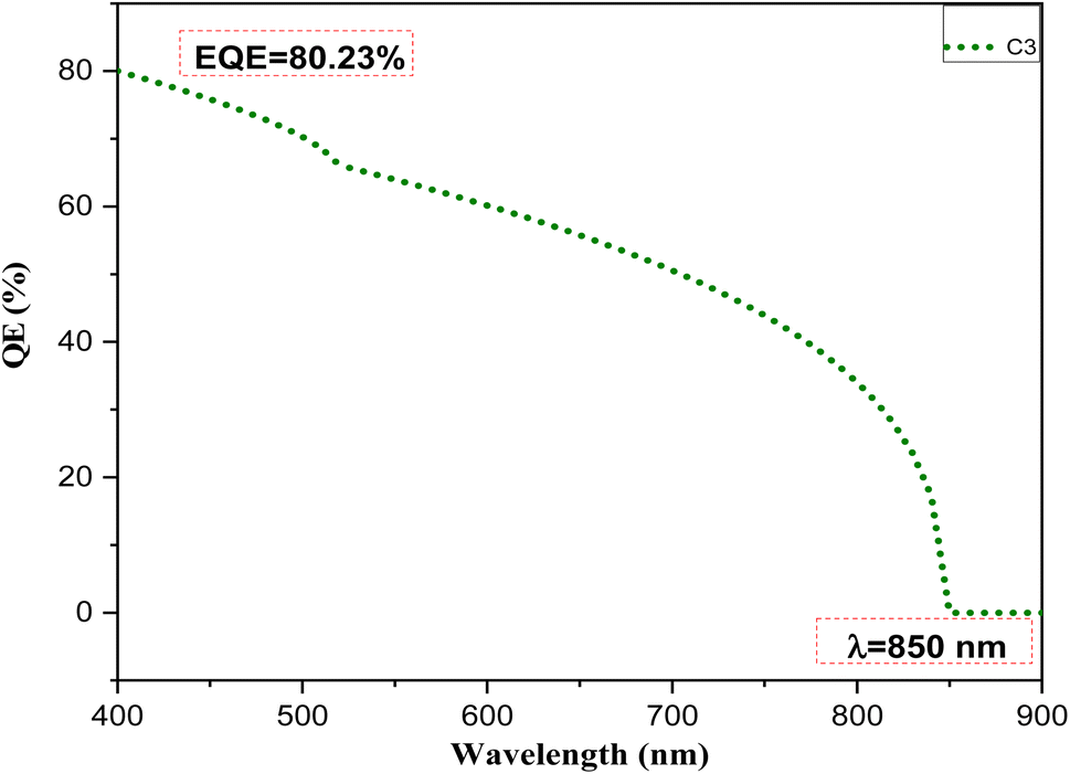
To gain further insights into the device performance, the external quantum efficiency (EQE) versus wavelength was plotted, as shown in Fig. 10. The EQE is the ratio of the number of charge carriers collected by the solar cell to the number of incident photons received by that cell. The sample C3 showed a significantly high percentage of EQE (80.23%) in the wavelength region from 400–900 nm. The curve shows absorption behavior at a wavelength of 850 nm. This result matched well with the band gap of the sample calculated from the optical properties.
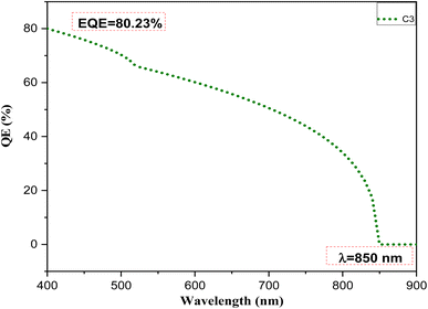 |
| | Fig. 10 EQE versus the wavelength for sample C3. | |
Fig. 11 presents the Band diagram of the Mo/CZTS/ZnS/ZnO:S cell using C3 as an absorber layer. The band alignment and the spike-like conduction make the transition of the electrons from the p-CZTS absorber layer to the buffer layer happen smoothly, thereby improving the open-circuit voltage (Voc) and the fill factor, and thus the performance of the solar cell.
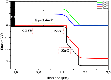 |
| | Fig. 11 Band diagram of the Mo/CZTS/ZnS/ZnO:S cell. | |
These results are in good agreement with those in the literature.48,49 Sample C3 provided an optimized, promising, and good efficiency. Therefore, this sample has good potential for use as an absorbent layer.
5. Conclusions
CZTS thin films were deposited on simple soda lime glass substrates by spin-coating using the sol–gel method without using any hazardous materials or environment (such as sulfurization or selenization). The effects of the copper molarity on the structural, morphological, elemental composition, optical, and electrical properties of the CZTS thin films were investigated. The XRD results revealed a polycrystalline structure, and the highest peak was along the (112) plane, corresponding to the kesterite phase of the CZTS thin films. Raman spectra were used to confirm the phase purity and prove the existence of the CZTS kesterite structure. The SEM image of sample C3 indicated a homogenous and uniform surface morphology with a thickness size of 2.12 μm. The optical band gap energy values were found to be optimum for use as absorber layers. The observed characteristics and results obtained in this study support the use of spin-coated CZTS films as absorber layers in thin film solar cells. SCAPS-1D was used for the numerical simulation of the CZTS solar cell by exploiting the data from the experimental work. The highest efficiency of 11.6% was achieved using SCAPS with ZnS as a buffer layer.
Conflicts of interest
The authors declare that they have no conflict of interest.
Acknowledgements
The authors declare that no funds, grants, or other support were received during the preparation of this manuscript.
Notes and references
- F. Z. Ramadan, F. Djeffal, L. B. Drissi, S. Saidi and H. Ferhati, J. Phys. Chem. Solids, 2021, 110458 Search PubMed.
- P. Fan, Z. Xie, G. Liang, M. Ishaq, S. Chen, Z. Zheng, C. Yan, J. Huang, X. Hao, Y. Zhang and Z. Su, J. Energy Chem., 2021, 61, 186–194 CrossRef CAS.
- D. Shin, B. Saparov and D. B. Mitzi, Adv. Energy Mater., 2017, 7, 1602366 CrossRef.
- A. Wang, N. L. Chang, K. Sun, C. Xue, R. J. Egan, J. Li, C. Yan, J. Huang, H. Rong, C. Ramsden and X. Hao, Sustainable Energy Fuels, 2021, 5, 1044–1058 RSC.
- A. Louwen, W. Van Sark, R. Schropp and A. Faaij, Sol. Energy Mater. Sol. Cells, 2016, 147, 295–314 CrossRef CAS.
- K. Zweibel, Science, 2010, 328, 699–701 CrossRef CAS PubMed.
- A. Walsh, S. Chen, S.-H. Wei and X.-G. Gong, Adv. Energy Mater., 2012, 2, 400–409 CrossRef CAS.
- E. M. Mkawi, K. Ibrahim, M. K. M. Ali and A. S. Mohamed, Int. J. Electrochem. Sci., 2013, 8, 359–368 CrossRef CAS.
- T. Shibuya, Y. Goto, Y. Kamihara, M. Matoba, K. Yasuoka, L. A. Burton and A. Walsh, Appl. Phys. Lett., 2014, 104, 021912 CrossRef.
- K. Ç. Demir, Mater. Sci. Semicond. Process., 2021, 123, 105553 CrossRef CAS.
- A. Ziti, B. Hartiti, H. Labrim, S. Fadili, A. Batan, A. Ridah and P. Thevenin, IOP Conf. Ser.: Mater. Sci. Eng., 2020, 948, 012025 CAS.
- M. I. Fathima, A. M. S. Arulanantham and K. S. J. Wilson, Mater. Res. Express, 2019, 7(1) DOI:10.1088/2053-1591/ab63f9.
- J. Jiang, L. Zhang, W. Wang and R. Hong, Ceram. Int., 2018, 44, 11597–11602 CrossRef CAS.
- N. Akcay, E. P. Zaretskaya and S. Ozcelik, J. Alloys Compd., 2019, 772, 782–792 CrossRef CAS.
- J.-F. Guillemoles, T. Kirchartz, D. Cahen and U. Rau, Nat. Photonics, 2019, 13, 501–505 CrossRef CAS.
- H. Katagiri, K. Jimbo, S. Yamada, T. Kamimura, W. S. Maw, T. Fukano, T. Ito and T. Motohiro, Appl. Phys. Express, 2008, 1, 0412011–0412012 Search PubMed.
- T. K. Todorov, J. Tang, S. Bag, O. Gunawan, T. Gokmen, Y. Zhu and D. B. Mitzi, Adv. Energy Mater., 2013, 3, 34–38 CrossRef CAS.
- W. Wang, M. T. Winkler, O. Gunawan, T. Gokmen, T. K. Todorov, Y. Zhu and D. B. Mitzi, Adv. Energy Mater., 2014, 4, 1–5 Search PubMed.
- A. Haddout, A. Raidou and M. Fahoume, Appl. Phys. A: Mater. Sci. Process., 2019, 125, 124 CrossRef.
- S. E. Lachhab, A. Bliya, E. Al Ibrahmi and L. Dlimi, Optik, 2022, 252, 168514 CrossRef CAS.
- F. Ynineb, M. Khammar, S. Guitouni, A. Hafdallah, N. Attaf and M. S. Aida, Appl. Phys. A: Mater. Sci. Process., 2021, 127, 1–7 CrossRef.
- N. J. Choudhari, Y. Raviprakash, F. Bellarmine, M. S. Ramachandra Rao and R. Pinto, Sol. Energy, 2020, 201, 348–361 CrossRef CAS.
- M. Burgelman, J. Verschraegen, S. Degrave and P. Nollet, Prog. Photovolt., 2004, 12, 143–153 CrossRef CAS.
- F. Aslan, A. Göktaş and A. Tumbul, Mater. Sci. Semicond. Process., 2016, 43, 139–143 CrossRef CAS.
- S. M. Bhosale, M. P. Suryawanshi, J. H. Kim and A. V. Moholkar, Ceram. Int., 2015, 41, 8299–8304 CrossRef CAS.
- M. Suryawanshi, S. W. Shin, W. R. Bae, K. Gurav, M. G. Kang, G. Agawane, P. Patil, J. H. Yun, J. Y. Lee, A. Moholkar and J. H. Kim, Phys. Status Solidi A, 2014, 211, 1531–1534 CrossRef CAS.
- A. Tumbul, F. Aslan, A. Goktas, M. Z. Zarbali and A. Kilic, Mater. Chem. Phys., 2021, 258, 123997 CrossRef CAS.
- J. Ghosh, S. Mazumdar, M. Das, S. Ghatak and A. K. Basu, Mater. Res. Bull., 2008, 43, 1023–1031 CrossRef CAS.
- A. Ziti, B. Hartiti, H. Labrim, S. Fadili, H. J. Tchognia Nkuissi, A. Ridah, M. Tahri and P. Thevenin, Appl. Phys. A: Mater. Sci. Process., 2019, 125, 218 CrossRef CAS.
- T. Shiyani, M. Patel, I. Mukhopadhyay and A. Ray, IETE Tech. Rev., 2016, 33, 2–6 CrossRef.
- S. A. Vanalakar, S. W. Shin, G. L. Agawane, M. P. Suryawanshi, K. V. Gurav, P. S. Patil and J. H. Kim, Ceram. Int., 2014, 40, 15097–15103 CrossRef CAS.
- M. J. Šćepanović, M. Grujić-Brojčin, Z. D. Dohčević-Mitrović and Z. V. Popović, Sci. Sintering, 2009, 41, 67–73 CrossRef.
- N. M. Shaalan, A. Z. Mahmoud and D. Hamad, Mater. Sci. Semicond. Process., 2020, 120, 105318 CrossRef CAS.
- S. Islam, M. A. Hossain, H. Kabir, M. Rahaman, M. S. Bashar, M. A. Gafur, A. Kabir, M. M. R Bhuiyan, F. Ahmed and N. Khatun, Int. J. Thin Film Sci. Technol., 2015, 4, 155 Search PubMed.
- S. Jain, S. Kumar Swami, V. Dutta and S. Narain Sharma, Inorg. Chem. Commun., 2021, 133, 108879 CrossRef CAS.
- A. Walsh, S. Chen, X. G. Gong and S. H. Wei, AIP Conf. Proc., 2011, 1399, 63–64 CrossRef CAS.
- A. Khare, A. W. Wills, L. M. Ammerman, J. Norris and E. S. Aydil, Chem. Commun., 2011, 11721–11723 RSC.
- D. A. R. Barkhouse, O. Gunawan, T. Gokmen, T. K. Todorov and D. B. Mitzi, Prog. Photovolt., 2015, 20, 6–11 CrossRef.
- G. Rey, G. Larramona, S. Bourdais, C. Choné, B. Delatouche, A. Jacob, G. Dennler and S. Siebentritt, Sol. Energy Mater. Sol. Cells, 2018, 179, 142–151 CrossRef CAS.
- R. J. Deokate, R. S. Kate and S. C. Bulakhe, J. Mater. Sci.: Mater. Electron., 2019, 30, 3530–3538 CrossRef CAS.
- T. Tanaka, T. Sueishi, K. Saito, Q. Guo, M. Nishio, K. M. Yu and W. Walukiewicz, J. Appl. Phys., 2012, 111, 3–7 Search PubMed.
- W. Daranfed, M. S. Aida, N. Attaf, J. Bougdira and H. Rinnert, J. Alloys Compd., 2012, 542, 22–27 CrossRef CAS.
- X. Yu, A. Ren, F. Wang, C. Wang, J. Zhang, W. Wang, L. Wu, W. Li, G. Zeng and L. Feng, Int. J. Photoenergy, 2014, 2014, 1–7 Search PubMed.
- R. Mahbub, M. Saidul Islam, F. Anwar, S. Sarwar Satter and S. Mahmud Ullah, South Asian J. Eng. Technol., 2016, 2, 1–10 Search PubMed.
- M. Kumar, A. Dubey, N. Adhikari, S. Venkatesan and Q. Qiao, Energy Environ. Sci., 2015, 8, 3134–3159 RSC.
- A. Houimi, S. Y. Gezgin, B. Mercimek and H. Ş. Kılıç, Opt. Mater., 2021, 121, 111544 CrossRef CAS.
- V. Hernández-Calderón, O. Vigil-Galán, M. Guc, A. Carrillo-Osuna, S. Ramírez-Velasco, F. J. Sánchez-Rodríguez, P. Vidal-Fuentes, S. Giraldo, E. Saucedo and Y. Sánchez, ACS Appl. Energy Mater., 2020, 3, 6815–6823 CrossRef.
- O. K. Simya, A. Mahaboobbatcha and K. Balachander, Superlattices Microstruct., 2015, 82, 248–261 CrossRef CAS.
- A. R. Latrous, R. Mahamdi, B. N. Touafek and M. Pasquinelli, Int. J. Thin Film Sci. Technol., 2021, 10, 59–65 CrossRef PubMed.
|
| This journal is © The Royal Society of Chemistry 2023 |
Click here to see how this site uses Cookies. View our privacy policy here. 
 Open Access Article
 This Open Access Article is licensed under a Creative Commons Attribution-Non Commercial 3.0 Unported Licence
 ,
Elyazid El mahboub
,
Elyazid El mahboub