
 Open Access Article
 This Open Access Article is licensed under a Creative Commons Attribution-Non Commercial 3.0 Unported Licence
Effect of long chain fatty acids on the memory switching behavior of tetraindolyl derivatives†
Surajit Sarkara,
Hritinava Banika,
Farhana Yasmin Rahmana,
Swapan Majumdarb,
Debajyoti Bhattacharjeea and
Syed Arshad Hussain *a
*a
aThin Film and Nanoscience Laboratory, Department of Physics, Tripura University, Suryamaninagar, 799022, West Tripura, Tripura, India. E-mail: sa_h153@hotmail.com; sahussain@tripurauniv.ac.in
bDepartment of Chemistry, Tripura University, Suryamaninagar, 799022, West Tripura, Tripura, India
First published on 4th September 2023
Abstract
Non-volatile memory devices using organic materials have attracted much attention due to their excellent scalability, fast switching speed, low power consumption, low cost etc. Here, we report both volatile as well as non-volatile resistive switching behavior of p-di[3,3′-bis(2-methylindolyl)methane]benzene (Indole2) and its mixture with stearic acid (SA). Previously, we have reported the bipolar resistive switching (BRS) behavior using 1,4-bis(di(1H-indol-3-yl)methyl)benzene (Indole1) molecules under ambient conditions [Langmuir 37 (2021) 4449–4459] and complementary resistive switching (CRS) behavior when the device was exposed to 353 K or higher temperature [Langmuir 38 (2022) 9229–9238]. However, the present study revealed that when the H of –NH group of Indole1 is replaced by –CH3, the resultant Indole2 molecule-based device showed volatile threshold switching behaviour. On the other hand, when Indole2 is mixed with SA at a particular mole fraction, dynamic evolution of an Au/Indole2-SA/ITO device from volatile to non-volatile switching occurred with very good device stability (>285 days), memory window (6.69 × 10²), endurance (210 times), data retention (6.8 × 10⁴ s) and device yield of the order of 78.5%. Trap controlled SCLC as well as electric field driven conduction was the key behind the observed switching behaviour of the devices. In the active layer, trap centers due to the SA network may be responsible for non-volatile characteristics of the device. Observed non-volatile switching may be a potential candidate for write once read many (WORM) memory applications in future.
Introduction
Resistive switching (RS) based memory devices can be considered as one of the possible contenders to fulfill the requirement of new generation memory devices, because of its excellent scalability, fast switching speed, low power consumption etc.1–6 The existing Si based devices have reached fundamental limitations like downscaling, power consumption, heat dissipation, expensiveness etc. and it is very difficult to enhance their performance as well.7 In this regard, organic materials have shown great potential in the last two decades to address the scientific challenges appearing for Si based devices and enable the manufacture of different types of thin film based electronic devices with improved performances.8–11 Important features like low cost, easy fabrication, down scalability, and mechanical flexibility make organic materials attractive towards designing electronic devices.12 In addition to this RS memory employing organic materials is very emerging due to their high data retention, low power consumption as well as ability to achieve a high density crossbar array structure.8–11Resistive switching (RS) refers to the physical phenomena where a dielectric/insulator sandwiched between two electrodes suddenly changes its resistance under the action of electric field. Such devices possess two stable states – (i) low conducting OFF state or high resistance state (HRS) and (ii) high conducting ON state or low resistance state (LRS).8,13,14 This allows the application of RS devices towards memory concepts.8 Two resistance states HRS and LRS considered as binary “0” and “1”.15 The device can be switched between the HRS and LRS at a particular bias voltage. In some cases when the device switched from HRS to LRS state upon application of bias, the device retained the LRS state even when reverse bias is applied or the bias is withdrawn.15 The device never returned back to its HRS state. This means here the device shows the irreversibility as well as non-volatility.15 Devices with such behavior are suitable for write once read many (WORM) like memory applications.15 Based on volatility as well as data retention behaviour there are other types of memory applications employing RS devices.15,16
It has been observed that materials having easily polarisable structures are appropriate for the fabrication of organic electronic devices.17,18 In this regard, organic molecules containing a conjugated π-system end-capped with a strong electron-donor group and/or a strong electron-acceptor group shows a push–pull system (D–π–A) which ensures intermolecular charge transfer as well as low energy barriers. Later, various five- and six-membered heterocycles can be utilized as suitable π-conjugated backbones as they act as auxiliary donors or acceptors. This improves the overall polarizability of the chromophore and the performance of organic electronic devices.19–21 In this context, heterocyclic systems such as indole derivatives are gaining much attention due to their π-conjugation and the presence of the –NH group on their pyrrole ring. Recently, we have synthesized 1,4-bis(di(1H-indol-3-yl)methyl)benzene (Indole1) and demonstrated bipolar resistive switching employing Indole1 suitable for resistive random access memory (RRAM) applications.8 Interestingly it has been observed that when the Indole1 based RS device is exposed to 353 K or higher temperature dynamic evaluation of the device from bipolar resistive switching (BRS) to complementary resistive switching (CRS) occurred.9 Such CRS devices are more advantageous compared to BRS devices for many applications in terms of minimizing the sneak path problem appeared in BRS having crossbar array structure.22 It has been reported that oxidation reduction due to the presence of –NH group on the pyrrole ring of Indole1 molecule played vital role towards the observed RS behaviors.8
It is well known that upon modification of functional group in the organic molecule it's possible to have different functionality as well as improved device performances.23,24 Also it has been reported that incorporation of suitable matrix materials (nanoparticle, quantum dots, long chain fatty acid etc.) within the active layer may act as trap centre resulting WORM behaviours.25,26 However, mixing as well as interaction and organization of the matrix materials within the active layer is very crucial for the device performance and depending on that different types of switching with varying performance may be observed.11,26–30 Accordingly, in the present case, the structure of Indole1 molecule has been modified where the H of –NH group of Indole1 has been replaced by –CH3. This has been done to oppose the oxidation-reduction phenomenon responsible for observed bipolar resistive switching (BRS) in the previous report.8 It has been observed that I–V behavior of the devices with modified tetraindolyl derivative p-di[3,3′-bis(2-methylindolyl)methane]benzene (Indole2) as well as their mixture with stearic acid (SA) showed interesting results. Here, Indole2 based device showed threshold switching behavior. On the other hand, in case of Indole2–SA mixed devices with 0.3 M of Indole2 showed non-volatile resistive switching suitable for write once read many (WORM) type memory applications with very high device stability, device yield with optimum performance. The permanent data storage nature of WORM memory makes them useful for several applications, where data security, reliability and long-term storage is important, such as archival storage devices, permanent storage, secure databases, electronic labels and so forth.12,16,31–33 Therefore, as a whole the series of investigations employing tetraindolyl derivatives revealed the realization of a variety of memory applications like RRAM,8 CRS,9 threshold and WORM (present report) memory by changing the microenvironment of the device as well as the molecular structure. Similar approaches can be taken to realize different kinds of RS devices by playing with the microenvironment as well as structure of molecules.
Experimental section
Materials
Synthesized organic material namely p-di[3,3′-bis(2-methylindolyl)methane]benzene (Indole2) has been used, which had been reported in our previous work.34 We have purchased stearic acid (C18H36O2) (SA) from Sigma-Aldrich Pvt. Ltd and used as received. Chemical structures of the molecules used are shown in Fig. 1. Spectrochem Pvt. Ltd provided us terephthaldehyde and DDQ and we used as received. Chloroform (spectroscopic grade) (SRL, India) were used as solvent to prepare solution. Sigma-Aldrich Pvt. Ltd provided us ITO coated glass substrate with a resistivity of 70–100 Ω Sq−1. We have cleaned ITO surfaces through successive ultrasonication in three solvents (5 min for each) isopropyl alcohol, chloroform and deionized water one by one. After that, it was dried using N2 gas blow at room temperature.35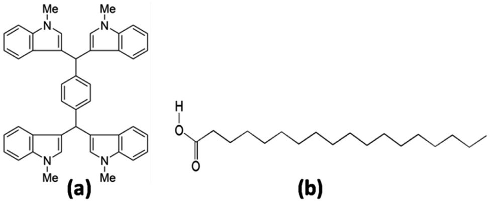 | ||
| Fig. 1 Chemical structure of (a) p-di[3,3′-bis(2-methylindolyl)methane]benzene (Indole2) and (b) Stearic acid (SA). | ||
Resistive switching device fabrication
Indole2 molecules were used to fabricate resistive switching devices with the configuration Au/Indole2/ITO. For all devices, ITO was employed as the bottom electrode and gold (Au) as the top electrode. In order to fabricate the device, we used a spin-coating film deposition equipment (Model: EZ spin-SD, Apex Instruments Co., India) to deposit Indole2 molecules and Indole2-SA mixed system in different mole fractions onto an ITO coated glass slide. In order to deposit flatness of the contact surface is important since the morphology of active layer affects the conduction behavior.26 It has been observed that the deposition technique also play important role in the RS device performances.8 Almost reproducible switching behavior is observed for different memory cell where the active layer is deposited through spin coating technique. Chloroform solution of Indole2 (1 mM) and mixture of Indole2 and SA (1 mM) with Indole2 mole fraction 0.8, 0.5 and 0.3 was spread drop-wise over a cleaned ITO slide and then spun to spread the sample solution almost uniformly throughout the whole surface of the slide. The substrate was spun at 1500 rpm for 120 seconds for every 1 drop of sample solution on the slide. The spin-coating technique has been described in detail elsewhere.36 After depositing the active layer onto the ITO, the film has been vacuum dried for at least 10 hours in vacuum desiccator before gold electrode deposition. Array of circular gold electrodes were deposited using a mask through sputtering technique. The average diameter of the gold pads was of the order of 500 μm. Fig. S1 of ESI† depicts a schematic illustration of the device structure.Measurements of I–V characteristics
The I–V characteristics of the device with the configuration Au/Indole2/ITO and Au/Indole2-SA/ITO were investigated using a Keithley SourceMeter (Sl No. 2401). The fabricated devices were vacuum dried for at least 10 hours before being measured. Since, the device is prepared in open atmosphere at room temperature; moisture may be present in the active layer of the device. As a result I–V behavior of the device may be compromised. Also with aging due to drying of the active layer the device characteristics may alter. Vacuum drying helps to avoid such problem resulting reliable switching behavior with very good stability. During the experiment, I–V characteristics were determined in several sweep directions with a step potential of 0.03 V for device 1–device 3 and 0.02 V for device 4.FESEM imaging
Surface morphology of the active layer of the device as well as the cross-sectional view of the RS device was measured using Field Emission Scanning Electron Microscope (FESEM), model no. Sigma 300, Zeiss Pvt. Ltd. The operating acceleration voltage was 5 kV.Isotherm measurement and film preparation using Langmuir–Blodgett (LB) technique
π–A isotherms were investigated using LB film deposition instrument (Apex 2000C, Apex Instruments Co., India). In order to investigate the π–A isotherm chloroform solution of Indole2 and Indole2–SA mixture at different mole fraction were spread onto the subphase of pure Milli-Q water (18.2 MΩ cm−1) using a microsyringe. After evaporation of volatile solvent (chloroform) the π–A isotherm was recorded at a 5 mm min−1 barrier compression rate. A Wilhelmy plate arrangement was used to measure the π–A isotherm. In order to prepare LB film based device we have deposited 60 layer LB film onto ITO glass slide at surface pressure 25 mN m−1 with a deposition rate of 5 mm min−1. During film deposition transfer ratio was found to be in the range of 0.8 to 0.98. Details of the LB technique have been reported elsewhere.37Result and discussion
Fig. 2a shows the I–V characteristics of the designed Au/Indole2/ITO device, where Au acts as a top electrode and ITO acts as a bottom electrode. Scanning voltage ranges as well as scanning directions are also shown in the figure. Initially the device is in low conducting or high resistance states (HRS). Depending on the bias voltage the device changes its resistance states HRS to low resistance state (LRS) abruptly at a particular voltage 1.394 V, called the threshold voltage (VTh). Again during the reverse sweep (3 V to 0 V), the device returns to the initial state (i.e., HRS) at a particular scanning voltage 1.03 V. This voltage is typically known as holding voltage (Vh).38 Such switching behavior where the device switches from HRS to LRS during the forward sweep and again switches from LRS to HRS during the reverse sweep at the same polarity is known as Threshold Switching (TS).39–43 TS devices may be useful to resolve the sneak path problem in memory applications having crossbar array structure as a selector device.40 Similar behavior was also observed in case of negative polarity, where threshold voltage (VTh) was −1.636 V and holding voltage (Vh) was −1.437 V. | ||
| Fig. 2 I–V characteristics of the (a) Au/Indole2/ITO device (device 1) (b) Au/Indole2-SA/ITO device with Indole2 mole fraction 0.8 (device 2) (c) Au/Indole2-SA/ITO device with Indole2 mole fraction 0.5 (device 3) and (d) Au/Indole2-SA/ITO device with Indole2 mole fraction 0.3 (device 4). For all the cases compliance current was 1 mA. Inset of (d) represents the linear I–V behavior of device 4 without compliance current in negative polarity. | ||
In order to tune the memory performance as well as to check the variation in the memory switching behavior, a long chain fatty acid viz., SA has been incorporated within the Indole2 layer within the device.26 Here, three devices have been prepared with Indole2 and SA mixed film as the active layer having Indole2 mole fraction 0.8, 0.5 and 0.3. I–V curves of all the devices are also shown in Fig. 2.
It has been observed that Au/Indole2-SA/ITO devices with Indole2 mole fractions 0.8 (Fig. 2b) and 0.5 (Fig. 2c) also showed the threshold switching behavior similar to that of pure Indole2 based device, although slight variations in the memory performances are observed as shown in Table 1. However, interestingly the observed switching behavior changes completely for the device with Indole2 mole fraction less than 0.5. Corresponding I–V curves are shown in Fig. 2d (0.3 mole fraction) and Fig. S2 in ESI† (0.2 and 0.4 mole fraction). It has been observed that performance of the WORM device especially interms of device yield was very poor (<20%) for 0.2 and 0.4 mole fraction. Accordingly, Indole2–SA based WORM device for Indole2 mole fraction 0.3 has been analysed and characterized further, whereas 0.3 mole fraction memory performance was better. Here, the device (device 4) switched from HRS to high conducting LRS state at 1.47 V during positive sweep. When the scanning voltage is reversed the device never returned back to its HRS state. The HRS (OFF state) also can't be restored by applying the bias in either direction. Interestingly, it has also been observed that once the device is switched ON (LRS) it retains its ON state even when the bias is removed. This means here the device shows the irreversibility as well as non-volatility.31 Devices with such behavior are suitable for WORM like memory applications.31,44,45 During experiment the switching speed was found to be 100 ns.
| Device configuration | Switching type | Positive polarity | Negative polarity | Compliance current (mA) | Device yield (%) | ON–OFF ratio | |||
|---|---|---|---|---|---|---|---|---|---|
| Threshold voltage (VTh) (in V) | Holding voltage (Vh) (in V) | Threshold voltage (VTh) (in V) | Holding voltage (Vh) (in V) | ||||||
| Positive polarity | Negative polarity | ||||||||
| a VR = read voltage. | |||||||||
| Au/Indole2/ITO (device 1) | TS | 1.394 | 1.030 | −1.636 | −1.437 | 1 | 31 | 6.5 × 10² at VR![[thin space (1/6-em)]](https://www.rsc.org/images/entities/char_2009.gif) a = 1.06 V a = 1.06 V |
5.65 × 101 at VRa = 1.48 V |
| Au/Indole2-SA/ITO (mole fraction 0.8) (device 2) | TS | 2.06 | 1.303 | −2.63 | −2.151 | 1 | 40 | 1.74 × 101 at VRa = 1.5 V |
4.09 × 10² at VRa = 2.5 V |
| Au/Indole2-SA/ITO (mole fraction 0.5) (device 3) | TS | 1.636 | 1.091 | −2 | −1.545 | 1 | 46 | 8.81 × 10² at VRa = 1.2 V |
4.13 × 10² at VRa = 1.72 V |
| Au/Indole2-SA/ITO (mole fraction 0.3) (device 4) | WORM | 1.47 | — | — | — | 1 | 78.5 | 6.69 × 10² at VRa = 0.1V |
— |
A compliance current of 1 mA was used in order to limit the current flowing through the device. We have also checked the I–V behavior with no compliance during negative sweep and no significant change in the I–V behavior is observed (inset of Fig. 2d). However, it has been observed that device performance in terms of read endurance and retention is better when we apply compliance at 1 mA compared to that in absence of compliance. This may be due to the fact that during consecutive scan higher current flow through the device may damage/burn the active layer.46 We have also checked the I–V behavior with compliance 0.5 mA and 1 μA and reliable WORM behavior was observed. Corresponding plots are shown in Fig. S3 of ESI.†
Forming process is one of the concerns in case of RS memory.47 Basically the forming voltage refers to the voltage required to initiate the formation of a conductive filament or path in a resistive switching device. It is typically much higher than the operating voltage required to switch the device from a high-resistance state to a low-resistance state.16 This is highly undesirable because of CMOS-incompatible high voltages and the time-consuming necessity of addressing every individual cell on a chip prior to operation. In addition, this may induce significant device-to-device variation in performance.48,49 This variation may be due to fluctuations in filament size, shape, and location etc.50
In case of RS memory devices idea about the forming process can be obtained by applying multiple SET–RESET operation in a particular cell. For first initial scan the device switches from initial HRS to LRS at higher SET voltage compared to the SET voltages from second scan onwards.16 In the present case to have idea about forming voltage we have applied consecutive scan cycles for each devices. In case of TS devices (device 1–3) no significant and consistent decrease in SET or RESET i.e., VTh or Vh voltages were observed with respect to first initial scan. This negates the occurrence of the forming process. On the other hand in case of WORM devices (device 4), once the device is switched to its LRS state it never returned back to its HRS state again and retains the state permanently.51 Therefore, it's difficult to have idea about forming process by applying consecutive scans to a single device showing WORM behaviour. However, in order to have idea about device-to-device variation in VTh and Vh voltages, we have prepared several identical devices for each type of device and measured their I–V curves. Calculated relative deviations are shown in Fig. 3.
 | ||
| Fig. 3 Device to device cumulative probability distribution of threshold (VTh) and holding (Vh) voltages for (a) device 1, (b) device 2, (c) device 3 and (d) device to device cumulative probability distribution of SET (VTh) voltages for device 4. Inset represents the physical picture of the same device. | ||
In order to get an idea about the device reproducibility, device yield is an essential parameter in resistive memory devices.8,9,31 In order to do that we have prepared 42 (7 × 6 array structure) independent switching devices (cells) for all the four device configuration. Therefore, we have 42 identical devices for each of the four configurations. Physical picture of one of the device array has been shown in the inset of Fig. 3d. After preparing the devices we have measured the I–V behavior of the 42 identical devices for each configuration. In case of pure Indole2 based device (device 1) out of 42 devices 13 devices showed reproducible threshold switching indicating a device yield of the order of 31%. In case of Indole2–SA mixed system with Indole2 mole fraction 0.8 (device 2) and 0.5 (device 3) showed threshold switching with device yield 40% and 47.6% respectively. Device to device cumulative probability of VTh and Vh plots for those three device configurations are shown in Fig. 3a–c. For the device having Indole2–SA mixed system with Indole2 mole fraction 0.3 (device 4), out of 42 switchable devices 33 devices showed reproducible WORM characteristics. Corresponding cumulative distribution of the threshold voltages are shown in Fig. 3d. Relative deviation of SET (VTh) voltage was 4.63% with device yield of the order of 78.5%.
Although electronic applications employing organic materials are very promising but the main challenges are their inferior thermal as well as long term device stability.52,53 In the present case to check the device stability, I–V curves of all the designed devices have been measured with passage of time as well as exposing the devices at various temperatures. Different parameters of the corresponding I–V curves are listed in Table 2 and the results are shown in Fig. S4 of ESI.† It has been observed that all the devices (device 1–3) showed reproducible switching behavior up to 80 °C and it was 120 °C for device 4 indicating very good thermal stability. Devices exposed beyond that temperature lose their switching behavior. On the other hand it has been observed that TS devices (device 1 to device 3) showed almost reproducible switching behavior even beyond 60 days from the date of device prepared (Table 2).
| Device configuration | Thermal stability | Long term stability | ||||||||
|---|---|---|---|---|---|---|---|---|---|---|
| Up to (°C) | Relative deviation of | No. of days | Relative deviation of | |||||||
| Positive polarity | Negative polarity | Positive polarity | Negative polarity | |||||||
| VTh (%) | Vh (%) | VTh (%) | Vh (%) | VTh (%) | Vh (%) | VTh (%) | Vh (%) | |||
| Au/Indole2/ITO (device 1) | 80 | 5.56 | 4.31 | 6.2 | 7.5 | 66 | 4.05 | 5.12 | 5.24 | 11.08 |
| Au/Indole2-SA/ITO (mole fraction 0.8) (device 2) | 80 | 4.28 | 3.87 | 5.2 | 6.54 | 64 | 3.85 | 5.65 | 9.19 | 3.08 |
| Au/Indole2-SA/ITO (mole fraction 0.5) (device 3) | 80 | 3.54 | 2.18 | 8.52 | 3.56 | 68 | 10.48 | 6.32 | 3.82 | 4.56 |
| Au/Indole2-SA/ITO (mole fraction 0.3) (device 4) | 120 | 3.84 | — | — | — | 285 | 6.32 | — | — | — |
Idea about physical stability of the device is important from application point of view. In order to do that the I–V curve of a particular device has been measured with passage of time. During this period the device has been preserved under ambient condition and I–V characteristics of the device were recorded daily on a regular basis. Variations of humidity and temperature were 30 to 35% and 20 to 25 °C respectively during the study period. It has been observed that the designed WORM device (device 4) showed reproducible WORM characteristics even beyond 285 days with negligible variation in memory window (Table 2). Ideal mixing (Fig. 5a) between SA and Indole2 molecule at 0.3 M of Indole2 may play crucial role towards observed persistent WORM behavior with enhanced device stability for device 4.
In the previous section of the manuscript, it has been observed that device with Indole2–SA mixed film with Indole2 mole fraction 0.3 as the active layer (device 4) showed WORM memory behavior. However, for practical as well as commercial applications data sustainability as well as reproducibility of the proposed memory device is very crucial. Studies of endurance as well as data retention behavior of the device give idea about these issues.8,9,31 In case of WORM memory, once the data is written in the memory, it can be read again and again.31 Data retention characteristics indicate how long the device can retain the stored information once written, i.e., how long it can maintain a particular state once switched to it.54–56 It has been observed that in the present case the designed WORM device can retain its particular ON or OFF state up to 6.8 × 10⁴ s at a read voltage of 0.1 V with negligible deviation in the memory window. Plot of corresponding LRS and HRS resistances with time has been shown in Fig. 4a.
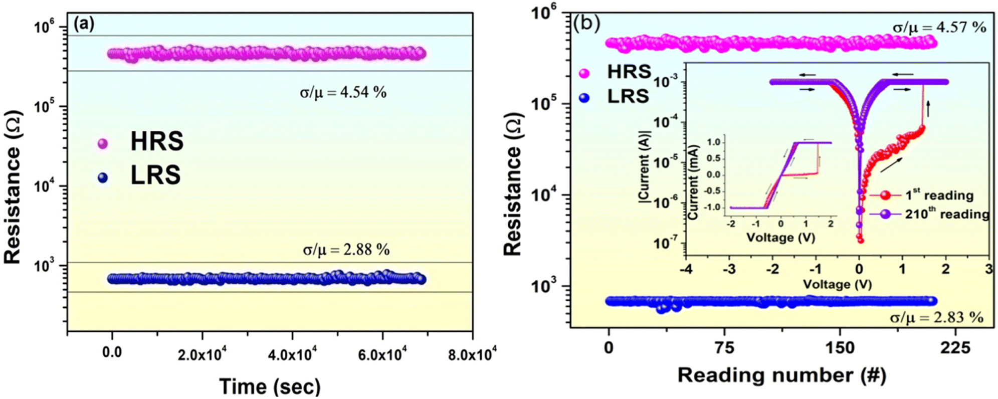 | ||
| Fig. 4 (a) Data retention characteristics of the device having configuration Au/Indole2-SA/ITO with Indole2 mole fraction 0.3 (device 4) over a time period of 6.8 × 10⁴ s and (b) endurance characteristics of the same device with 210 times. | ||
Data reproducibility i.e., read endurance for the designed device has also been investigated for both OFF and ON state. It was found that the WORM device SET from HRS to LRS at VTh = 1.47 V. Now in order to check the endurance for the OFF state, a voltage scan from 0 V to 1 V was applied such that the device remains at its high resistance OFF state following consecutive reading of the HRS resistance at read voltage 0.1 V. To check the ON state endurance the device has been switched to its ON state by applying voltage scan 0 V to 2 V followed by consecutive reading of ON state LRS values at 0.1 V. It has been found that the device can be read at least up to 210 times with negligible variation in memory window. Corresponding results are shown in Fig. 4b.
A comparison study in Indole2–SA based WORM memory with the similar reported result has been given in Table 3. From the Table 3 it has been observed that the present device may be suitable for future technological applications in terms of various memory parameters especially with physical stability more than 285 days. Physical stability of WORM memory employing organic molecule is very important. There is no report showing physical stability of WORM memory more than 285 days as per as literature survey.
| Device configuration | Threshold voltage (V) | Memory window | Retention (s) | Endurance | Stability (days) | Reference |
|---|---|---|---|---|---|---|
| Al/PBI/ITO | 3.8 | 104 | 104–106 | — | — | 57 |
| Al/imide/ITO | 1.9 | ∼104 | 4000 | — | — | 58 |
| Au/amido phenazine–SA/Au | −1.6 | >104 | 104 | — | 6 | 26 |
| Ag/D–π–A ester flanked quinolines/ITO | −1.21 to −2.12 | 103 | 103 | 100 | — | 59 |
| Al/PI/MLG/PI/Al | 3.5 | 106 | 104 | — | — | 60 |
| ITO/cobalt(II)bis–terpyridine complex/Au | ±3 | >103 | 103 | — | — | 61 |
| PEDOT:PSS/DNA/PEDOT:PSS | −2 | 104 | 104 | — | — | 62 |
| Ag/silk fibroin/Au | 1.3–3.4 | 107–108 | ∼104 | — | — | 63 |
| Au/PS/ITO | 1.33 | 4.57 × 10³ | ∼106 | 3.6 × 10⁴ | 210 | 31 |
| Ag/albumen/ITO | 2.2 | 2.0 × 10⁷ | 1.1 × 10⁵ | — | — | 64 |
| PFN/PBS-5 | 1.6 | 102 | 103 | — | — | 65 |
| Al/CSQDs-PVP/Pt | 1.6 | ∼105 | 3.2 × 10³ | 200 | — | 25 |
| Al/Au NPs: lignin/Al | 4.7 | >5 × 10³ | >103 | — | — | 66 |
| Au/Indole 3–SA/ITO (mole fraction 0.3) | 1.47 | 6.69 × 10² | 6.8 × 10⁴ | 210 | 285 | Present work |
In the previous section of the manuscript it has been observed that the WORM memory behavior was observed for the Indole2–SA mixed film based device (device 4) with Indole2 mole fraction of 0.3. All other devices under investigations showed threshold switching behavior. Therefore, it is assumed that mixing of Indole2 and SA might have played a role in this regard. In order to have idea about mixing behavior as well as nature of interactions among the binary components Langmuir monolayer analysis technique has been employed.37 Pressure–Area (π–A) isotherms of Indole2–SA mixed system at different mole fractions of Indole2 along with pure SA and Indole2 have been recorded. Corresponding curves are shown in Fig. S5 of ESI.† Upon compression both Indole2 and SA showed smooth rise of surface pressure. The lift-off area of SA was found to be 0.276 nm2 as determined by the method described by Chakraborty et al.67 The molecular areas of 0.23 nm2 and 0.21 nm2 at surface pressures of 15 and 25 mN m−1 of SA isotherm as well as the shape are in good agreement with the previously reported results.68 The lift-off area of Indole2 isotherm was 0.2 nm2. In case of mixed isotherms, most of the cases the lift off area lies in between lift off areas of pure Indole2 and SA. However, in few cases lift-off area become higher than the pure SA isotherm. This indicates the interactions between the SA and Indole2 molecules within the mixed systems.69
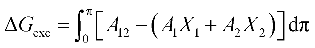
In order to shed further insights into the thermodynamic stability of the Indole2–SA mixed films compared to that of pure Indole2 and SA, Gibbs free energy (ΔGexc) analysis has been carried out using the following equations70,71
 | (1) |
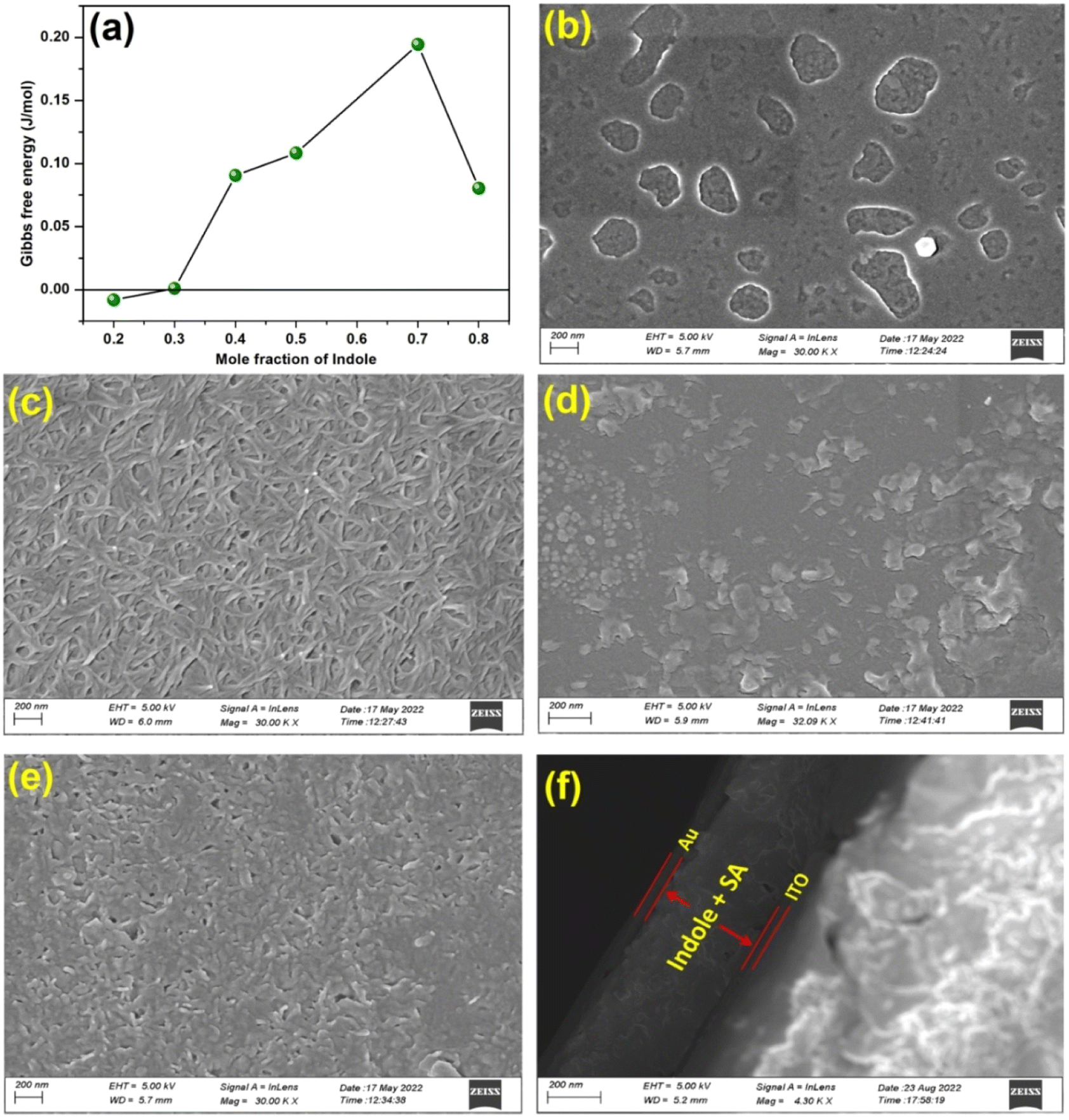 | ||
| Fig. 5 (a) Plot of Gibbs free energy versus mole fraction of Indole2. FESEM image of (b) pure Indole2, (c) pure SA, (d) Indole2–SA mixture with Indole2 mole fraction 0.5, (e) Indole2–SA mixture with Indole2 mole fraction 0.3 and (f) cross-sectional view of the device having configuration Au/Indole2-SA/ITO. All the films and devices were prepared using spin-coating technique. | ||
On the other hand, for higher mole fraction of Indole2 ΔGexc > 0 means the repulsion/positive interaction between Indole2 and SA molecules.70 Again at mole fraction lower than 0.3, ΔGexc < 0 indicating attractive interaction between them.70 Therefore, in both the cases, certain amount of de-mixing or immiscibility exists within the Indole2–SA mixed system except Indole2 mole fraction 0.3. Therefore, ideal mixing of Indole2 and SA in the mixed system of Indole2 mole fraction 0.3 may provide favourable condition for WORM switching to occur. In terms of chemical point of view, we know Indole nitrogen is not basic, so acid–base interaction between Indole2–stearic acid is ruled out. However, cation–π interaction is well known in many natural systems, particularly in the amino acid having an aromatic side chain.72,73 Therefore we assume that non-covalent bonding (aromatic –H+) may be responsible for molecular assembly in the present study.
We have also calculated compressibility modulus, Cs−1 from the pressure–area isotherm curves.74 Values of Cs−1 as well as peaks present in the Cs−1 versus π curve gives idea about physical state of the film associated with molecular packing and phase/ordering of molecules.74,75 Corresponding plot of Cs−1 versus π are shown in Fig. S6 of ESI.†
It has been observed that Cs−1 versus surface pressure (π) curves for Indole2 mole fraction up to 0.5 almost resembles the curves for pure SA in terms of peaks present. This indicates existence of similar phases in these films like that of SA films, where at higher surface pressure an ordered condensed film is formed.67 Although, here the extent of ordering depends on the Indole2 mole fraction as the Cs−1 value was different for different mole fractions.8,76 On the other hand curves for Indole2 mole fraction higher than 0.5 are different and only possess a broad flat nature indicating liquid phase.74,75,77 According to Davies and Rideal description liquid-expanded (LE) state of the film is associated with the modulus values within the range 12.5–50 mN m−1, whereas, the range 100–250 mN m−1 is related with liquid condensed (LC) state.74,75,77 Considering maximum value of Cs−1 it may be noted that mixed film up to 0.4 mole fraction possess LC phase, whereas, higher mole fractions the films possess only LE phase.74,75,77 I–V studies also revealed that device with Indole2 mole fraction 0.5 or higher showed threshold switching. On the other hand device with Indole2 mole fraction up to 0.4 mole fraction showed WORM behaviour. However, in case of 0.3 mole fraction maximum reliable device behaviour was observed. Therefore, LC phase as well as extent of ordering may play a crucial role towards the observed WORM behaviour.
In the present work device 4 showed non-volatile WORM behaviors (Fig. 2d) where the active layer (Indole2 + SA) of the device was deposited using spin coating technique. To have idea about the effect of deposition technique on switching, we have also designed device with similar structure like that of device 4 where the active layer was deposited using LB technique. Corresponding I–V curves are shown in Fig. S7 of ESI.† It has been observed here the device showed WORM behavior with compliance current 1 mA (Fig. S7a†). However, the device showed bipolar RRAM behavior with no compliance during reverse scan (Fig. S7b†). Although in case of spin coating based devices WORM behavior was observed even in absence of compliance during reverse scan. This observed difference in device behavior may be due the difference in molecular organization/packing in the active layer during deposition following two different techniques.
It may be mentioned that LB method is more powerful for controlling molecular orientation and hence a mixing state compared to spin coating.37 However, detail study is required to explore the exact reason behind this. Work is going on in our lab in this regard.
In order to have visual idea about the device structure as well as surface of the active layer of the devices, FESEM has been employed. Corresponding images are shown in Fig. 5b–f. For comparison, FESEM image of bare ITO has been given in Fig. S8 of ESI.† It has been observed that pure Indole2 and SA showed completely different surface topography. SA showed mesh/network like structures, whereas, Indole2 showed comparatively smoother appearance. In pure Indole2 FESEM image patchy areas are obtained. A close look and comparison with the FESEM image of bare ITO surface indicated that these areas are not empty rather there may exist some cluster or aggregates of Indole2 molecule. However in both the cases, surface coverage was very good. On the other hand, in case of mixed film with Indole2 mole fraction >0.3 showed the surface topography closer to pure Indole2 whereas, at mole fraction 0.3 showed surface topography closer to pure SA. Here, the visible SA network present within the Indole2–SA mixed film may act as the trap centers for the charge carriers while passing across the active layer of the material.26 H-Bonded complex between Indole2 and SA may creates electron deficiency on Indole2 skeleton that may acts as ion trap. Our later analysis also supported that trap controlled space charge limited conduction (SCLC) play key role in the conduction mechanism in case of observed WORM switching devices.31,78,79 It may be mentioned in this context that in case of first three devices (device 1–device 3) showed TS. In case of device 1 SA was absent. So, no traps due to SA network exist within the active layer. For other two devices (device 2 & 3) there was repulsive interaction between SA and Indole2 within the active layer as confirmed from the isotherm analysis. Accordingly, SA and Indole2 form isolated domains. There exists very few trap centers within the Indole2 domains in the active layer. As a result upon forward sweep electron flows from bottom electrode to top electrode and very few, weak conductive channels are formed in between the electrodes resulting the device switched to its ON state. However, during reverse scan these weak conductive channel breaks and the device returned to its OFF state.80 Due to presence of such trap centers VTh and Vh in case of Indole2–SA based devices are higher compared to the pure Indole2 based device as there is no traps in the later case. This is because at lower voltage the injected electrons initially fill up the traps and once all the traps are filled up then a conducting channel is formed to make the device switched ON.
However in case of device 2 (Indole2 mole fraction 0.8) the number of traps are less and bit apart compared to the device 3 (Indole2 mole fraction 0.5) due to the presence of less number of SA molecules. As a result in case of device 2 threshold voltage is higher than device 3.
Similarly in case of device 4 (indole mole fraction 0.3) threshold voltage is much less compared to device 2 & 3. This also supports that due to presence of higher number of SA molecules number of traps as well as distance between them is very less in device 4. Accordingly switching occurred at much lower voltages.
On the other hand, in case of device 4, mixing of SA and Indole2 occurred within the active layer as confirmed from the isotherm analysis. Accordingly, SA and Indole2 are organized almost uniformly and SA network remains present throughout the active layer of the device as observed from FESEM image (Fig. 5e). These networks act as the trap centers for conducting electrons. Therefore, during forward scan while electron flow across the active layer they are trapped and once all the trap centers are filled up a continuous strong and effective conductive channels formed in between the electrodes. Accordingly, at a particular bias the device switched to its ON state.31 Since the electrons are trapped, the conducting path can't be broken by applying voltage scan in either direction. The device retains its LRS i.e., ON state permanently showing WORM behavior.81,82
Cross-sectional view of the SEM image of the Au/Indole2-SA/ITO clearly depicts the presence of Au, ITO as well as Indole2–SA active layer within the device (Fig. 5f) and measured thickness of the active layer was 380 nm.
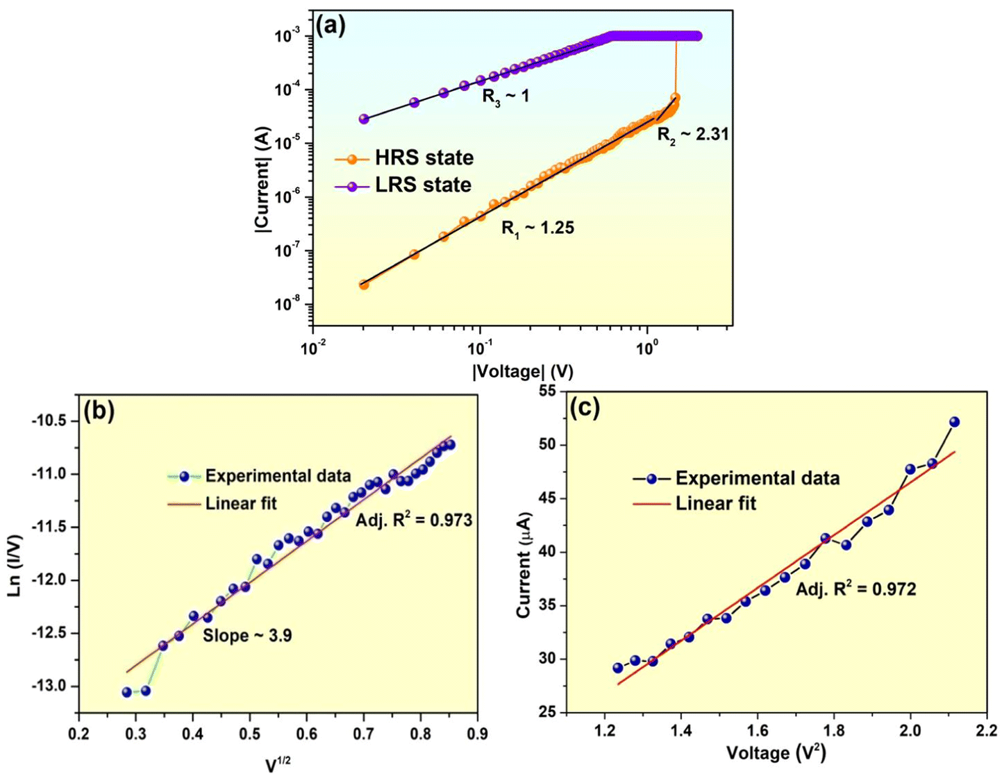
Several conduction mechanisms and techniques, including as space charge limited conduction (SCLC), oxidation-reduction, ohmic behaviour electron tunneling, hopping and trapping–detrapping have been found in general.83–89 In order to understand the conduction mechanism further, we have plotted the I–V curve in log–log scale. Corresponding curve is shown in Fig. 6a. A close look to the curve showed that the value of slope in lower voltage region (regime-1) is 1.25, which indicates the conduction may be due to the thermally generated electrons. In regime-2 value of the slope is 2.31, which clearly indicates the trap controlled space charge limited conduction. In order to have deep insight into these two regimes we have re-plotted regime-1 as ln(I/V) vs. V1/2 and fitted linearly. Fitted result showed adj. R2 value is 0.973, which clearly indicates the conduction in low voltage region (regime-1) is mainly Poole–Frenkel emission. Corresponding plot is shown in Fig. 6b. We have also re-plotted regime-2 as I vs. V2 and fitted linearly shown in Fig. 6c. From the fitted result we have found that adj. R2 = 0.972, i.e., the charge transport in regime 2 supports the electron injected trap controlled SCLC.90,91 When the applied voltage exceeds the operating voltage (1.47 V), the device switches from OFF state to ON state. In the ON state (Fig. 6a), the current conduction is ohmic (regime-3).
 | ||
| Fig. 6 (a) I–V curves in a log–log scale for the device 4; (b) fitting results in the low-voltage region of HRS with the ln(I/V) vs. V1/2 relationship; (c) the plot of I vs. V2 (Child's law region) for the high-slope part of log–log graph. | ||
In order to have better understanding of the conduction mechanism, we have performed heat treatment to the prepared device from 303 K to 353 K with an interval of 10 K. We have performed four set of independent measurement for each temperature. Corresponding threshold voltage, LRS and HRS are shown in Fig. 7a and b respectively. These box plots showing average value with their mean and maximum–minimum values corresponding to the four set of measurements. Almost reproducible switching characteristics have been observed for all the selected temperatures. It has been found that, threshold voltage of the observed devices decreases with increasing temperature (Fig. 7a). As indicated in Fig. 7b, it has been observed that the LRS of the device decreases with rising temperature, which clearly rules out the possibility of formation of metallic filament.31 But it can be inferred that the conduction channel may possibly be due to trapping–detrapping in the active layer of the device.92,93 Also observed decrease in HRS values with temperature (Fig. 7b) suggested active layer posses insulating or semiconducting behavior.94 To have a deeper insight into the conduction mechanism, we have plotted ln(I/V) vs.(1/kT) for different read voltages shown in Fig. 7c. Slope of the corresponding curves gives us the idea about activation energy (Ea).55,56,67 We have analyzed and found activation energy (Ea) for read voltages 0.1, 0.3, 0.5, 0.7 and 0.9 V are 0.60 eV, 0.54 eV, 0.50 eV, 0.42 eV and 0.38 eV respectively. From the plot of activation energy versus square root of V it is observed that the value of Ea decreases with the increasing voltage (Fig. 7d). This result clearly indicates that the depth of the trap inside the active material decreases with the increasing voltages.95 In this regard, information about trap energy is also very important. In order to get an idea about trap energy we have extrapolated the curve of Ea vs. V(1/2) to a zero bias voltage and it is found to be of the order of 0.72 eV.
 | ||
| Fig. 7 (a) Variation of threshold voltage with increasing temperature. (b) Variation of HRS and LRS with the increasing temperature. (c) ln(I/V) vs. (1/kT) plot for the device 4 at read voltages 0.1, 0.3, 0.5, 0.7 and 0.9. (d) Activation energy Ea vs. V(1/2) plot for device 4 to extract the trap energy from the intersection on the Y-axis at zero bias voltage. | ||
In order to have better understanding with the observed data we have illustrated the conduction mechanism with the help of schematic diagram as shown in Fig. 8. At low voltage regime, the traps are unoccupied (Fig. 8a). In this regime, the current conduction is mainly due to thermally generated electrons (regime-1, Fig. 6a). With increase in applied voltage, the traps begin to be filled up by charges transferring from ITO to the active layer (Fig. 8b). High density of traps presents in the active layer lead the charge trapping process. The charge trapping process result in the SCLC model (regime-2, Fig. 6a).96,97 Charge accumulation in traps increases with the applied voltage. This process results higher electron concentration in the active layers of the device. When the applied voltage approaches to the operating voltage, injected carriers in the active layers increase exponentially and all the traps are completely filled (Fig. 8c). Conductive paths are formed in the active layer due to the higher electron concentration. The formation of conductive paths switches the device from OFF state to ON state. Due to accumulation of charges in the active layer, an internal electrical field is formed across the Au/Indole2-SA/ITO device.96 When the power is turned off, the trapped charges are not discharged because the Indole2 & SA around the traps is insulator.25 When a reverse bias is applied to the device, a mass of trapped charges are still reserved in the traps. So the high electron concentration retains in the active layer. This process prevents the rapture of conductive path (Fig. 8d). This is because the internal electrical field associated with the space charge layer in the active layer is high enough to oppose the applied electric field.25 Thus, charges in the traps are difficult to be neutralized or de-trapped due to the protection of the internal electric field. Consequently, the device exhibits WORM memory behavior.
 | ||
| Fig. 8 Schematic illustration of conduction mechanism of the device 4 showing WORM behaviour with configuration Au/Indole2-SA/ITO, where active material are Indole2-SA mixture with Indole2 mole fraction 0.3 (a) the device as prepared condition, (b) the condition at which bias voltage (V) is less than that of threshold voltage (VTh), (c) the device is at threshold voltage, where the conduction channel is formed, (d) the device is in reverse sweep condition and (e) the condition at which bias is removed. | ||
In order to shed further insights into the conduction mechanism, variation of SET (VTh) voltages with the active layer thickness of the devices has been investigated. In order to do that we have prepared four independent devices having active layer thickness of the order of 260, 340, 380 and 450 nm, and their I–V behavior has been investigated. Corresponding results are shown in Fig. S9 of the ESI.† Results reveal that the SET voltages of the prepared device increases with the increasing active layer thickness.98 This suggests that electric field driven mechanism may also play crucial role in the conduction mechanism in addition to the trapping. In order to switch the device from HRS to LRS it is necessary to apply a particular electric field.99 Again for a particular electric field, bias voltage is directly proportional to the thickness of the film.8 Therefore, to achieve a particular electric field, higher bias voltage is required for the device having higher active layer thickness.
On the other hand with increase in thickness of the active layer, number of trap centers due to SA network also increased. This may trap higher number of charge carriers. Therefore, higher bias voltage is required to fill up all the traps and to form a continuous conduction channel between two electrodes resulting larger threshold voltage.
Conclusion
In summary, both volatile threshold as well as non-volatile WORM memory devices was fabricated employing Indole2 molecules and its mixture with SA. Au/Indole2/ITO and Au/Indole2–SA/ITO devices with Indole2 mole fractions 0.5 and 0.8 showed volatile threshold switching with device stability greater than two months and having optimum memory window. The Au/Indole2–SA/ITO device with Indole2 mole fraction 0.3 showed non-volatile switching behavior suitable for WORM applications. Trap controlled SCLC was the key behind the observed bias induced switching of the devices between two resistance states. Trap centers due to SA network in the active layer of the device may be responsible for the formation of permanent conducting filament in between two electrodes leading to the non-volatile behavior of the device. Calculated trap energy was of the order of 0.72 eV. In case of volatile switching devices due to lack of sufficient traps within the active layer, de-trapping may occur under reverse sweep once the device is switched to its ON state under a particular bias voltage. Observed non-volatile WORM memory device showed very good device stability (>285 days), memory window (∼6.69 × 10²), endurance 210 times, excellent retention time (6.8 × 10⁴ s) and device yield of the order of 78.5%. Series of investigations employing tetraindolyl derivatives revealed that indolyl based molecules may be a suitable candidate for various types of memory applications like RRAM, CRS, threshold as well as WORM memory towards realizing organic electronics.Author contributions
S. A. H. and S. S. designed the work. S. S. performed all experiments. S. S, H. B. and F. Y. R. analyze the data. S. M. synthesized the material. S. A. H. and S. S. wrote the manuscript with input from S. M. and D. B.Conflicts of interest
There are no conflicts to declare.Acknowledgements
SAH is grateful to DST, for financial support to carry out this research work through DST, Govt. of India project ref. no. CRG/2021/004073. The authors are also grateful to UGC, Govt. of India for financial support to carry out this research work through financial assistance under UGC – SAP program 2016 (F.530/23/DRS-I/2018 (SAP-I)). The authors acknowledge the central instrumentation centre (CIC), Tripura University for providing FESEM facility.Notes and references
- M. Lanza, F. Palumbo, Y. Shi, F. Aguirre, S. Boyeras, B. Yuan, E. Yalon, E. Moreno, T. Wu and J. B. Roldan, Adv. Electron. Mater., 2022, 8, 2100580 CrossRef CAS.
- N. Ilyas, J. Wang, C. Li, H. Fu, D. Li, X. Jiang, D. Gu, Y. Jiang and W. Li, J. Mater. Sci. Technol., 2022, 97, 254–263 CrossRef CAS.
- I. Oh, J. Pyo and S. Kim, Nanomaterials, 2022, 12, 2185 CrossRef CAS PubMed.
- Y. Li, Z. C. Zhang, J. Li, X.-D. Chen, Y. Kong, F.-D. Wang, G.-X. Zhang, T.-B. Lu and J. Zhang, Nat. Commun., 2022, 13, 4591 CrossRef CAS PubMed.
- M. E. Pam, S. Li, T. Su, Y.-C. Chien, Y. Li, Y. S. Ang and K.-W. Ang, Adv. Mater., 2022, 34, 2202722 CrossRef CAS PubMed.
- S. Chen and I. Valov, Adv. Mater., 2022, 34, 2105022 CrossRef CAS PubMed.
- G. H. Shin, C.-K. Kim, G. S. Bang, J. Y. Kim, B. C. Jang, B. J. Koo, M. H. Woo, Y.-K. Choi and S.-Y. Choi, 2D Mater., 2016, 3, 034002 CrossRef.
- S. Sarkar, H. Banik, S. Suklabaidya, B. Deb, S. Majumdar, P. K. Paul, D. Bhattacharjee and S. A. Hussain, Langmuir, 2021, 37, 4449–4459 CrossRef CAS PubMed.
- S. Sarkar, F. Y. Rahman, H. Banik, S. Majumdar, D. Bhattacharjee and S. A. Hussain, Langmuir, 2022, 38, 9229–9238 CrossRef CAS PubMed.
- K. Y. Cheong, I. A. Tayeb, F. Zhao and J. M. Abdullah, Nanotechnol. Rev., 2021, 10, 680–709 CrossRef CAS.
- S. Gao, X. Yi, J. Shang, G. Liu and R.-W. Li, Chem. Soc. Rev., 2019, 48, 1531–1565 RSC.
- B. Sun, X. Zhang, G. Zhou, P. Li, Y. Zhang, H. Wang, Y. Xia and Y. Zhao, Org. Electron., 2017, 42, 181–186 CrossRef CAS.
- B. Dey, S. Sarkar, H. Banik and S. Arshad Hussain, Mater. Today: Proc., 2021, 46, 6290–6294 CrossRef CAS.
- G. U. Kamble, A. P. Patil, R. K. Kamat, J. H. Kim and T. D. Dongale, ACS Appl. Electron. Mater., 2023, 5, 2454–2481 CrossRef CAS.
- Y. Li, Q. Qian, X. Zhu, Y. Li, M. Zhang, J. Li, C. Ma, H. Li, J. Lu and Q. Zhang, InfoMat, 2020, 2, 995–1033 CrossRef CAS.
- F. M. Simanjuntak, D. Panda, K.-H. Wei and T.-Y. Tseng, Nanoscale Res. Lett., 2016, 11, 368 CrossRef PubMed.
- J. E. Anthony, Angew. Chem., Int. Ed., 2008, 47, 452–483 CrossRef CAS PubMed.
- R. K. Gupta and A. A. Sudhakar, Langmuir, 2019, 35, 2455–2479 CrossRef CAS PubMed.
- Q. Li, L. Lu, C. Zhong, J. Shi, Q. Huang, X. Jin, T. Peng, J. Qin and Z. Li, J. Phys. Chem. B, 2009, 113, 14588–14595 CrossRef CAS PubMed.
- Y. He, C. Guo, B. Sun, J. Quinn and Y. Li, Chem. Commun., 2015, 51, 8093–8096 RSC.
- Y.-Y. Lai, J.-M. Yeh, C.-E. Tsai and Y.-J. Cheng, Eur. J. Org Chem., 2013, 2013, 5076–5084 CrossRef CAS.
- E. Linn, R. Rosezin, C. Kügeler and R. Waser, Nat. Mater., 2010, 9, 403–406 CrossRef CAS PubMed.
- B. Dey, S. Suklabaidya, S. Majumdar, P. K. Paul, D. Bhattacharjee and S. A. Hussain, ChemistrySelect, 2019, 4, 9065–9073 CrossRef CAS.
- A. Bandyopadhyay and A. J. Pal, Chem. Phys. Lett., 2003, 371, 86–90 CrossRef CAS.
- P. Zhang, B. Xu, C. Gao, G. Chen and M. Gao, ACS Appl. Mater. Interfaces, 2016, 8, 30336–30343 CrossRef CAS PubMed.
- D. K. Maiti, S. Debnath, S. M. Nawaz, B. Dey, E. Dinda, D. Roy, S. Ray, A. Mallik and S. A. Hussain, Sci. Rep., 2017, 7, 13308 CrossRef.
- L. Gao, Y. Li, Q. Li, Z. Song and F. Ma, Nanotechnology, 2017, 28, 215201 CrossRef PubMed.
- G. Khurana, P. Misra, N. Kumar, S. Kooriyattil, J. F. Scott and R. S. Katiyar, Nanotechnology, 2015, 27, 015702 CrossRef PubMed.
- W. Banerjee, S. H. Kim, S. Lee, D. Lee and H. Hwang, Adv. Electron. Mater., 2021, 7, 2100022 CrossRef CAS.
- P. Bamola, B. Singh, A. Bhoumik, M. Sharma, C. Dwivedi, M. Singh, G. K. Dalapati and H. Sharma, ACS Appl. Nano Mater., 2020, 3, 10591–10604 CrossRef CAS.
- H. Banik, S. Sarkar, D. Bhattacharjee and S. A. Hussain, ACS Appl. Electron. Mater., 2021, 3, 5248–5256 CrossRef CAS.
- M.-L. Wu, Y.-H. Wu, C.-C. Lin and L.-L. Chen, Appl. Phys. Lett., 2012, 101, 163503 CrossRef.
- W. Banerjee, A. Kashir and S. Kamba, Small, 2022, 18, 2107575 CrossRef CAS PubMed.
- S. Sarkar, B. Deb, B. Dey, S. Suklabaidya, S. Chakraborty, D. Bhattacharjee, S. Majumdar, Y. Suzuki, J. Kawamata and S. A. Hussain, J. Phys. Chem. Solids, 2020, 144, 109487 CrossRef CAS.
- C. Mahata and S. Kim, Ceram. Int., 2021, 47, 1199–1207 CrossRef CAS.
- S. A. Hussain and S. Chakraborty, in Clay-Polymer Nanocomposites, Elsevier, 2017, pp. 273–305 Search PubMed.
- S. A. Hussain, B. Dey, D. Bhattacharjee and N. Mehta, Heliyon, 2018, 4, e01038 CrossRef PubMed.
- W. Wang, A. Bricalli, M. Laudato, E. Ambrosi, E. Covi and D. Ielmini, 2018 IEEE International Electron Devices Meeting (IEDM), 2018, pp. 40.3.1–40.3.4 Search PubMed.
- S. H. Chang, J. S. Lee, S. C. Chae, S. B. Lee, C. Liu, B. Kahng, D.-W. Kim and T. W. Noh, Phys. Rev. Lett., 2009, 102, 026801 CrossRef CAS PubMed.
- D. P. Sahu, K. Park, J. Han and T.-S. Yoon, APL Mater., 2022, 10, 051111 CrossRef CAS.
- H. Sun, Q. Liu, C. Li, S. Long, H. Lv, C. Bi, Z. Huo, L. Li and M. Liu, Adv. Funct. Mater., 2014, 24, 5679–5686 CrossRef CAS.
- J. Pyo, S.-J. Woo, K. Lee and S. Kim, Metals, 2021, 11, 1605 CrossRef CAS.
- W. Banerjee, S. H. Kim, S. Lee, S. Lee, D. Lee and H. Hwang, Adv. Funct. Mater., 2021, 31, 2104054 CrossRef CAS.
- D. Harshini, V. M. Angela, P. Devibala, P. M. Imran, N. S. P. Bhuvanesh and S. Nagarajan, ACS Appl. Electron. Mater., 2022, 4, 4383–4395 CrossRef CAS.
- W.-C. Jhang and C.-C. Hsu, IEEE Trans. Electron Devices, 2022, 69, 4914–4919 CAS.
- A. Mehonic, S. Cueff, M. Wojdak, S. Hudziak, O. Jambois, C. Labbé, B. Garrido, R. Rizk and A. J. Kenyon, J. Appl. Phys., 2012, 111, 074507 CrossRef.
- W. Banerjee, Electronics, 2020, 9, 1029 CrossRef CAS.
- A. Kalantarian, G. Bersuker, D. C. Gilmer, D. Veksler, B. Butcher, A. Padovani, O. Pirrotta, L. Larcher, R. Geer, Y. Nishi and P. Kirsch, IEEE International Reliability Physics Symposium (IRPS), 2012, pp. 6C.4.1–6C.4.5 Search PubMed.
- K. Skaja, M. Andrä, V. Rana, R. Waser, R. Dittmann and C. Baeumer, Sci. Rep., 2018, 8, 1–7 CAS.
- C. Baeumer, R. Valenta, C. Schmitz, A. Locatelli, T. O. Menteş, S. P. Rogers, A. Sala, N. Raab, S. Nemsak, M. Shim, C. M. Schneider, S. Menzel, R. Waser and R. Dittmann, ACS Nano, 2017, 11, 6921–6929 CrossRef CAS PubMed.
- J.-Y. Choi, J. Lee, J. Jeon, J. Im, J. Jang, S.-W. Jin, H. Joung, H.-C. Yu, K.-N. Nam, H.-J. Park, D.-M. Kim, I.-H. Song, J. Yang, S. Cho and C.-M. Chung, Polym. Chem., 2020, 11, 7685–7695 RSC.
- Y. Kuwabara, H. Ogawa, H. Inada, N. Noma and Y. Shirota, Adv. Mater., 1994, 6, 677–679 CrossRef CAS.
- H. Tsuji, K. Sato, Y. Sato and E. Nakamura, J. Mater. Chem., 2009, 19, 3364–3366 RSC.
- K. Kaushlendra, P. Kumar, D. Arora, B. Ranjan and D. Kaur, Ceram. Int., 2023, 49, 9543–9550 CrossRef CAS.
- W. Li, H. Zhu, T. Sun, W. Qu, X. Fan, Z. Gao, W. Shi and B. Wei, J. Phys. Chem. C, 2022, 126, 12897–12905 CrossRef CAS.
- L. Yan, L. Ruan, F. Luo, J. Tong, C. Sun, Y. Zheng, X. Han, Y. Zhang and X. Zhang, Vacuum, 2022, 198, 110862 CrossRef CAS.
- J. Li, C. Yang, Y. Chen and W.-Y. Lai, New J. Chem., 2016, 40, 8886–8891 RSC.
- N. Jia, J. Guo, G. Tian, S. Qi, X. Wang and D. Wu, Dyes Pigm., 2017, 146, 1–6 CrossRef CAS.
- V. M. Angela, D. Harshini, A. Anjali, P. M. Imran, N. S. P. Bhuvanesh and S. Nagarajan, Chem. –Eur. J., 2023, 29, e202202569 CrossRef CAS PubMed.
- Y. Ji, M. Choe, B. Cho, S. Song, J. Yoon, H. C. Ko and T. Lee, Nanotechnology, 2012, 23, 105202 CrossRef PubMed.
- J.-H. Tang, T.-G. Sun, J.-Y. Shao, Z.-L. Gong and Y.-W. Zhong, Chem. Commun., 2017, 53, 11925–11928 RSC.
- J.-Y. Lam, G.-W. Jang, C.-J. Huang, S.-H. Tung and W.-C. Chen, ACS Sustain. Chem. Eng., 2020, 8, 5100–5106 CrossRef CAS.
- Configurable Resistive Switching between Memory and Threshold Characteristics for Protein-Based Devices – Wang – 2015 – Advanced Functional Materials, Wiley Online Library, https://onlinelibrary.wiley.com/doi/full/10.1002/adfm.201501389, accessed January 18, 2023 Search PubMed.
- B. Qu, Q. Lin, T. Wan, H. Du, N. Chen, X. Lin and D. Chu, J. Phys. D: Appl. Phys., 2017, 50, 315105 CrossRef.
- H.-C. Hsieh, N. Wu, T.-H. Chuang, W.-Y. Lee, J.-Y. Chen and W.-C. Chen, ACS Appl. Polym. Mater., 2020, 2, 2469–2476 CrossRef CAS.
- W. Wu, S.-T. Han, S. Venkatesh, Q. Sun, H. Peng, Y. Zhou, C. Yeung, R. K. Li and V. A. L. Roy, Org. Electron., 2018, 59, 382–388 CrossRef CAS.
- S. Chakraborty, D. Bhattacharjee and S. A. Hussain, Appl. Phys. A, 2013, 111, 1037–1043 CrossRef CAS.
- S. A. Hussain, S. Deb and D. Bhattacharjee, J. Lumin., 2005, 114, 197–206 CrossRef CAS.
- S. Suklabaidya, S. Chakraborty, S. Sarkar, R. Paul, H. Banik, A. Chakraborty, D. Bhattacharjee, S. Majumdar and S. A. Hussain, J. Phys. Chem. C, 2021, 125, 15976–15986 CrossRef CAS.
- P. Debnath, S. Chakraborty, S. Deb, J. Nath, D. Bhattacharjee and S. A. Hussain, J. Phys. Chem. C, 2015, 119, 9429–9441 CrossRef CAS.
- M. Jurak, J. Phys. Chem. B, 2013, 117, 3496–3502 CrossRef CAS PubMed.
- S. Scheiner, T. Kar and J. Pattanayak, J. Am. Chem. Soc., 2002, 124, 13257–13264 CrossRef CAS PubMed.
- M. Levitt and M. F. Perutz, J. Mol. Biol., 1988, 201, 751–754 CrossRef CAS PubMed.
- E. L. Correia, N. Brown, A. Ervin, D. V. Papavassiliou and S. Razavi, Langmuir, 2022, 38, 7179–7189 CrossRef CAS PubMed.
- Y. Zhu, F. Zhang, C. Zhang, L. Yang, G. Fan, Y. Xu, B. Sun and X. Li, Sci. Rep., 2018, 8, 8612 CrossRef PubMed.
- B. Dey, S. Chakraborty, S. Chakraborty, D. Bhattacharjee, A. Khan and S. A. Hussain, Org. Electron., 2018, 55, 50–62 CrossRef CAS.
- W. Daear, M. Mahadeo and E. J. Prenner, Biochim. Biophys. Acta, Biomembr., 2017, 1859, 1749–1766 CrossRef CAS PubMed.
- S. U. Sharath, M. J. Joseph, S. Vogel, E. Hildebrandt, P. Komissinskiy, J. Kurian, T. Schroeder and L. Alff, Appl. Phys. Lett., 2016, 109, 173503 CrossRef.
- M. Asif and A. Kumar, Mater. Today Electron., 2022, 1, 100004 CrossRef.
- H. Wang, Y. Du, Y. Li, B. Zhu, W. R. Leow, Y. Li, J. Pan, T. Wu and X. Chen, Adv. Funct. Mater., 2015, 25, 3825–3831 CrossRef CAS.
- A. K. Shringi, A. Betal, S. Sahu and M. Kumar, J. Mater. Sci.: Mater. Electron., 2022, 33, 12490–12499 CrossRef CAS.
- Q. Cao, L. Xiong, X. Yuan, P. Li, J. Wu, H. Bi and J. Zhang, Appl. Phys. Lett., 2022, 120, 232105 CrossRef CAS.
- Z. W. Dlamini, S. Vallabhapurapu, O. A. Daramola, P. F. Tseki, R. W. M. Krause, X. Siwe-Noundou, T. S. Mahule and S. V. Vallabhapurapu, Iran. J. Sci. Technol., Trans. A: Sci., 2022, 46, 709–716 CrossRef.
- M. M. Chang, D. Y. Guo, X. L. Zhong, F. B. Zhang and J. B. Wang, J. Appl. Phys., 2022, 132, 123105 CrossRef CAS.
- S. Kunwar, C. B. Somodi, R. A. Lalk, B. X. Rutherford, Z. Corey, P. Roy, D. Zhang, M. Hellenbrand, M. Xiao, J. L. MacManus-Driscoll, Q. Jia, H. Wang, J. Joshua Yang, W. Nie and A. Chen, Adv. Electron. Mater., 2023, 9, 2200816 CrossRef CAS.
- L. Doowon, B. Dongjoo, K. Sungho and H.-D. Kim, Ceram. Int., 2022, 48, 20478–20484 CrossRef CAS.
- P.-K. Zhou, X.-L. Lin, H.-L. Yang, B.-J. Chen, H.-H. Li, Z.-R. Chen and S.-T. Zheng, J. Alloys Compd., 2022, 925, 166783 CrossRef CAS.
- A. Sharma, M. Faraz and N. Khare, Eur. Phys. J. Plus, 2022, 137, 1197 CrossRef CAS.
- N. Alam, S. Majumder, S. J. Ray and D. Sarma, Langmuir, 2022, 38, 10601–10610 CrossRef CAS PubMed.
- X. Xiang, J. Rao, C. Lim, Q. Huang, S. Zhao, Z. Fan, J. W. Han and Y. Chen, ACS Appl. Electron. Mater., 2022, 4, 2729–2738 CrossRef CAS.
- N. C. Das, M. Kim, J. R. Rani, S.-M. Hong and J.-H. Jang, Nanoscale, 2022, 14, 3738–3747 RSC.
- Y. Zhu, M. Zhao, Y. Zhang, T. Zhang and H. Zhou, Appl. Phys. Lett., 2022, 120, 103504 CrossRef CAS.
- X. Lai, B. Liu, Y. Wang and L. Zhang, J. Alloys Compd., 2022, 890, 161851 CrossRef CAS.
- S. He, A. Hao, N. Qin and D. Bao, RSC Adv., 2017, 7, 38757–38764 RSC.
- G. Zhou, B. Sun, X. Hu, L. Sun, Z. Zou, B. Xiao, W. Qiu, B. Wu, J. Li, J. Han, L. Liao, C. Xu, G. Xiao, L. Xiao, J. Cheng, S. Zheng, L. Wang, Q. Song and S. Duan, Advanced Science, 2021, 8, 2003765 CrossRef CAS.
- J. Liu, Z. Zeng, X. Cao, G. Lu, L.-H. Wang, Q.-L. Fan, W. Huang and H. Zhang, Small, 2012, 8, 3517–3522 CrossRef CAS PubMed.
- P. Zhang, C. Gao, B. Xu, L. Qi, C. Jiang, M. Gao and D. Xue, Small, 2016, 12, 2077–2084 CrossRef CAS PubMed.
- L. Liu, J. Dong, J. Liu, Q. Liang, Y. Song, W. Li, S. Lei and W. Hu, Small Struct., 2021, 2, 2000077 CrossRef CAS.
- S. Duhalde, M. Villafuerte, G. Juárez and S. P. Heluani, Phys. B, 2004, 354, 11–15 CrossRef CAS.
Footnote |
| † Electronic supplementary information (ESI) available. See DOI: https://doi.org/10.1039/d3ra03869f |
| This journal is © The Royal Society of Chemistry 2023 |