
 Open Access Article
 This Open Access Article is licensed under a Creative Commons Attribution-Non Commercial 3.0 Unported Licence
Thermoelectric and power generation of 2D structured pieces of graphene–nanodiamonds nanocomposite†
Ibrahim K. Alsulami*abcd,
Shittu Abdullahi *ae,
Ahmed Alshahrieac and
Numan Salah*bc
*ae,
Ahmed Alshahrieac and
Numan Salah*bc
aPhysics Department, Faculty of Science, King Abdulaziz University, Jeddah 21589, Saudi Arabia
bK. A. CARE Energy Research and Innovation Center, King Abdulaziz University, Jeddah 21589, Saudi Arabia
cCentre of Nanotechnology, King Abdulaziz University, Jeddah 21589, Saudi Arabia
dFaculty of Science, King Abdulaziz Military Academy, Riyadh, Saudi Arabia
eDepartment of Physics, Faculty of Science, Gombe State University, P.M.B. 127, Gombe, Nigeria
First published on 1st September 2023
Abstract
Recently, the ultrafine 2D structured nanocomposite of graphene (Gr)–nanodiamonds (NDs) produced by a microwave-assisted chemical route was found to have attractive structural properties. This new 2D structured nanocomposite may be employed for a wide spectrum of applications including thermoelectricity (TE) applications. It is well established that TE materials should be highly effective to be used for designing operative devices for powering or cooling small devices. To fulfill such an objective, the functional TE material should possess a high-power factor and low thermal conductivity. In this study, NDs were successfully integrated into Gr with a magnificent structural alteration to the Gr layers/sheets. This structural modification was found to impact the TE final outcome above and below room temperature (RT). The obtained results showed that at 215 K the power factor value was increased from 4 μW m−1 K−2 for the pure Gr to ∼20 μW m−1 K−2 for the Gr–NDs nanocomposite. At higher T, e.g. 365 K, these values slightly decreased, but with clear superiority for the Gr–NDs nanocomposite. The thermal conductivity of the Gr–NDs nanocomposite was significantly reduced to ∼12% of that of the pure Gr, which could reflect a significant enhancement in the value of the figure of merit by >45 times. Furthermore, the output power generated by a single small leg module made of the Gr–NDs nanocomposite was measured and found to be measurable. The obtained values are still relatively low for practical application, but this newly produced material has great potential to be further developed for TE applications.
Introduction
Thermoelectric (TE) materials contain temperature gradients that directly convert heat to electricity. While thermoelectricity does not generate deleterious by-products and, therefore, offers potential for next-generation green energy techniques, thermoelectric devices ultimately have limited commercial applications due to their limited thermoelectric property.1 The ratio of the voltage developed to the temperature gradient (DV/DT) is related to an intrinsic property of the materials called the Seebeck coefficient or the thermopower. The Seebeck coefficient is very low for metals (only a few mV K−1) and much larger for semiconductors (typically a few 100 mV K−1).2,3 The potential of the material for TE applications is determined in large part by a measure of the material's dimensionless figure of merit (zT), which is expressed as S2σT/κ where S is the Seebeck coefficient, σ is electric conductivity, κ is thermal conductivity, and T is the absolute temperature.4 This figure shows that for effective thermoelectricity it is essential for the TE material to have low thermal conductivity and high electrical conductivity and Seebeck coefficient.4,5 The power factor is typically optimized as a function of carrier concentration (typically around 1019 carriers per cm3), through doping, to give the largest zT.6 High mobility carriers are most desirable in order to have the highest electrical conductivity. Semiconductors have been primarily the materials of choice for thermoelectric applications. The zT for a single material is somewhat incomplete since an array of TE couples is utilized in a device or module.7–9 This has led to extensive research work to enhance the TE performance of a variety of materials.1Low-temperature TE materials are still rarely developed. Most of the developed materials were applied practically at a temperature that was only far above RT. Bi2Te3-based compounds are applicable to generate electricity at low temperatures.10 However, the TE properties using these compounds at low temperatures are rarely reported in the literature. Afterward, some efforts were made to develop other low-temperature TE materials such as BiSb alloys,11 Ta4SiTe4 crystal in its one-dimensional form,12 Ce(Ni1−xCux)2Si2 and CeNi2(Si1−yGey)2,13 CoSi and Co1−xMxSi.14 While continuous theoretical research regarding TE properties of graphene predicts that the dimensionless zT could be greater than four,15,16 experimental results found that zT values equaled less than one due to low graphene thermo-power and high thermal conductivity. Thus, efforts should be made to reduce thermal conductivity to enhance the zT for graphene-based TE devices.17
Carbon nanomaterials, such as carbon nanotube (CNT), carbon dot, and graphene, have revealed excellent properties as TE materials due to their lightweight, nontoxicity, and ultrahigh electrical conductivity.10 However, their high thermal conductivities (∼3000 W m−1 K−1) prevent them from achieving the promised high TE performance, so various methods of nanostructuring (such as nano meshes or nanoribbons) are carefully designed to reduce the value of κ.18 The unique structure of graphene is made up of carbon atoms covalently bonded to three other carbon atoms, resembling a honeycomb lattice.4,19 It has demonstrated its potential to be an effective material for numerous applications. However, its characteristics and promise as a useful material in several practical applications are constrained by poor dispersion caused by the strong π–π stacking interactions between its layers.20–22 Nanodiamonds (NDs), which gained much interest because of their small size, large surface area, high strength, stiffness, and low weight, could have the ability to minimize π–π stacking interactions between Gr layers.20 They have moreover shown to be an excellent choice when used as a reinforcement for Gr exfoliation.23 In addition, doped NDs have demonstrated thermoelectric transport properties using a set of eight substrate-free boron-doped nanocrystalline diamond foils.24 Some previous studies reported mixed particles of NDs with Gr layers as a composite nanostructure for several applications, such as supercapacitor electrodes, devices, and batteries.20
Recently, the ultrafine two-dimensional (2D) structured nanocomposite of graphene (Gr)–nanodiamonds (NDs) produced by the microwave irradiation method was found to have attractive structural properties.23 This structure might be quite useful for energy harvesting from waste or solar heat as a TE nanomaterial. It is well known that the TE material should possess a high-power factor and low thermal conductivity.25,26 These factors were providentially observed in the produced Gr–NDs nanocomposite in its compact pellet form. The objectives of this scientific report are based on firstly, incorporating the NDs into Gr nanosheets and investigating the structural alterations occurring within the Gr nanosheets. These modifications were analyzed by several microscopic techniques including Scanning Electron Microscopy (SEM) and Transmitting Electron Microscopy (TEM). Secondly, the thermo-electrical properties of the produced Gr–NDs nanocomposite in compact pellet form were measured within the temperature range 213–365 K. A good improvement in the TE performance was observed compared to that of the pure graphene. Finally, the output power generated by a single-leg rectangle-shaped module was also measured and found to be measurable in the case of the Gr–NDs nanocomposite. These results were discussed in more detail. The main significance of this study is targeting thermo-electrical properties below room temperature which is rarely studied in other literature.
Experimental details
Materials
The Gr–NDs nanocomposite was synthesized as reported previously using the microwave irradiation system of Milestone, Italy.23 The initial materials employed in this study were used with no further modifications or purifications. The 99% pure graphene (of 1–5 layers) was purchased from AD Nanotech, India, and the ≥98% pure nanodiamonds, with sizes ranging from ∼5–10 nm, were purchased from Carbon Solutions Group, USA. These raw versions of graphene and nanodiamonds were named Gr and NDs, respectively. The 99.99% pure dimethylformamide (DMF) and xylene solvents were likewise supplied from Sigma Aldrich, Germany. The ratio of the nanodiamond to that of graphene in the as-fabricated nanocomposite.Samples characterizations and TE measurement
A field emission scanning electron microscope (FESEM, model JEM 6700F, JEOL, Japan) captured top and lateral imaging of both the Gr–NDs nanocomposite and original pure Gr-rec pellets. A transmission electron microscopy (TEM) image was also taken for the produced nanocomposite using the TEM system model JEM 2100F, JEOL. The formed pellets of 13 mm diameter and 2 mm thickness or of the rectangular shaped legs (of 2 × 6 × 10 mm) were fabricated using a hydraulic press machine by applying around 15 tons to produce highly dense pellets/cubes. Although the ratios of Gr and NDs were 95 and 5%, respectively in the fabricated Gr–NDs nanocomposites, as shown in Fig. S1 (ESI†). The electrical conductivity and Seebeck coefficient were recorded at a temperature gradient of 50 K min−1 and a heating rate of 5 K min−1. These measurements were conducted within the temperature range of 215–365 K by using the HCS 10 system produced by Linseis, Germany. The measurements were performed in a direction parallel to the surface of the pellets. Additionally, the HCS 10 system has been used to record the carrier concentrations and Hall mobility. Finally, a laser flash method in LFA-1000 (Linseis, Germany) was used to determine the in-plane thermal conductivity of both the Gr and Gr–NDs nanocomposite pellets. In this measurement, a graphite sample holder designed for in-plane measurement was used under a vacuum atmosphere, and the heating rate was set at 10 K min−1.Power generation measurement
The output power generated by the Gr and Gr–NDs nanocomposite was conducted using a single leg of a rectangle-shaped module (dimensions = 2 × 6 × 10 mm). The leg was fixed perpendicularly using a stand made of a ceramic plate, while an aluminum sheet of a thickness of around 0.1 mm was used to attach both sides of the TE leg to the measurement systems. Silver (Ag) electrodes on either side of the TE leg measurement system were also used to facilitate charge transport. An infrared temperature gun was used to measure the temperatures on both sides of the leg. The power measurement was repeated several times to ensure the material was stable and reusable.Results and discussions
Structural and morphological properties
In the research,23 it is reported that the experimental parameters for producing the Gr–NDs nanocomposite were varied, including removing one solvent, changing the reaction time, and removing the NDs themselves, to control the Gr sheet size, shape, and morphology. These alterations resulted in no changes in Gr size, shape, or morphology. Consequently, this study has chosen to apply the same methodology as the previous research.23 The outcomes of this work were applied to evaluate the TE performance of the produced Gr–NDs nanocomposite.The morphology of the resulting Gr–NDs nanocomposite was again studied to confirm the earlier reported result.23 The pure Gr and pure NDs samples were also studied for their morphology. The obtained results are shown in Fig. 1a and b, respectively. It shows the SEM images of the samples in powder form. Fig. 1c and d, on the other hand, shows the SEM and TEM images of the resulting Gr–NDs nanocomposite formed in a mixture of xylene and DMF through a microwave-assisted method in powder form. A comparison of the different images demonstrates a noteworthy change. Fig. 1a shows a few Gr layers, while the SEM and TEM images in Fig. 1c and d, respectively show tiny slice composite material structures of Gr–NDs with an approximate size dimension within the range of 0.1–0.5 μm in length and 20–300 nm in width making almost 2D structures. The TEM images in Fig. 1d–f, revealed small particles of NDs (∼3 to 8 nm) in diameter attached to the surface of the sliced Gr sheet as a composite material and other unattached Gr nanosheets, this result is consistent with the Raman analysis as sowing in Fig. S2 (ESI†). The SEM and TEM images clearly show that the Gr layers have decreased in size and altered in shape by mixing with ND to form Gr–NDs nanocomposite. The ratio of the nanodiamonds in the as-fabricated nanocomposite same to be closer to that used in the initial stage, which is 5 wt%. One explanation for this result is due to the defects that were created by NDs, which perhaps affected the graphene nucleation and growth stages, and significantly affected the final shape and size of the final product.27
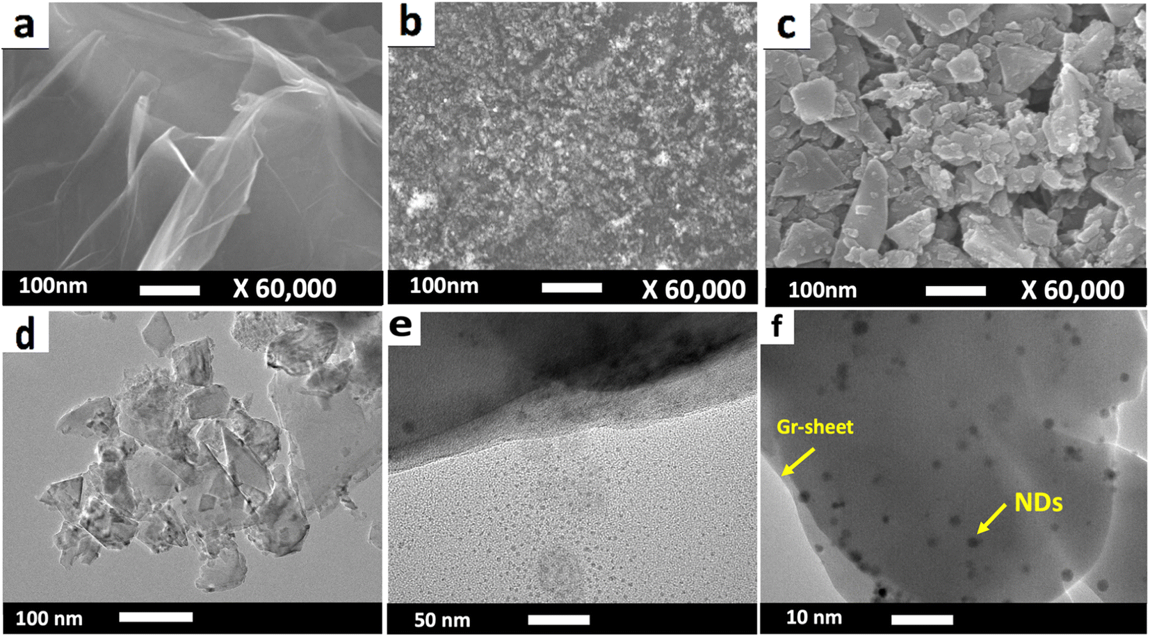 | ||
Fig. 1 SEM images at the same magnification of Gr (a) and NDs (b) powder samples. (c–f) SEM and TEM images of the produced pieces of Gr–NDs formed in xylene and DMF at a ratio 1![[thin space (1/6-em)]](https://www.rsc.org/images/entities/char_2009.gif) :1, under microwave irradiation for 30 min, the concentration of Gr in DMF 50 mg mL−1 the concentration of NDs in xylene 2.5 mg mL−1. :1, under microwave irradiation for 30 min, the concentration of Gr in DMF 50 mg mL−1 the concentration of NDs in xylene 2.5 mg mL−1. | ||
To study the TE properties of the produced Gr–NDs nanocomposite sample and its comparison with those of the pure Gr, they were highly pressed by a hydraulic press to make compact, highly dense pellets. These pellets were studied for their morphologies by the SEM technique. The SEM images presented in Fig. 2a–d show top and cross-section view images for these samples. The top view images of the Gr and Gr–NDs pellets are shown in Fig. 2a and b, while the cross-section images are shown in Fig. 2c and d, respectively. The top view images show pressed layers/sheets of Gr and small sliced pressed sheets of Gr–NDs nanocomposite. The cross-section images show well-pressed sheets of these samples, which are almost in one direction parallel to the pellet surface, but in a zigzagged manner. The sheets of the Gr are much longer than those of the Gr–NDs nanocomposite. According to a statistical analysis performed by SEM, the nanosheets averaged 18.2 nm in thickness (Fig. 2c), however, these nanosheets might still contain sublayers of smaller thickness. Additionally, it is expected that once the NDs have incorporated with the Gr layers, atomic entrapment of NDs will likely occur within Gr, forming lattice structures and causing bi-axially parallel alignment of Gr–NDs nanocomposite.28
 | ||
| Fig. 2 Top view SEM images of (a) Gr and (b) Gr–NDs pellets. The cross-section views of SEM images of Gr and Gr–NDs pellets are also shown in (c) and (d). | ||
Thermoelectric properties
The goal of this study is to address the TE properties of the formed Gr–NDs nanocomposite produced by the microwave irradiation method. The electrical conductivity, σ and Seebeck coefficient, S of the Gr and Gr–NDs nanocomposite pellets were recorded within the temperature range 2015–365 K. The obtained results of these two factors along with the resulting power factor are shown in Fig. 3a–c. The electrical conductivity of the Gr–NDs nanocomposite is found to be higher than that of the pure Gr as shown in Fig. 3a. At 215 K the electrical conductivity of the pure Gr recorded around 18000 S m−1, while by heating to 365 K this value increased to ∼20000 S m−1. Surprisingly, the electrical conductivity of the Gr–NDs nanocomposite was increased by around 10% higher than that of pure Gr. By heating the sample, it shows a similar trend to that of the pure Gr.
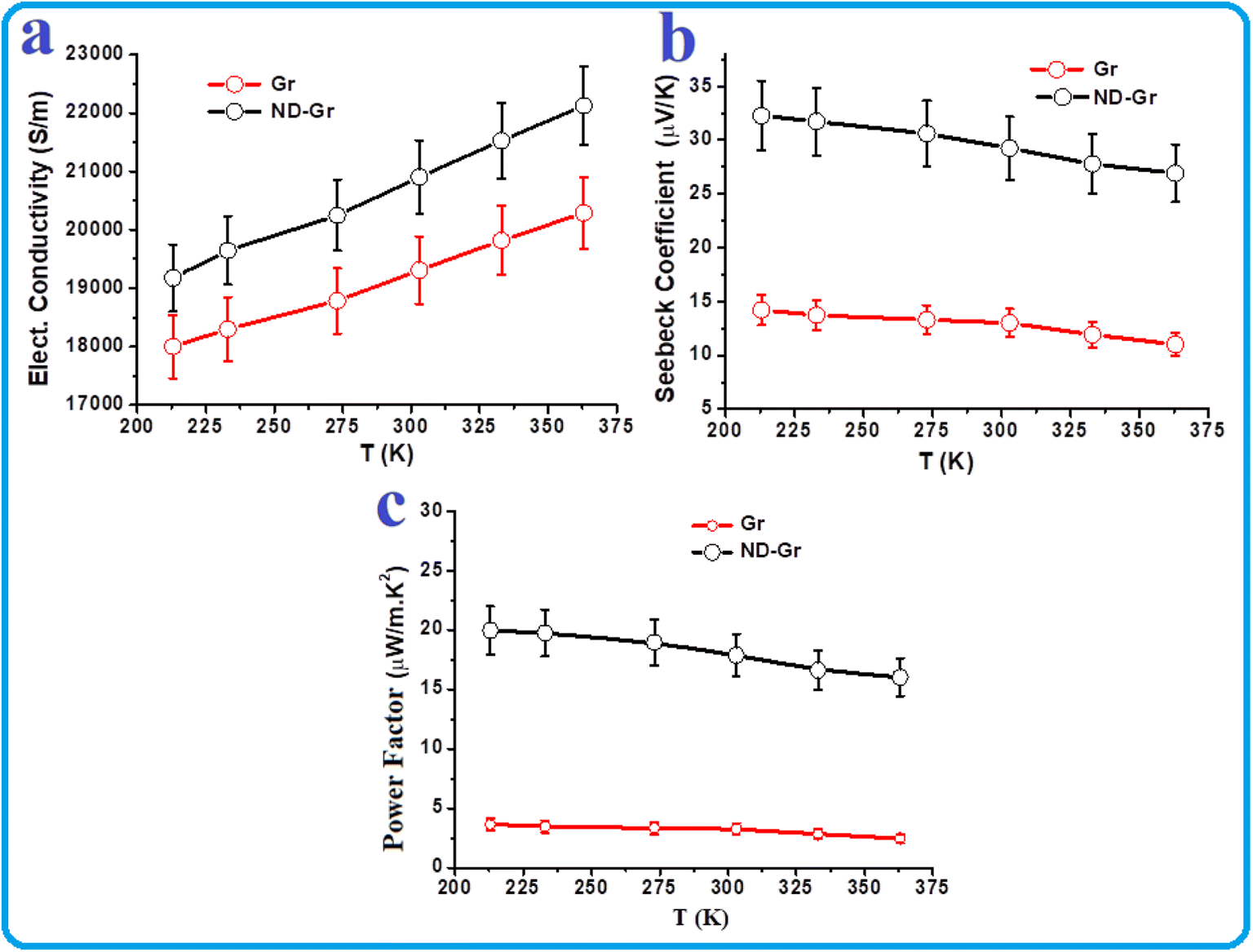 | ||
| Fig. 3 TE performance of the Gr and ND–Gr nanocomposite in the form of compact pellets as the function of temperature: (a) electrical conductivity, (b) seebeck coefficient, and (c) power factor. | ||
The reason behind the observed increases in the electrical conductivity of the Gr–NDs nanocomposite compared to that of pure Gr might be related to the modifications induced in the charge carrier density.29 Formation of extra interfacing sites and charged edges in a matrix of the Gr–NDs nanocomposite might contribute to this enhancement. In addition, diamond nanoparticles with a small size range from (∼3 to 8 nm), might have provided bridges between the exfoliated graphene layers, and created more electron transport paths in the through-direction; as a result, the ratio of in-plane/through-plane electrical conductivity can be increased.30,31 As shown above in Fig. 1b the present Gr–NDs nanocomposite is rich in interfacing sites and most probably charged edges, therefore the density of charge carriers is expected to be increased. Therefore, we in the end get significant improvement in the electrical conductivity. Additionally, the Gr–NDs nanocomposite exhibits anisotropic thermal characteristics (presented in the next paragraphs) almost like pure graphene29,32 with high in-plane thermal conductivity and ultralow through-plane thermal conductivity due to its inherent 2D structure. This 2D structure property of the new Gr–NDs nanocomposite is expected to retain its high electrical conductivity, besides the formation of more charged defects, particularly at the edge of the formed exfoliated sheets that could increase the density of charge carriers, then the electrical conductivity. This will also be discussed in the next paragraphs.
In the case of the Seebeck coefficient, its recorded curves (Fig. 3b) for both the Gr and Gr–NDs nanocomposite have similar trends to those of the electrical conductivity. By this means, the Seebeck value was enhanced in the case of the Gr–NDs nanocomposite. This nanocomposite was found to have a p-type semiconducting property. By heating the samples, the Seebeck values of both samples decreased. At 215 K the Seebeck coefficient values of the pure Gr recorded around 15 μV K−1, while by heating to 365 K this value decreased to ∼12 μV K−1. The Gr–NDs nanocomposite has shown a similar trend but with a significant enhancement of around 50% higher than that of the pure Gr. This might be related to the higher energy-filtering effect.32 As shown in Fig. 2b and d, that there are more interfacing sites and possibly more charged carriers (mainly at the edges) were created in the matrix of the new Gr–NDs nanocomposite. This is expected to enhance both the charge carrier density and the energy filtering sites and their effects, resulting in improving both the electrical conductivity and Seebeck coefficient.
Fig. 3c illustrates the power factor (PF) values as a function of the temperature of both the Gr and Gr–NDs nanocomposite. This factor is equal to S2σ, which provides initial insight into the TE property of a semiconducting material. The PF curve of the Gr–NDs nanocomposite has clear improvement across the specified range of temperatures e.g., 215–365 K, compared to that of the pure Gr. At 215 K the PF value of the pure Gr recorded around 3.5 μW m−1 K−2, while by heating to 365 K this value decreased to ∼2.5 μW m−1 K−2. In the case of the Gr–NDs nanocomposite, its PF recorded values higher by more than 6 times. The recorded values are within the range of 20–17 μW m−1 K−2 corresponds to the temperature range 215–365 K. This significant enhancement is obviously due to the increase in σ and S values mentioned above.
To further elaborate on the observed enhancement in the TE performance of the Gr–NDs nanocomposite, the charge carrier density and the Hall mobility were measured, and the obtained results are presented in Fig. 4a and b, respectively. The charge carrier density in the Gr–NDs nanocomposite is found to be much higher than that of the pure Gr as shown in Fig. 4a. At 215 K the charge carrier density of the pure Gr recorded around 0.9 × 1020 cm−1, while by heating to 365 K this value slightly increased to 1.2 × 1020 cm−1. In the case of the Gr–NDs nanocomposite, the initial value recorded at 215 K is 2.4 × 1020 cm−1, but at 365 K it promptly reached 6 × 1020 cm−1. Compared to pure graphene, the carrier density in the nanocomposite is found to be temperature independent. This independence might be due to the created charges at the edges of the ultrafine 2D sliced pieces of the Gr–NDs nanocomposite. The large increase in the charge carrier density by going from the pure Gr to the Gr–NDs nanocomposite might be related to the same reason. The extra charges created at the edge of the sliced pieces of the Gr–NDs nanocomposite might significantly enhance the charge carrier density.33
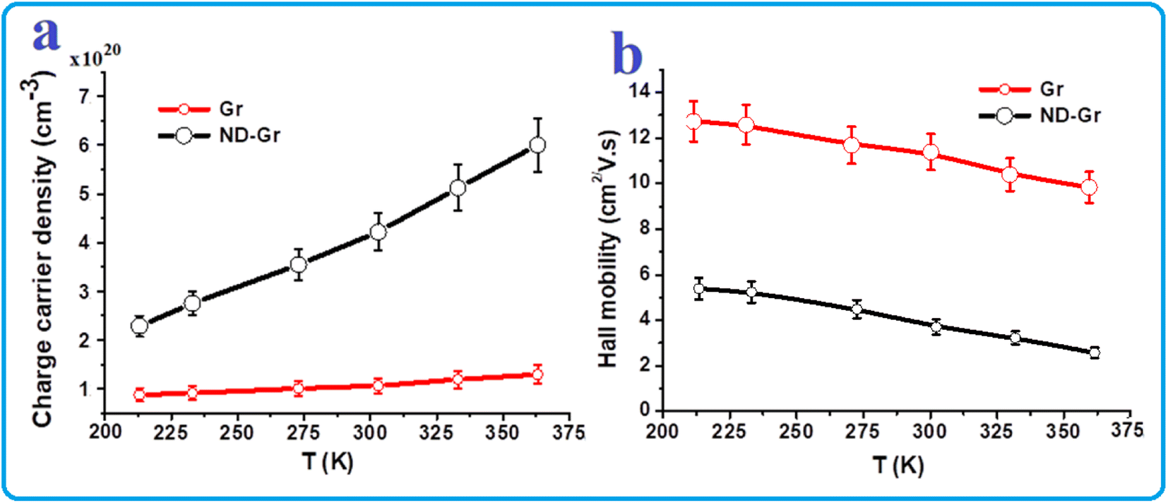 | ||
| Fig. 4 Charge carrier density (a) and Hall mobility (b) versus temperature of the ND–Gr nanocomposite in compact pellet form. The same for the used graphene in pellet form is also shown for comparison. | ||
The Hall mobility results presented in Fig. 4b of both the Gr and Gr–NDs nanocomposite showed an opposite trend to that of the charge carrier density presented in Fig. 4a of both materials. The Hall mobility of the charge carriers of the Gr–NDs nanocomposite is found to be smaller than that of the pure Gr. Both materials in the present work have p-type (electron holes are the major charge carriers) semiconducting properties, as reflected by the positive values of the Seebeck coefficient (Fig. 3b). The excess or increases in the charge carriers are well known to reduce their mobility, particularly if they are electron holes. At 215 K the mobility of the charge carriers of the pure Gr is approximately 12.8 cm2 V−1 s−1, whereas by heating to 365 K this value slightly decreased to ∼10 cm2 V−1 s−1. In the case of the Gr–NDs nanocomposite, the first value recorded at 215 K is 5.5 cm2 V−1 s−1, and at 365 K it decreased to 2.3 cm2 V−1 s−1. However, this decrease in the mobility in the Gr–NDs nanocomposite is not matching the increases in the charge carrier density (smaller), which results in a higher electrical conductivity (Fig. 3a). It is understood that defects can greatly alter the electronic properties of semiconducting materials. The in-plane defects (like vacancy defects) are more prominent in few-layer graphene. It is also well-established that grain-boundary defects are present in graphene. These kinds of defects most probably were increased in the present small pieces of Gr–NDs nanocomposite, which results in decreasing the charge carrier mobility. It is well known that the excess of electron holes can reduce their mobility because this kind of charge carrier is almost delocalized.
Thermal conductivity (κ) has a great impact on the performance of a TE material. The value of κtotal is the sum of lattice thermal conductivity (κl) and electronic thermal conductivity (κe), i.e., κtotal = κp + κe which are created from the phonons and charge carries, respectively. The κe can be calculated using Wiedemann–Franz's law, where the κe = 2.44 × 10⁻⁸σT.37 It is reported that the value of κtotal can be determined for a variety of materials including semiconductors or non-metallic structures.29 The in-plane κtotal, κp, and κe of the present pure Gr and Gr–NDs nanocomposites were recorded in the temperature range 298–373 K and presented in Tables 1 and 2 respectively. The obtained results showed that the κtotal of the pure Gr in its compact form is equal to 1334 W m−1 K−1 at 298 K, this value increased to 1374 W m−1 K−1 by heating to 373 K (Table 1). These values are comparable and in agreement with those reported throughout the literature.34–36 The κe is very small compared to its κtotal, while the κp is closer to the κtotal (Table 1), indicating that the phonons are the major heat carriers in the pressed pellet Gr sample.
| T (K) | Density (g cm−3) | C (J g−1 K−1) | D (cm2 s−1) | κtotal (W m−1 K−1) (±5%) | κp (W m−1 K−1) | κe (W m−1 K−1) | σ (S m−1) | PF (μW m−1 K−2) | zT × 10−5 (±5%) |
|---|---|---|---|---|---|---|---|---|---|
| 298 | 2.10 | 1.113 | 5.708 | 1334.13 | 1333.99 | 0.14 | 19200 |
3.15 | 0.070 |
| 323 | 1.128 | 5.718 | 1354.47 | 1354.32 | 0.15 | 19650 |
3.05 | 0.072 | |
| 348 | 1.155 | 5.719 | 1387.14 | 1386.97 | 0.17 | 20050 |
2.80 | 0.071 | |
| 373 | 1.152 | 5.680 | 1374.10 | 1373.91 | 0.19 | 20450 |
2.50 | 0.068 |
| T (K) | Density (g cm−3) | C (J g−1 K−1) | D (cm2 s−1) | κtotal (W m−1 K−1) (±5%) | κp (W m−1 K−1) | κe (W m−1 K−1) | σ (S m−1) | PF (μW m−1 K−2) | zT × 10−5 (±5%) |
|---|---|---|---|---|---|---|---|---|---|
| 298 | 1.88 | 1.359 | 0.641 | 163.89 | 163.74 | 0.15 | 20800 |
17.90 | 3.25 |
| 323 | 1.401 | 0.655 | 172.52 | 172.35 | 0.17 | 21300 |
17.00 | 3.18 | |
| 348 | 1.462 | 0.660 | 181.40 | 181.21 | 0.19 | 21800 |
16.35 | 3.14 | |
| 373 | 1.502 | 0.672 | 189.76 | 189.56 | 0.20 | 22350 |
15.80 | 3.11 |
The in-plane κtotal, κp, and κe of the Gr–NDs nanocomposites are shown in Table 2. The obtained results showed that the κtotal is equal to 163.89 W m−1 K−1 at 278 K and 189.76 W m−1 K−1 at 373 K. The κe is very small compared to its κtotal, while the κp is closer to the κtotal (Table 2), indicating that the phonons are the major heat carriers in this nanocomposite sample. The reduction in the value of the thermal conductivity here might be attributed to the small average grain size of the Gr–NDs nanocomposite and to the extra interfacing sites. This reduction in the sizes and increases in the interfacing sites leads to higher phonon scattering and thus to a substantial decrease in thermal conductivity. In combination with the grain boundary scattering, there was also a formation of more vacancy defects and voids formed by mixing the NDs within the Gr lattice. This can also increase phonon scattering in these instances.
It can be deduced that pure Gr in isolation has fewer vacancy defects, as well as straight atoms aligned, and arranged, as illustrated in Fig. 2. These core characteristics can cause the facile flow of phonons over a sample range. Gr–NDs nanocomposite, as illustrated in Fig. 2b, suggests a higher number of defects and humps over the sample. As a result of this, the interactions occurring between defects and phonons must be accounted for as the Gr–NDs nanocomposite SEM images portrayed a rough surface at the interface sites. This might increase the chance of forming effective phonon-scattering centers. In addition, the sharpness that these samples recorded could streamline future phonon scattering.
The reduction in thermal conductivity can be considered proof of the effective scattering of phonons at the interfaces of the Gr–NDs nanocomposite. These rough surface characteristics of a Gr–NDs nanocomposite can generate destructive interference. This could prompt better contact thermal resistance, and in turn, greater phonon scattering. Assumptions have been made in this study that every phonon that contacts the rough surface is scattered in all directions and that this effect causes phonon–phonon and electron–phonon interactions. It can in turn be stated that the roughness of the surface imposes a substantial effect on phonon transport.37 It is this prospect that perfectly causes a reduction in phonons as well as a minor effect on the electrons. This introduces a given material structural order on a nanometer scale, whereby it is possible in certain instances to induce phonon scattering without impacting charge carriers. This could justify the innovative proposition of phonon glass-electron crystal materials.38
Tables 1 and 2 assess the figure of merit, zT values of the present pressed pellets of Gr and Gr–NDs nanocomposite. As a result of the relatively low values of PF and the high values of κtotal, the values of zT of pure Gr are considerably low, ranging from 0.07–0.068 × 10⁻⁵. Nevertheless, these values are comparable to those outlined in the literature. Further, because of the attractive structural properties of Gr–NDs nanocomposite, which could reduce thermal conductivity and provide an enhanced power factor, the zT values reached >45 times higher than that of pure Gr. The normalized values of the main factors, which are power factor, PF, thermal conductivity, κ and figure of merit, zT of the Gr–NDs nanocomposite and their comparison with those of pure graphene obtained at RT are plotted in Fig. 5. They clearly show the valuably of the produced Gr–NDs nanocomposite and their TE performance. Although the thermal conductivity is significantly reduced by more than 8 times, it is still high for better TE performance. The results of this study suggest that zT may be increased by further reduction on the value of κtotal possibly by including more modifications on the produced nanocomposites or incorporating them with some conducting polymers like polypyrrole or polyaniline or PEDOT.
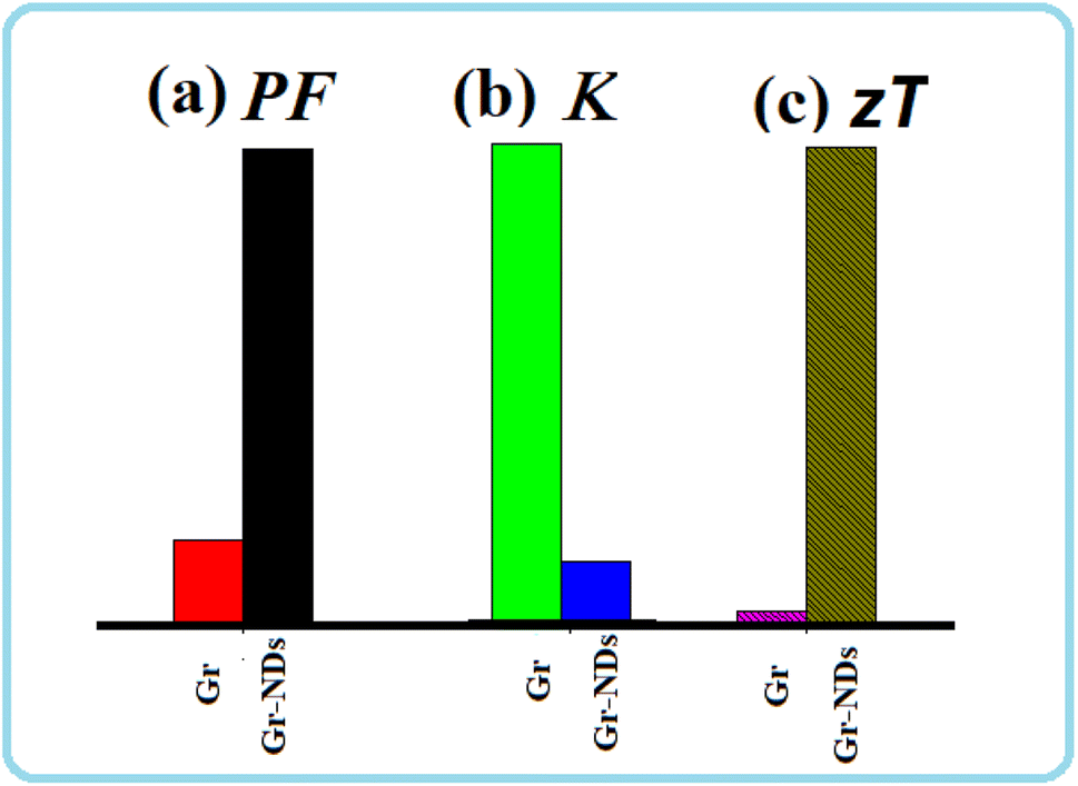 | ||
| Fig. 5 Normalized (a) power factor, PF, (b) thermal conductivity, κ (c) and figure of merit, zT of the Gr–NDs nanocomposite and their comparison with the values of pure graphene at RT. | ||
The reasons behind the increase in the electrical conductivity of the fabricated nanocomposite might be related to the modifications induced in the charge carrier density and electron mobility.29 Additionally, diamond nanoparticles of tiny sizes (between 3 and 8 nm) create bridges between exfoliated graphene layers and increase the number of phonon transport pathways in the through-direction, which can enhance the ratio of in-plane to through-plane thermal conductivity.23,30 Therefore, the Gr–NDs nanocomposite exhibits anisotropic thermal characteristics with high in-plane thermal conductivity due to its inherent 2D structure. In Fig. 6, we demonstrated an illustration to summarize and describe the possible mechanism of enhancing the TE properties of the produced Gr–NDs nanocomposites. This enhancement in the TE performance is most probably achieved due to (i) the formation of more charged defects, particularly at the edge of the formed sliced sheets, which can increase the density of charge carriers, then the electrical conductivity, (ii) filtering the high energy charge carriers, due the presence of more boundaries and interfacing sites, which can lead to an increase in the Seebeck coefficient, and (iii) increasing the scattered photons, which also due to the presence of more boundaries, humps/rough surfaces and more interfacing sites, which can scatter more phonons, then reduce the thermal conductivity.
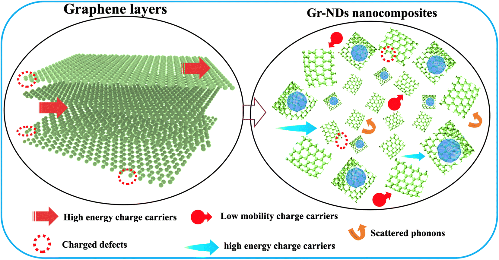 | ||
| Fig. 6 An illustration describing the possible mechanism of enhancing the TE properties of the Gr–NDs nanocomposites, which is due to (i) the formation of more charged defects, then increasing the density of charge carriers, (ii) filtering the high energy charge carriers, then increasing the Seebeck coefficient, and (iii) increasing the scattered phonons, which reduce the thermal conductivity. | ||
Power measurements
Fig. 7a and b show the above and near RT thermoelectric power characteristics of a single-leg rectangle-shaped TE module made of the Gr–NDs nanocomposite in compact pellet form. This small leg has a dimension of 2 × 6 × 10 mm (Fig. 7c). The output power was generated at different ΔT values (i.e., 20, 40, and 60 K). Fig. 7a shows the output voltage vs. current at different values of ΔT generated by a single-leg module made of the Gr–NDs nanocomposite sample. The sample showed systematic enhancements in the voltage, current, and power output values with increasing the value of ΔT. The maximum power achieved at ΔT = 60 K was approximately 6 nW, with a current equal to 60 μA (Fig. 7b). As a TE generator for electronic devices, it is required to use many p–n pairs made of different TE materials. The present Gr–NDs nanocomposite can be considered as the p-type part, and another appropriate n-type TE material can form the desired TE generator that can raise the power output for practical applications. However, as mentioned above further development for the Gr–NDs nanocomposite as a TE material is still needed, perhaps by coating with conducting polymers. This will be reported in further work. | ||
| Fig. 7 Above and near RT thermoelectric power characteristics of a single leg TE module made of the Gr–NDs nanocomposite in compact rectangular form (of 2 × 6 × 10 mm) at different ΔT values. (a) Open and closed-circuit values of V vs. I, (b) power output vs. I, and (c) dimensions of the used single-leg using rectangle-shape module. | ||
Conclusions
This study aimed to explore the TE properties of the produced 2D ultrafine Gr–NDs nanocomposite. It is observed that reducing the size of the graphene sheets using this approach e.g., by adding a small percentage of NDs in an organic solvent is found to be effective to enhance both the electrical conductivity and Seebeck coefficient and hence the power factor. This 2D nanocomposite structure also has much smaller thermal conductivity than that of the original graphene, which is useful for higher figures of merit. However, for practical applications, further enhancement is needed, which might be done by coating with some conducting polymers like polypyrrole, polyaniline, or PEDOT·PSS to further enhance the TE properties of this newly developed nanocomposite material.Author contributions
Ibrahim K. Alsulami: material synthesis, characterization, data curation, writing – original draft. Shittu Abdullahi: thermal conductivity, power measurement, data analysis, revising & editing. Ahmed Alshahrie: data analysis, investigation. Numan Salah: conceptualization, TE measurements, supervision, revising & editing.Conflicts of interest
The authors declare that they have no conflict of interest.Acknowledgements
The authors gratefully acknowledge the financial support provided by KACARE-KAU Research Fellowship Program for the Post-graduate students.Notes and references
- M. S. Dresselhaus, G. Chen, M. Y. Tang, R. Yang, H. Lee, D. Wang, Z. Ren, J. P. Fleurial and P. Gogna, Adv. Mater., 2007, 19, 1043–1053 CrossRef CAS.
- J. W. Jiang, J. S. Wang and B. Li, Phys. Rev. B: Condens. Matter Mater. Phys., 2009, 79, 205418 CrossRef.
- M. Uzair Khan, A. Naveed, S. Ehtisham Gillani, D. Awan, M. Arif, S. Afridi, M. Hamyun, M. Asif, S. Tabassum, M. Sadiq, M. Lais, M. Aslam, S. Ullah Jan and Z. Ahad, Mater. Res. Express, 2021, 8, 056302 CrossRef.
- D. Akinwande, C. J. Brennan, J. S. Bunch, P. Egberts, J. R. Felts, H. Gao, R. Huang, J. S. Kim, T. Li, Y. Li, K. M. Liechti, N. Lu, H. S. Park, E. J. Reed, P. Wang, B. I. Yakobson, T. Zhang, Y. W. Zhang, Y. Zhou and Y. Zhu, Extreme Mech. Lett., 2017, 13, 42–77 CrossRef.
- Y. Lin, M. Wood, K. Imasato, J. J. Kuo, D. Lam, A. N. Mortazavi, T. J. Slade, S. A. Hodge, K. Xi, M. G. Kanatzidis, D. R. Clarke, M. C. Hersam and G. J. Snyder, Energy Environ. Sci., 2020, 13, 4114–4121 RSC.
- Y. Liu, X. Duan, Y. Huang and X. Duan, Chem. Soc. Rev., 2018, 47, 6388–6409 RSC.
- J. Wang, X. Mu and M. Sun, Nanomaterials, 2019, 9, 218 CrossRef CAS PubMed.
- A. Bulusu and D. G. Walker, Superlattices Microstruct., 2008, 44, 1–36 CrossRef CAS.
- X. Chen, K. Shehzad, L. Gao, M. Long, H. Guo, S. Qin, X. Wang, F. Wang, Y. Shi, W. Hu, Y. Xu and X. Wang, Adv. Mater., 2020, 32, 1902039 CAS.
- Q. Zhang, T. Fang, F. Liu, A. Li, Y. Wu, T. Zhu and X. Zhao, Chem.–Asian J., 2020, 15, 2775–2792 CrossRef CAS PubMed.
- A. M. Ibrahim and D. A. Thompson, Mater. Chem. Phys., 1985, 12, 29–36 CrossRef CAS.
- T. Inohara, Y. Okamoto, Y. Yamakawa, A. Yamakage and K. Takenaka, Appl. Phys. Lett., 2017, 110, 183901 CrossRef.
- K. Synoradzki, K. Ciesielski, L. Kępiński and D. Kaczorowski, Phys. B, 2018, 536, 659–663 CrossRef CAS.
- J. Bitenieks, K. Buks, R. Merijs-Meri, J. Andzane, T. Ivanova, L. Bugovecka, V. Voikiva, J. Zicans and D. Erts, Polymers, 2021, 13, 4264 CrossRef CAS PubMed.
- G. J. Snyder and E. S. Toberer, Nat. Mater., 2008, 7, 105–114 CrossRef CAS PubMed.
- J. R. Sootsman, D. Y. Chung and M. G. Kanatzidis, Angew. Chem., Int. Ed., 2009, 48, 8616–8639 CrossRef CAS PubMed.
- S. Deng, X. Cai, Y. Zhang and L. Li, Carbon, 2019, 145, 622–628 CrossRef CAS.
- L. Venema, J. Janssen, M. Buitelaar, J. Wildöer, S. Lemay, L. Kouwenhoven and C. Dekker, Phys. Rev. B: Condens. Matter Mater. Phys., 2000, 62, 5238 CrossRef CAS.
- U. Mehmood, H. Asghar, F. Babar and M. Younas, Sol. Energy, 2020, 196, 132–136 CrossRef CAS.
- I. K. Alsulami, A. Saeed, S. Abdullahi, A. H. Hammad, A. Alshahrie and N. Salah, Diamond Relat. Mater., 2022, 130, 109411 CrossRef CAS.
- I. K. Alsulam, T. M. D. Alharbi, M. Moussa and C. L. Raston, ACS Omega, 2019, 4, 19279–19286 CrossRef CAS PubMed.
- A. Bisht, S. S. Samant, S. Jaiswal, K. Dasgupta and D. Lahiri, Composites, Part A, 2020, 132, 105840 CrossRef CAS.
- I. K. Alsulami, A. Saeed, S. Abdullahi, A. Alshahrie and N. Salah, FlatChem, 2022, 36, 100432 CrossRef CAS.
- M. Engenhorst, J. Fecher, C. Notthoff, G. Schierning, R. Schmechel and S. M. Rosiwal, Carbon, 2015, 81, 650–662 CrossRef CAS.
- C. Haslam, S. Damiati, T. Whitley, P. Davey, E. Ifeachor and S. A. Awan, Diagnostics, 2018, 8, 5 CrossRef PubMed.
- X. Huang, T. Leng, T. Georgiou, J. Abraham, R. Raveendran Nair, K. S. Novoselov and Z. Hu, Sci. Rep., 2018, 8, 1–7 CrossRef.
- N. A. Bogachev, A. A. Betina, T. S. Bulatova, V. G. Nosov, S. S. Kolesnik, I. I. Tumkin, M. N. Ryazantsev, M. Y. Skripkin and A. S. Mereshchenko, Nanomaterials, 2022, 12, 2972 CrossRef CAS PubMed.
- D. A. Rees and E. J. Welsh, Angew Chem. Int. Ed. Engl., 1977, 16, 214–224 CrossRef.
- M. Ohtaki, T. Tsubota and K. Eguchi, in International Conference on Thermoelectrics, ICT98, IEEE, 1998, pp. 610–613 Search PubMed.
- H. C. Yuan, C. Y. Lee and N. H. Tai, Compos. Sci. Technol., 2018, 167, 313–322 CrossRef CAS.
- P. Németh, K. McColl, R. L. Smith, M. Murri, L. A. J. Garvie, M. Alvaro, B. Pécz, A. P. Jones, F. Corà, C. G. Salzmann and P. F. McMillan, Nano Lett., 2020, 20, 3611–3619 CrossRef PubMed.
- A. J. Minnich, M. S. Dresselhaus, Z. F. Ren and G. Chen, Energy Environ. Sci., 2009, 2, 466–479 RSC.
- Y. Kinemuchi, C. Ito, H. Kaga, T. Aoki and K. Watari, J. Mater. Res., 2007, 22, 1942–1946 CrossRef CAS.
- A. A. Balandin, S. Ghosh, W. Bao, I. Calizo, D. Teweldebrhan, F. Miao and C. N. Lau, Nano Lett., 2008, 8, 902–907 CrossRef CAS PubMed.
- S. Ghosh, I. Calizo, D. Teweldebrhan, E. P. Pokatilov, D. L. Nika, A. A. Balandin, W. Bao, F. Miao and C. N. Lau, Appl. Phys. Lett., 2008, 92, 151911 CrossRef.
- W. Cai, A. L. Moore, Y. Zhu, X. Li, S. Chen, L. Shi and R. S. Ruoff, Nano Lett., 2010, 10, 1645–1651 CrossRef CAS PubMed.
- J. S. Heron, T. Fournier, N. Mingo and O. Bourgeois, Nano Lett., 2009, 9, 1861–1865 CrossRef CAS PubMed.
- G. J. Snyder, M. Christensen, E. Nishibori, T. Caillat and B. B. Iversen, Nat. Mater., 2004, 3, 458–463 CrossRef CAS PubMed.
Footnote |
| † Electronic supplementary information (ESI) available. See DOI: https://doi.org/10.1039/d3ra03748g |
| This journal is © The Royal Society of Chemistry 2023 |