
 Open Access Article
 This Open Access Article is licensed under a Creative Commons Attribution-Non Commercial 3.0 Unported Licence
Investigation of conduction mechanism and UV light response of vertically grown ZnO nanorods on an interdigitated electrode substrate
Khizar Hayat *a,
Zubair Alia,
Vineet Tirthbc,
Ali Algahtanibc,
Tawfiq Al-Mughanamd,
Abdulaziz H. Alghtanie,
Hussein Alrobeif,
Abdullah Shahg,
Ejaz Ahmeda and
Said Karim Shah*a
*a,
Zubair Alia,
Vineet Tirthbc,
Ali Algahtanibc,
Tawfiq Al-Mughanamd,
Abdulaziz H. Alghtanie,
Hussein Alrobeif,
Abdullah Shahg,
Ejaz Ahmeda and
Said Karim Shah*a
aDepartment of Physics, Abdul Wali Khan University Mardan, 23200-Mardan, Khyber Pakhtunkhwa, Pakistan. E-mail: khizar3@awkum.edu.pk; saidkarim@awkum.edu.pk
bMechanical Engineering Department, College of Engineering, King Khalid University, Abha 61421, Asir, Kingdom of Saudi Arabia
cResearch Center for Advanced Materials Science (RCAMS), King Khalid University, Guraiger, P.O. Box 9004, Abha-61413, Asir, Kingdom of Saudi Arabia
dDepartment of Mechanical Engineering, College of Engineering, King Faisal University, P. O. Box 380, Al-Ahsa 31982, Kingdom of Saudi Arabia
eDepartment of Mechanical Engineering, College of Engineering, Taif University, P.O. Box 11099, Taif 21944, Kingdom of Saudi Arabia
fDepartment of Mechanical Engineering, College of Engineering, Prince Sattam bin Abdul Aziz University, Al-Kharj, 11942, Saudi Arabia
gDepartment of Mathematics, College of Computing and Mathematics, King Fahd University of Petroleum and Minerals, Dhahran 31261, Saudi Arabia
First published on 5th July 2023
Abstract
Vertically aligned zinc oxide nanorod (ZnO-NR) growth was achieved through a wet chemical route over a comb-shaped working area of an interdigitated Ag–Pd alloy signal electrode. Field-emission scanning electron microscopy images confirmed the formation of homogeneous ZnO-NRs grown uniformly over the working area. X-ray diffraction revealed single-phase formation of ZnO-NRs, further confirmed by energy-dispersive X-ray spectroscopy analysis. Temperature-dependent impedance and modulus formalisms showed semiconductor-type behavior of ZnO-NRs. Two electro-active regions i.e., grain and grain boundary, were investigated which have activation energy ∼0.11 eV and ∼0.17 eV, respectively. The conduction mechanism was investigated in both regions using temperature-dependent AC conductivity analysis. In the low-frequency dispersion region, the dominant conduction is due to small polarons, which is attributed to the grain boundary response. At the same time, the correlated barrier hopping mechanism is a possible conduction mechanism in the high dispersion region attributed to the bulk/grain response. Moreover, substantial photoconductivity under UV light illumination was achieved which can be attributed to the high surface-to-volume ratio of zinc oxide nanorods as they provide high density of trap states which causes an increase in the carrier injection and movement leading to persistent photoconductivity. This photoconductivity was also facilitated by the frequency sweep applied to the sample which suggests the investigated ZnO nanorods based IDE devices can be useful for the application of efficient UV detectors. Experimental values of field lowering coefficient (βexp) matched well with the theoretical value of βS which suggests that the possible operating conduction mechanism in ZnO nanorods is Schottky type. I–V characteristics showed that the significantly high photoconductivity of ZnO-NRs as a result of UV light illumination is owing to the increase in number of free charge carriers as a result of generation of electron–hole pairs by absorption of UV light photons.
1. Introduction
Optoelectronics is one of the essential technological fields which focused on the electrical devices to recognize and regulate light sources. Light sensitive and photon generating devices are the two categories of optoelectronics that directly convert photons into electrical signals and vice versa.1 Photodetectors or photosensors materials absorb photons and produce electron–hole pairs.2 Absorb photons can be in the range of X-rays, ultraviolet (UV), infrared, and visible light depending upon the characteristics of the materials thus can find application in various fields including photonics, biomedical applications, security, environmental sensing, safety detectors, photo-sensing and object-tracking, etc.3 Similarly, low noise level and high photosensitive UV light detectors are needed as some pollution detection relies on measuring the strength of absorption lines for ozone, nitrous oxide, and sulphur dioxide as CdS and Si-based light detectors has some limitations in UV photodetection.4,5 Furthermore, better structural compatibility, chemical stability and device miniaturization with high response speed of photodetectors is the key focus of researchers which can be achieved via nanostructures of materials that have high surface to volume ratio.6–9 In this regard, zinc oxide nanostructure based photodetectors have received more attention due to their high light sensitivity in the UV range.10 Zinc oxide is a wide-direct-band gap semiconductor with room temperature bandgap energy of ∼3.37 eV and its high exciton binding energy is around 60 meV.11–13 It has quite high thermal stability, is a low cost material, non-toxic and transparent, has higher optical gain, a specific crystalline orientation, electrical conductivity,14,15 and is rich in various morphologies.16 ZnO is a promising material for use in a variety of photoelectric elements, including solar cells, and light-emitting devices.17 Furthermore, ZnO has the favorite wurtzite structure (along c-axis the polar surfaces terminate in Zn2+ and O2−) allowing it to create different 1D and 2D nanostructures.18 ZnO nanorods (ZnO-NRs), on the other hand, are more desirable because of their improved carrier confinement and high density of surface trap energy states, which can improve the electrical characteristics and performance of UV photodetectors.19,20 Investigation of various electro-active region and their qualitative as well as quantitative response to the signal is also very important which can further improve the performance of photodetectors. Likewise, for practical implementation, high temperature stable electrodes, cost effective and suitable substrate selection for photodetector devices is quite important whose performance does not affect within operating temperature variation. Various techniques are used to synthesized ZnO-NRs including hydrothermal,21 coprecipitation,22 solvothermal,23 wet chemical route,24 chemical & physical vapor deposition,25,26 etc. Among these techniques, bottom-up wet chemical route has more advantages such as it is mass production technique, easy to obtain uniform ZnO nanorods growth on substrates particularly, controlled growth can be achieved at temperature of less than 100 °C, almost no use of surfactants, etc.In nanotechnology, it is always a keen interest of the researchers to develop new sophisticated, easy and cost effective synthesis techniques or modify the existing techniques to obtain the desired materials at optimum conditions for particular applications. Secondly, qualitative as well as quantitative knowledge is necessary regarding various electro-active regions in the investigating materials which is always reflected as overall measurable response of the material particularly in the electrical properties. In this manuscript we present a bottom-up wet chemical route for the growth of ZnO nanorods on comb-shaped working area of Ag–Pd signal electrode already deposited on alumina substrate by photolithography technique. This photodetector is named as ZnO-NRs based IDEs device or metal–semiconductor–metal (MSM) photosensor that may have the advantage over other photodetectors to work in a wide operating temperature range. Another key novelty of this work is to investigate various electro-active regions qualitatively as well as quantitatively using temperature dependent impedance and modulus spectroscopy. Possible operating AC conduction mechanism was investigated by measuring the AC conductivity of ZnO-NR's based IDE device at different temperatures and frequency varying from 10 Hz to 5 MHz. UV light response of the device was carried out using AC conductivity and impedance formalism. Temperature dependent current vs. voltage characteristics of ZnO-NRs were measured to investigate possible DC conduction mechanism. UV light photo-response of ZnO-NRs was also measured at room temperature.
2. Experimental section
2.1. Materials
Ammonium hydroxide (NH3OH, 32%, Merck, analytical grade), zinc-nitrate hexahydrate (Zn(NO3)2·6H2O, Sigma, purity ≥ 99.0%), deionized water (DIW), interdigitated Ag–Pd signal electrodes (IDEs), acetone (extra pure) and ethanol (analytical grade) were used as precursors for the synthesis of ZnO nanorods vertical growth on working area of substrate. These chemicals were used directly without further purification. Signal electrodes were purchased from Elite Tech. Ltd., Beijing, China. The details of each signal electrode is summarized as follows.• Length = 6 mm
• Width = 3 mm
• No. of combs in each electrode = 5
• Distance between any two consecutive combs = 0.2 mm
• Electrode material = Ag![[thin space (1/6-em)]](https://www.rsc.org/images/entities/char_2009.gif) :Pd (70:30) alloy
:Pd (70:30) alloy
• Substrate = alumina (Al2O5)
2.2. Synthesis procedure
Interdigitated electrodes (IDEs, also called Ag–Pd signal electrodes) were first clean subsequently with distilled water, acetone and ethanol in ultrasonic bath for few minutes at ambient temperature and then dried in oven at 120 °C/30 min. Zn(NO3)2·6H2O of 2.975 g was added to 100 ml DIW and stirred for 30 min to get 0.1 M solution. Then, 3.5 ml ammonium hydroxide solution was added drop by drop to zinc nitrate solution and combined solution was further stirred for about 30 min. A clean Teflon made electrode holder was placed inside this final solution holding IDE horizontally at position around 1 cm down from the surface of solution upper level as shown in Fig. 1. The signal electrode side of IDE substrate was kept downward. The glass beaker was covered by aluminum foil and then heat treated it in oven at 90 °C for 6 h. After reaction completion, IDE substrate was genteelly washed with deionized water to clean ZnO nanorod's surfaces and to remove any unwanted residuals. Growth substrate was finally dried in oven at 60 °C for 2 hours.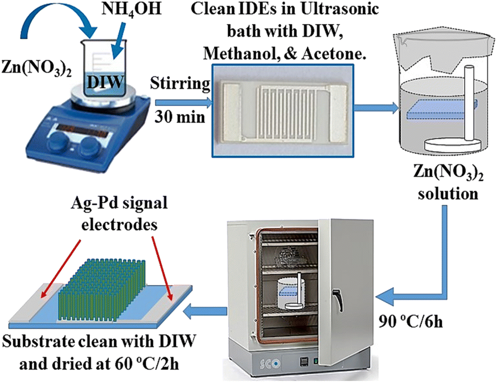 | ||
| Fig. 1 Schematic diagram showing the synthesis procedure of vertically grown ZnO-NRs on the working area of IDE substrate using wet chemical route. | ||
2.3. Characterizations
Field-emission scanning-electron-microscope (FE-SEM, made by TESCAN MAIA3, UK) was used to study the morphology and uniformity of vertically grown ZnO-NRs on IDE substrate. Elemental composition was carried out using Octane Elite Detector equipped with FESEM. X-ray diffractometer (XRD, Philips) with CuKα1 radiation source (λ = 1.5406 Å) was used to examine the structure and phase purity of ZnO NRs. The angle 2θ was varied from 20 to 80°. Precision impedance analyzer (MICROTEST, 6630, Taiwan) connected with furnace was used to measure the impedance and AC conductivity of ZnO-NRs based IDE device at different temperatures. A small AC voltage of 100 mV was applied to sample. For photo response of device, a handheld UV lamp analyzer (Model: ZF-5, China) having wavelengths 254 nm and 365 nm was used. Temperature dependent I–V characteristics and UV light response of ZnO-NRs were measured using 2401 Keithley SourceMeter Unit (SMU).3. Results and discussion
3.1. Structural analysis
Fig. 2 shows the X-ray diffraction (XRD) pattern of ZnO nanorod's powder obtained from growth solution. The red lines show the standard XRD data of ZnO powder. All crystalline peaks were indexed with JCPDS card number 00-005-0664. Since, there is no extra peak in the XRD pattern and matched well with the standard, this indicates the formation of single phase polycrystalline ZnO nanorods.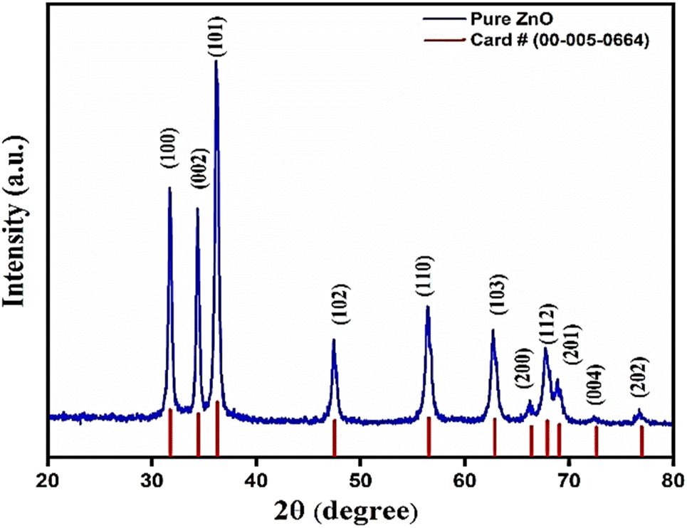 | ||
| Fig. 2 Zinc oxide nanorod's XRD powder pattern obtained from growth solution. | ||
3.2. Morphological analysis
Fig. 3(a) shows the FE-SEM image of vertically grown ZnO nanorods on combs-shaped working area of IDEs device via wet chemical route. A schematic diagram of Ag–Pd signal electrode is shown in the right top of Fig. 3(a). It is obvious from the figure that ZnO nanorods are grown uniformly/homogenously over the entire working are of the electrode. Fig. 3(b) shows the low and high (inset image) magnification FESEM image of ZnO-NRs on IDE substrate. This shows that ZnO nanorods are well aligned and grown vertically on the substrate. Fig. 3(c) shows the energy dispersive X-ray spectrum of ZnO-NRs. In this spectrum, the inset table shows the weight and atomic percentages of the elements in sample while the red spot on the FESEM image shows the scan area from where the elemental analysis was carried out. Since, no extra peak is found in EDS spectrum this indicates the formation of ZnO which support the XRD result as shown in previous Fig. 2.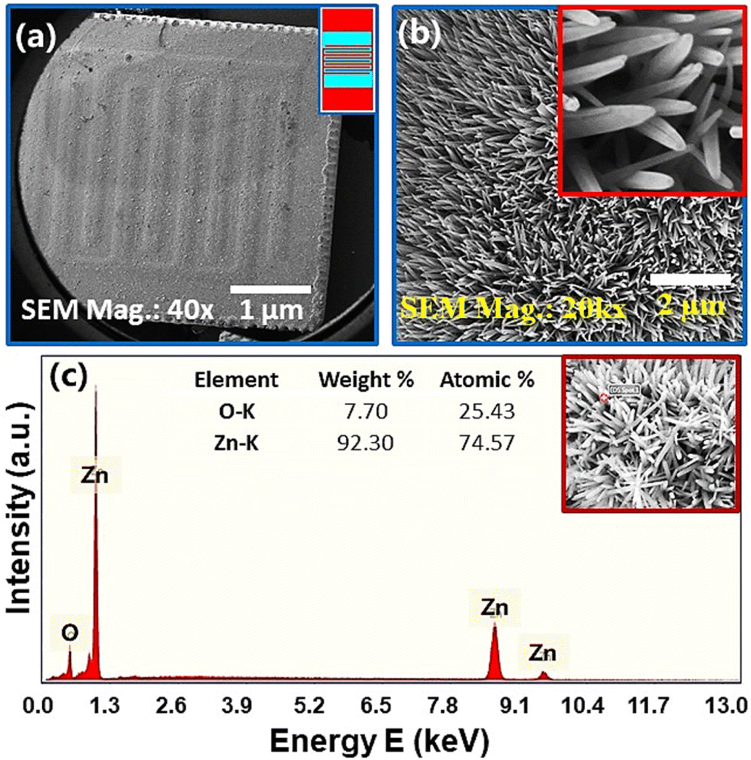 | ||
| Fig. 3 (a) FE-SEM images of vertically grown ZnO nanorods on combs-shaped working area of IDEs device via wet chemical route. (b) Low & high (inset image) magnification FE-SEM image of ZnO-NRs on IDE substrate. (c) Energy dispersive X-ray spectrum of ZnO-NRs. | ||
3.3. Impedance and modulus spectroscopy
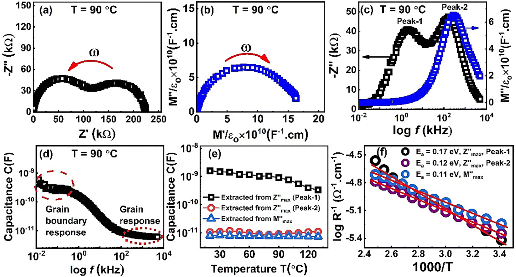
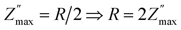
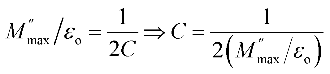
Nyquist plots of impedance formalism of ZnO-NRs based IDE device measured in a frequency sweep from 10 Hz to 5 MHz as shown in Fig. 4. Temperature of device was varied from 20 to 130 °C with a step of 10 °C. There are two semicircular arcs at each Nyquist plot which indicates two different electro-active regions in the sample. Increasing the temperature, the diameter of semicircular arcs decreased which indicates semiconductor nature of the sample. In order to quantitatively describe these two different electroactive regions, the data was replotted in impedance and modulus formalisms at a single temperature i.e., 90 °C as shown in Fig. 5.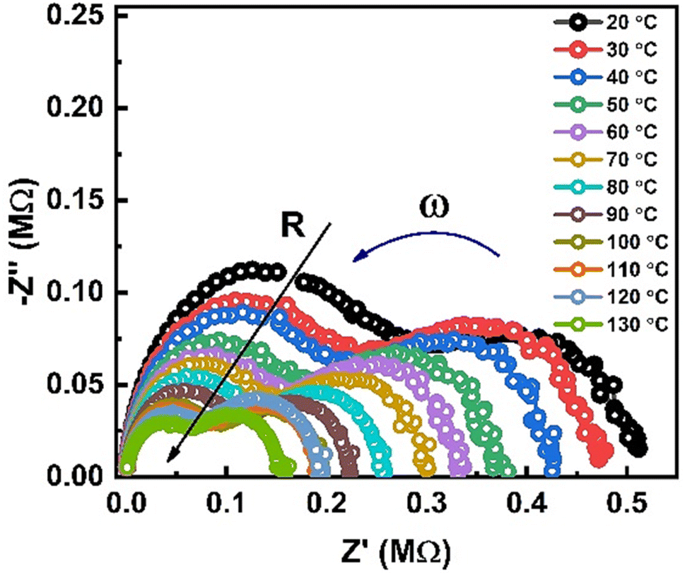 | ||
| Fig. 4 Nyquist plot of ZnO rod's based IDEs device recorded at different temperatures. | ||
 | ||
| Fig. 5 Graph of impedance spectroscopy results recorded at 90 °C. | ||
Fig. 5(a) and (b) shows the Nyquist plots of impedance and modulus formalism at a temperature 90 °C. Impedance formalism highlights the resistive region of the sample while modulus formalism reflects the conductive electro-active region in the sample. In both formalisms the direction for frequency variation is shown by a curved arrow. The impedance Nyquist plot indicated two different electro-active regions while the modulus shows a single conductive region in the sample. For more in depth understanding the real components of impedance and modulus were plotted against frequency as shown in Fig. 5(c). There are two Debye peaks in impedance spectroscopic plot while one Debye peak is found in modulus spectroscopic plot. In impedance spectroscopic plot the Debye peak maxima is proportional to resistance “R” while in modulus spectroscopic plot the Debye peak maxima 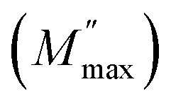 is inversely related to the capacitance “C” as given in eqn (1) and (2).27,28
 | (1) |
 | (2) |
If any of these two parameters (R or C) is given, then one can easily calculate the other parameter using the following eqn (3).
| ωmax = RC | (3) |
Capacitance vs. frequency plot is shown in Fig. 5(d). In low frequency region the capacitance value is high and its value is in “nanofarad” which represents a resistive region and is named as the grain boundary response. While in high frequency region the capacitance value is small and in “picofarad” which indicates the grain response of the sample. In order to further explore these electro-active regions, the capacitance values extracted from Debye peak maxima in both impedance and modulus formalisms and are plotted against temperature as shown in Fig. 5(e). It is obvious from this graph that in impedance spectroscopic plot the associated capacitance with peak-1 at lower frequency is high which corresponds to a resistive region in the sample and hence attributed to the grain boundary region. However, the capacitance values associated with peak-2 and that in the modulus formalism corresponds to same conductive region or grain based on low capacitance values. Debye peak maxima in both formalisms were used to calculate the conductivity of these electro-active regions. Fig. 5(f) shows Arrhenius conductivity plot extracted from Debye peak maxima. A straight line was fit in the data and the value of slope “s” was used to calculate the activation energy. Obtained activation energy values for bulk/grain and grain boundary regions are 0.11 eV and 0.17 eV, respectively.
3.4. AC conductivity analysis
Total AC conductivity of materials can be expressed mathematically as follows.29| σtotal = σdc + σac | (4) |
Fig. 6 shows the plot of total AC conductivity of ZnO-NR's based IDE device recorded at various temperatures. At each temperature, in the low frequency region, the conductivity is almost frequency independent which increased with increasing the temperature. This indicates dc type conduction mechanism which is thermally activated and it is attributed to the drift of accumulated charge carriers at the boundary region. By further increasing the frequency, at each temperature two dispersion regions were observed indicating frequency dependent conductivity (σac = Aωs) in the sample as shown in Fig. 6(a). The value of exponent “s” was evaluated as follows.
| σac = Aωs ⇒ ln(σac) = ln(Aωs) = ln(A) + s × ln(ω) |
| As, ln(x) = 2.303log(x) |
| 2.303log(σac) = 2.303logA + 2.303slog(ω) |
|
log(σac) = 2.303log(A) + s × log(ω)
| (5) |
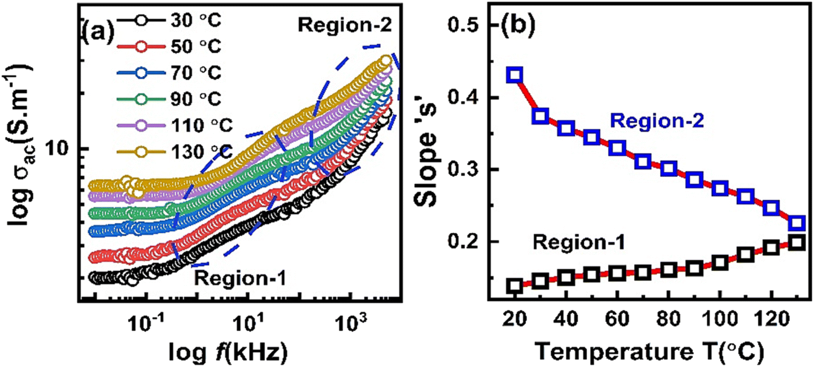 | ||
| Fig. 6 AC conductivity of ZnO nanorod's based IDEs device recorded at different temperature. | ||
Eqn (5) represents a straight line equation between log(σac) vs. log(ω), where “2.303log(A)” denotes the y-intercept of straight line and ω = 2πf.
According to eqn (5), in both region-1 and region-2, an equation of straight line was fitted in the data points and slope “s” value was noted in both regions at all temperatures. Fig. 6(b) shows the plot of parameter “s” with temperature for both regions. It is obvious that in region-1, parameter “s” slightly increases with increasing the temperature which suggests Small Polaron (SP) conduction in the sample at grain boundary region. However, in region-2, parameter “s” decreases with increasing temperature. This suggests correlated barrier hopping (CBH) type mechanism in sample that operate in the bulk or grain region of the sample.32,33
3.5. UV light response via IS and AC conductivity
Fig. 7 shows the UV light response of ZnO nanorod's based IDEs device. Data is measured in dark, ambient light, UV light of wavelength 254 nm, 365 nm and combined 354 & 365 nm. Fig. 7(a) shows the Nyquist plots with and without light illumination. In dark, the sample resistance is quit high and under ambient light the resistance decreased. However, there is a significant decrease in resistance under the UV light illumination of wavelength 254 nm which further decreased under 365 nm and combined 254 & 365 nm wavelengths as shown in the inset in Fig. 7(a). AC conductivity plots in Fig. 7(b) also indicates a significant increase in conductivity of ZnO-NRs based IDE device under the illumination of UV light photons. Overall impedance of device was also measured under the same condition which also shows a significant decreased in total impedance of the sample under UV light illumination as shown in Fig. 7(c). The substantial photoconductivity under UV light illumination can be attributed to the high surface-to-volume ratio of zinc oxide nanorods. As, the free surfaces are the origin of trap energy states and high density of these trap states causes an increase of carrier's injection and transport which leads to a persistent photoconductivity.34,35 Furthermore, another factor including in the significant promotion of carrier's transport through investigating ZnO-NRs based IDE device is the applied frequency sweep which facilitates the carrier's flow. This suggests that the investigating ZnO-NRs based IDE device can be useful for the application of UV detection.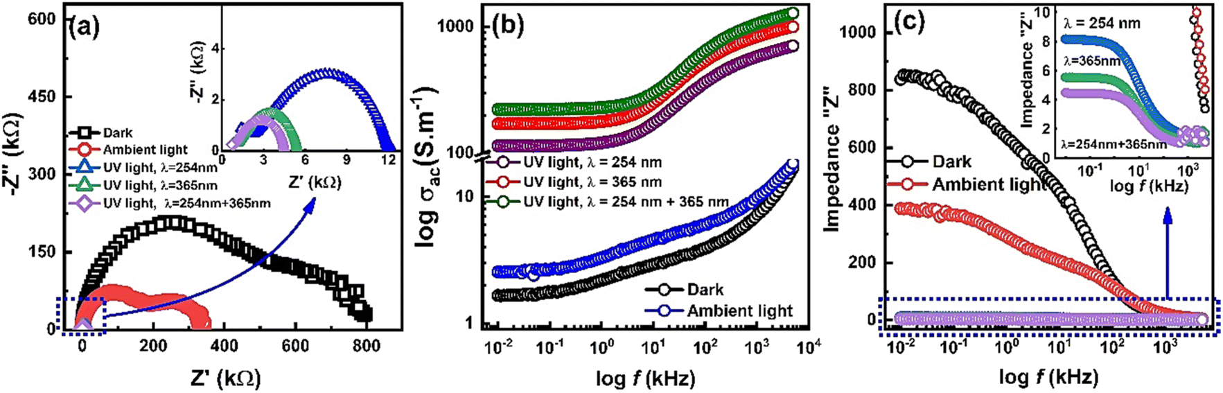 | ||
| Fig. 7 Light response of ZnO-NRs based IDEs device recorded at room temperature via impedance spectroscopy and AC conductivity. | ||
3.6. Current–voltage characteristics
DC conduction mechanisms are generally classified into following two categories.• Electrode or injection limited conduction mechanisms that operate at electrode–sample interface or contact. Some of these mechanisms include Schottky-emission, Fowler Nordheim tunneling, direct tunneling, thermionic field emission, etc.
• Bulk or transport limited conduction mechanisms that exists inside the material under investigation. These mechanisms are Poole–Frenkel mechanism, ohmic conduction, hopping conduction, space charge limited conduction, grain boundary limited conduction, etc.
Since various conduction mechanisms contribute to the overall current response in the given applied field region followed by temperature variation; therefore, it is necessary to investigate and distinguish these conduction mechanisms.
Fig. 8(a) shows current vs. voltage characteristic curves of ZnO-NRs based IDEs device measured from −10 to +10 V at different temperatures. The I–V curves are non-linear and are influenced by the temperature. This indicates a semiconductor type behavior of ZnO nanorods as a result of change in the carrier's concentration, mobility and recombination rates. The temperature dependent I–V characteristics provide quite fruitful investigations regarding transport properties such as mobility, carrier's concentration, activation energy, operating conduction mechanism according to power law J ∝ Vn, where “n” is a power index which predicts the possible operating conduction mechanism. In order to investigate the conduction mechanism, the data was replotted on logarithmic scale in the form of ln(J) vs. ln(V) as shown at temperature 20 °C in Fig. 8(c). Each ln(J)–ln(V) curve shows two different regions. Low voltage region is named as “region-I” while that of high voltage is called “region-II”. A linear is fitted in both regions at all temperatures and the slopes value are plotted against temperature as shown in Fig. 8(c). At the lower voltages “region-I” the slopes of 0.988 ≤ n ≤ 1.035 show ohmic conduction while at the higher voltages the slopes of 1.356 ≤ n ≤ 1.274 indicate some non-ohmic conduction.
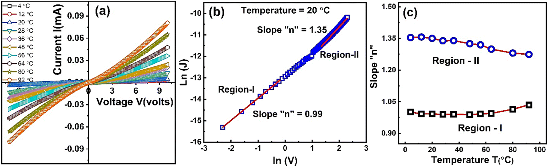 | ||
| Fig. 8 (a) Current versus voltage curves of ZnO-NRs based IDEs device recorded at different temperatures, (b) ln(J) vs. ln(V) curve at 20 °C, & (c) slope “n” variation with respect to temperature. | ||
Three worth mentioning conduction processes namely space-charge-limited current, Schottky and Poole–Frenkel mechanisms are responsible for high voltage non-ohmic region. At medium fields, charge injection from metal electrode to material sample (a semiconductor or an insulator) may take place by field-assisted-thermionic emission called Richardson–Schottky effect or simply Schottky emission. During this process an image force induced which tries to lower the potential energy barrier for the emission of charge carriers under the influence of applied electric field. Secondly, in bulk of the material, the carriers are produced by the dissociation of donor–acceptor centers due to field-enhanced thermal excitation of trapped electrons in to the conduction band which is termed as the Poole–Frenkel (PF) generation. Furthermore, if carrier's generation process is slower than carrier's transport via the bulk then the conduction is called either the Schottky or PF mechanism and if the carrier's transport is slower than carrier's generation then the conduction is termed as SCLC mechanism.36,37
The space-charge-limited current density (J) is given by the following eqn (6);
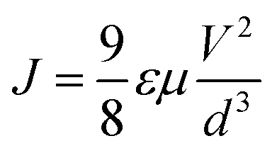 | (6) |
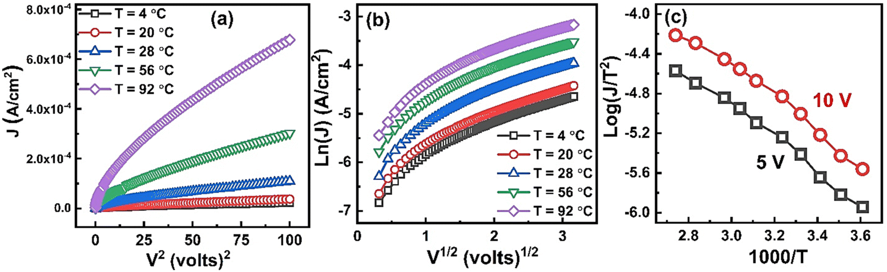 | ||
| Fig. 9 Plots of (a) J vs. V2, (b) log(J) vs. V1/2, & (c) log(J/T2) vs. 1000/T measured at different temperatures. | ||
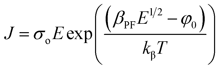
In the case of Schottky mechanism, the applied field at electrode–material interface interacts with the image force resulting in lowering the potential barrier. Due to this decrease in potential barrier, the electrode limited current does not saturate according to the Richardson law,39
 | (7) |
 | (8) |
 is the effective Richardson constant, kβ is the Boltzmann constant,
 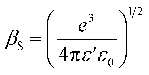 is the Schottky coefficient, E (=V/d) is the static electric field, and φo is the potential barrier without field.
Furthermore, the PF mechanism, which is a field assisted thermal ionization process, is the bulk analogue of the Schottky effect at an interfacial barrier. The corresponding expression for current density in PF mechanism is,
 | (9) |
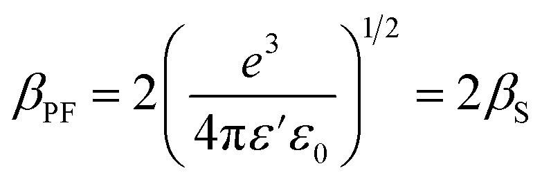
It is obvious from eqn (8) and (9) that the current density changes exponentially as the square root of the applied field. Both these equations suggest that ln(J) vs. E1/2 or ln(J) vs. V1/2 plot should be linear in nature for Schottky as well as PF type conduction mechanism. Therefore, it is suggested that a general expression for the current density can equally be valid for both PF and Schottky mechanisms of the following form,40,41
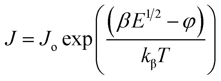 | (10) |
 | (11) |
Fig. 9(b) shows plot of ln(J) vs. V1/2 at different temperatures. It is clear that at all temperatures in the high field region the ln(J) is proportional to V1/2 which suggest that the possible operating conduction mechanism in ZnO nanorods may either be Schottky or PF type.
In order to differentiate these two mechanisms and to investigate the possible operating conduction mechanism, one must compare the experimental values of field lowering coefficient (βexp) with the theoretical values (i.e., βTh). βexp can be evaluated by taking the natural logarithm of both sides of eqn (10) as follows;
 | (12) |
| βexp = δkβTd1/2 | (13) |
 is the slope of linear fit. From the slope of straight line at high field region of ln(J) vs. V1/2 plots (as shown in Fig. 9(b)) at different temperatures, βexp can be evaluated using eqn (13). Also, high frequency dielectric constant value of ZnO nanorods (i.e., 2.02 at frequency > 1 MHz) was used to calculate theoretical values of βS & βPF using eqn (11). Values of βexp, βS & βPF are tabulated in Table 1. It is obvious from Table 1 that the values of βexp matched well with the theoretical value of βS. This suggests that the possible operating conduction mechanism in ZnO nanorods is Schottky type. Since, ln(J) vs. V1/2 graph shows a linear behavior, however, in Fig. 9(b) there is a nonlinear behavior at low voltage region. This divergence is most likely due to the accumulation of space charges near the electrodes, result in non-uniform field distribution between the electrodes.
| Temperature (°C) | β (eV m1/2 V−1/2) | ||
|---|---|---|---|
| βexp. | βS | βPF | |
| 4 | 2.30 × 10⁻⁵ | 2.67 × 10⁻⁵ | 5.34 × 10⁻⁵ |
| 12 | 2.42 × 10⁻⁵ | ||
| 20 | 2.54 × 10⁻⁵ | ||
| 28 | 2.48 × 10⁻⁵ | ||
| 36 | 2.52 × 10⁻⁵ | ||
| 48 | 2.61 × 10⁻⁵ | ||
| 56 | 2.69 × 10⁻⁵ | ||
| 64 | 2.69 × 10⁻⁵ | ||
| 80 | 2.77 × 10⁻⁵ | ||
| 92 | 2.85 × 10⁻⁵ | ||
Furthermore, in the plot of log(J/T2) vs. 1000/T at certain fixed voltage, the Richardson line shows a linear behavior with a negative slope. Fig. 9(c) shows plot of log(J/T2) vs. 1000/T at two different voltages 5 V & 10 V. The linear behavior with negative slope again confirm the existence of Schottky type conduction mechanism in ZnO nanorods sample.
3.7. UV light response via I–V curves
Fig. 10 shows current vs. voltage curves of ZnO-NRs based IDEs device recorded at room temperature under dark and illumination of visible and UV lights. Fig. 10(a) shows the I–V curves on the linear scale. Since, the I–V curve of the device measured in the dark is not visible clearly; therefore, the data is replotted on logarithmic scale as shown in Fig. 10(b). It is obvious that the I–V characteristics of ZnO-NRs are significantly affected by the illumination as well as intensity of UV light. This strong UV light absorption and emission properties of ZnO-NRs making them suitable candidates for finding potential applications specifically in optoelectronics and photonics. ZnO-NRs response to UV light can be explained in terms of their electronic and optical properties. When expose to UV light, ZnO-NRs exhibit a significant increase in the photoconductivity. Which is attributed to the increase in number of free charge carriers as a result of generation of electron–hole pairs by absorption of photons from UV light illumination. It is obvious from Fig. 10(b) that the photoconductivity also increased with increasing the wavelength of the UV light. Furthermore, other factors that contribute to the enhancement of photoconductivity of ZnO-NRs include the intensity of light, the presence of any surface defects, the doping level of ZnO-NRs (not in the present case), etc. However, in general, the significant UV light sensitive response of ZnO-NRs based IDE's device makes them promising materials for a wide range of applications such as optoelectronics, photonics, photocatalysis, sensors, solar cells, etc.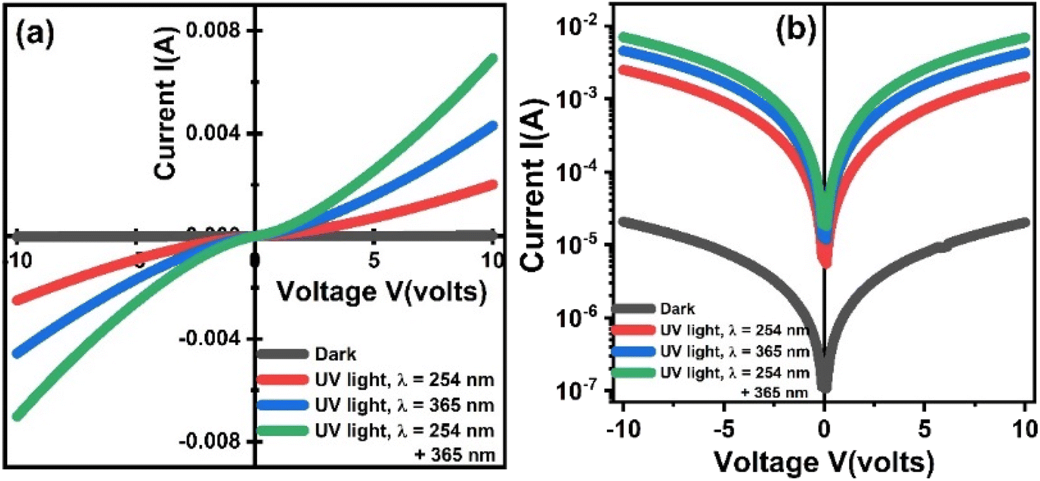 | ||
| Fig. 10 Room temperature light response of ZnO-NRs based IDEs device measured in the form of current–voltage characteristics. | ||
4. Conclusion
In this research work, zinc oxide nanorod's vertically growth conditions are optimized on over a comb-shaped working area of interdigitated Ag–Pd alloy signal electrode via wet chemical route. Morphology and uniformity of these nanorods were checked via FE-SEM. FE-SEM images confirmed uniform vertical growth of ZnO-NRs on IDE substrate. Crystal structure of sample was investigated via X-ray diffractometer which revealed the formation of single-phase polycrystalline zinc oxide with hexagonal structure. Energy dispersive X-ray spectrometer was used for elemental analysis to check sample purity and to support the XRD results. Impedance and modulus formalisms were used to investigate qualitatively as well as quantitatively various electro-active regions. Both formalisms have shown two different electro-active regions. These regions were names as grain and grain boundary based on the associated capacitance and conductivity values. Grain and grain boundary have activation energy ∼0.11 eV and ∼0.17 eV, respectively. AC conductivity analysis showed that in the low-frequency dispersion region, the dominant conduction is due to small polarons, which is attributed to the grain boundary response while correlated barrier hopping mechanism is the possible conduction mechanism in the high dispersion region and it is attributed to the grain. Furthermore, photosensitivity of the device was checked using UV light of two different wavelengths i.e., 254 nm & 365 nm. Substantial photoconductivity under UV light illumination was achieved which can be attributed to the high surface to volume ratio of ZnO-NRs as they provide high density of trap states which causes an increase of carrier's injection and transport that leads to a persistent photoconductivity. Furthermore, carrier's transport in ZnO-NRs based IDE device is also facilitated by frequency sweep applied to the sample which suggests that ZnO-NRs based IDE devices can be useful for the application of efficient UV detectors. Experimental values of β (i.e., βexp) matched well with the theoretical βS which indicates that Schottky type conduction mechanism is possible to operate in ZnO nanorods. Furthermore, the significantly high photoconductivity of ZnO-NRs in I–V curves as a result of UV light illumination is due to the increase in number of free charge carriers as a result of generation of electron–hole pairs by absorption of UV light photons.Author contributions
All authors contributed equally in the article in conceptualization, investigation, analysis, writing original draft, review and editing.Conflicts of interest
The authors declare no conflict of interest.Acknowledgements
The authors extend their appreciation to the Deanship of Scientific Research at King Khalid University Abha 61421, Asir, Kingdom of Saudi Arabia for funding this work through the Large Groups Project under grant number RGP.2/499/44. The authors acknowledge the Deanship of Scientific Research, Vice Presidency for Graduate Studies and Scientific Research at King Faisal University, Saudi Arabia, for financial support under the annual funding track [GRANT3753].References
- J. Haas, M. Schwartz, U. Rengstl, M. Jetter, P. Michler and B. Mizaikoff, Chem/bio sensing with non-classical light and integrated photonics, Analyst, 2018, 143, 593–605 RSC.
- Z. Zhao, J. Liu, Y. Liu and N. Zhu, High-speed photodetectors in optical communication system, J. Semicond., 2017, 38, 121001 CrossRef.
- S. Youssef, Y. M. El-Batawy and A. A. Abouelsaood, Effect of self assembled quantum dots on carrier mobility, with application to modeling the dark current in quantum dot infrared photodetectors, J. Appl. Phys., 2016, 120, 124506 CrossRef.
- F. González-Posada, R. Songmuang, M. Den Hertog and E. Monroy, Environmental sensitivity of nin and undoped single GaN nanowire photodetectors, Appl. Phys. Lett., 2013, 102, 213113 CrossRef.
- L. Sang, M. Liao and M. Sumiya, A comprehensive review of semiconductor ultraviolet photodetectors: from thin film to one-dimensional nanostructures, Sensors, 2013, 13, 10482–10518 CrossRef CAS PubMed.
- H. Chen, H. Liu, Z. Zhang, K. Hu and X. Fang, Nanostructured photodetectors: from ultraviolet to terahertz, Adv. Mater., 2016, 28, 403–433 CrossRef CAS PubMed.
- Y.-J. Hsiao, T.-H. Fang, L.-W. Ji and B.-Y. Yang, Red-shift effect and sensitive responsivity of MoS2/ZnO flexible photodetectors, Nanoscale Res. Lett., 2015, 10, 1–5 CrossRef CAS PubMed.
- T. Zhai, L. Li, Y. Ma, M. Liao, X. Wang, X. Fang, J. Yao, Y. Bando and D. Golberg, One-dimensional inorganic nanostructures: synthesis, field-emission and photodetection, Chem. Soc. Rev., 2011, 40, 2986–3004 RSC.
- S. N. Sarangi, B. C. Behera, N. K. Sahoo and S. K. Tripathy, Schottky junction devices by using bio-molecule DNA template-based one dimensional CdS-nanostructures, Biosens. Bioelectron., 2021, 190, 113402 CrossRef CAS PubMed.
- B. Cao, W. Cai, Y. Li, F. Sun and L. Zhang, Ultraviolet-light-emitting ZnO nanosheets prepared by a chemical bath deposition method, Nanotechnology, 2005, 16, 1734 CrossRef CAS.
- W. Li, G. He, J. Shao, Q. Liu, K. Xu, J. Hu and I. P. Parkin, Urchin-like MnO2 capped ZnO nanorods as high-rate and high-stability pseudocapacitor electrodes, Electrochim. Acta, 2015, 186, 1–6 CrossRef CAS.
- W. Zhang, Y. Sun, Z. Xiao, W. Li, B. Li, X. Huang, X. Liu and J. Hu, Heterostructures of CuS nanoparticle/ZnO nanorod arrays on carbon fibers with improved visible and solar light photocatalytic properties, J. Mater. Chem. A, 2015, 3, 7304–7313 RSC.
- J. Ge, Y. Sun, W. Chen, F. Song, Y. Xie, Y. Zheng and P. Rao, Z-scheme heterojunction based on NiWO4/WO3 microspheres with enhanced photocatalytic performance under visible light, Dalton Trans., 2021, 50, 13801–13814 RSC.
- S. Shen, J. Chen, L. Cai, F. Ren and L. Guo, A strategy of engineering impurity distribution in metal oxide nanostructures for photoelectrochemical water splitting, J. Materiomics, 2015, 1, 134–145 CrossRef.
- M. Zhu, N. Huang, J. Gong, B. Zhang, Z. Wang, C. Sun and X. Jiang, Growth of ZnO nanorod arrays by sol–gel method: transition from two-dimensional film to one-dimensional nanostructure, Appl. Phys., 2011, 103, 159–166 CAS.
- A. Bera and D. J. A. P. L. Basak, Role of defects in the anomalous photoconductivity in ZnO nanowires, Appl. Phys. Lett., 2009, 94, 163119 CrossRef.
- Ü. Özgür, Y. I. Alivov, C. Liu, A. Teke, M. Reshchikov, S. Doğan, V. Avrutin, S.-J. Cho and H. Morkoç, A comprehensive review of ZnO materials and devices, J. Appl. Phys., 2005, 98, 11 CrossRef.
- D. Agarwal, R. Chauhan, D. Avasthi, I. Sulania, D. Kabiraj, P. Thakur, K. Chae, A. Chawla, R. Chandra and R. Ogale, VLS-like growth and characterizations of dense ZnO nanorods grown by e-beam process, J. Appl. Phys., 2009, 42, 035310 Search PubMed.
- Y. Li, F. Della Valle, M. Simonnet, I. Yamada and J.-J. Delaunay, High-performance UV detector made of ultra-long ZnO bridging nanowires, Nanotechnology, 2008, 20, 045501 CrossRef PubMed.
- O. Lupan, L. Chow and G. Chai, A single ZnO tetrapod-based sensor, Sens. Actuators, B, 2009, 141, 511–517 CrossRef CAS.
- S. Worasawat, T. Masuzawa, Y. Hatanaka, Y. Neo, H. Mimura and W. Pecharapa, Synthesis and characterization of ZnO nanorods by hydrothermal method, Mater. Today: Proc., 2018, 5, 10964–10969 CAS.
- E. I. Naik, H. B. Naik, M. Sarvajith and E. Pradeepa, Co-precipitation synthesis of cobalt doped ZnO nanoparticles: Characterization and their applications for biosensing and antibacterial studies, Inorg. Chem. Commun., 2021, 130, 108678 CrossRef CAS.
- K. Wu, L. Zhou, C. Mao and Y. Chu, Solvothermal synthesis of ZnO with controllable morphology, Mater. Lett., 2023, 341, 134161 CrossRef CAS.
- H. Zhang, J. Feng, J. Wang and M. Zhang, Preparation of ZnO nanorods through wet chemical method, Mater. Lett., 2007, 61, 5202–5205 CrossRef CAS.
- O. Lupan, G. A. Emelchenko, V. V. Ursaki, G. Chai, A. Redkin, A. N. Gruzintsev, I. Tiginyanu, L. Chow, L. K. Ono and B. Cuenya, Synthesis and characterization of ZnO nanowires for nanosensor applications, Mater. Res. Bull., 2010, 45, 1026–1032 CrossRef CAS.
- G. Jimenez-Cadena, E. Comini, M. Ferroni, A. Vomiero and G. Sberveglieri, Synthesis of different ZnO nanostructures by modified PVD process and potential use for dye-sensitized solar cells, Mater. Chem. Phys., 2010, 124, 694–698 CrossRef CAS.
- K. Hayat, M. Rafiq, S. Durrani and M. M. Hasan, Impedance spectroscopy and investigation of conduction mechanism in BaMnO3 nanorods, Phys. B, 2011, 406, 309–314 CrossRef CAS.
- K. Hayat, M. Nadeem, M. Javid Iqbal, M. Rafiq and M. M. Hasan, Analysis of electro-active regions and conductivity of BaMnO3 ceramic by impedance spectroscopy, Appl. Phys. A, 2014, 115, 1281–1289 CrossRef CAS.
- K. Hayat, S. Ali, A. ur Rahman, S. Khan, S. Shah and Y. Iqbal, Effect of B-site dopants on the electrical properties of BaMn1−xAxO3 ceramics via low temperature impedance spectroscopy, Mater. Res. Express, 2018, 5, 086304 CrossRef.
- A. R. Long, Frequency-dependent loss in amorphous semiconductors, Adv. Phys., 1982, 31, 553–637 CrossRef CAS.
- E. V. Gopalan, K. Malini, S. Saravanan, D. S. Kumar, Y. Yoshida and M. R. Anantharaman, Evidence for polaron conduction in nanostructured manganese ferrite, Appl. Phys., 2008, 41, 185005 Search PubMed.
- F. Wahed, S. S. Shah, K. Hayat, S. K. Shah and M. A. Aziz, Conduction mechanisms and thermoelectric applications of La1−xSrxCoO3 nanofibers, J. Mater. Sci., 2022, 57, 8828–8844 CrossRef CAS.
- M. J. Iqbal, S. Khan, K. Hayat, Y. Iqbal and S. Ali, Synthesis and ac electrical characterization of nickel oxide nanofibers, Mater. Res. Express, 2018, 5, 065002 CrossRef.
- Y.-K. Su, S. Peng, L. Ji, C. Wu, W. Cheng and C. H. Liu, Ultraviolet ZnO nanorod photosensors, Langmuir, 2010, 26, 603–606 CrossRef CAS PubMed.
- K.-T. Lam, Y.-J. Hsiao, L.-W. Ji, T.-H. Fang, K.-H. Hsiao and T.-T. Chu, High-sensitive ultraviolet photodetectors based on ZnO nanorods/CdS heterostructures, Nanoscale Res. Lett., 2017, 12, 1–7 CrossRef PubMed.
- K. Hayat, M. Rafiq, A. ur Rahman, A. A. Khan and M. M. Hasan, Size-manipulation, compaction and electrical properties of barium manganite nanorods synthesized via the CHM method, Prog. Nat. Sci.: Mater. Int., 2013, 23, 388–394 CrossRef.
- K. Hayat, M. J. Iqbal, K. Rasool and Y. Iqbal, Device fabrication and dc electrical transport properties of barium manganite nanofibers (BMO-NFs), Chem. Phys. Lett., 2014, 616, 126–130 CrossRef.
- J. C. Sampson, A. Batra, M. E. Edwards, S. Kotru, C. R. Bowen and A. Vaseashta, On the mechanisms of DC conduction in electrospun PLZT/PVDF nanocomposite membranes, J. Mater. Sci., 2022, 57, 5084–5096 CrossRef CAS.
- A. El Tayyan and A. Khogali, DC conduction in Fe3+ poly(9-vinylcarbazole) doped films, Chin. J. Phys., 2004, 42, 392–400 CAS.
- R. Matin and A. H. Bhuiyan, Electrical transport mechanism in plasma polymerized 2,6-diethylaniline thin films, Thin Solid Films, 2011, 519, 3462–3467 CrossRef CAS.
- P. Saxena and M. S. Gaur, Electrical conduction mechanism of polyvinylidenefluoride (PVDF)–polysulfone (PSF) blend film, J. Electrost., 2009, 67, 844–849 CrossRef CAS.
| This journal is © The Royal Society of Chemistry 2023 |