
 Open Access Article
 This Open Access Article is licensed under a Creative Commons Attribution-Non Commercial 3.0 Unported Licence
Graphene nanowalls in photodetectors
Jun Yang *,
Qi Yang,
Yongna Zhang,
Xingzhan Wei and
Haofei Shi
*,
Qi Yang,
Yongna Zhang,
Xingzhan Wei and
Haofei Shi
Chongqing Institute of Green and Intelligent Technology, Chinese Academy of Sciences, Chongqing 400714, P. R. China. E-mail: jyang@cigit.ac.cn
First published on 28th July 2023
Abstract
Graphene nanowalls (GNWs) have emerged as a promising material in the field of photodetection, thanks to their exceptional optical, electrical, mechanical, and thermodynamic properties. However, the lack of a comprehensive review in this domain hinders the understanding of GNWs' development and potential applications. This review aims to provide a systematic summary and analysis of the current research status and challenges in GNW-based photodetectors. We begin by outlining the growth mechanisms and methods of GNWs, followed by a discussion on their physical properties. Next, we categorize and analyze the latest research progress in GNW photodetectors, focusing on photovoltaic, photoconductive, and photothermal detectors. Lastly, we offer a summary and outlook, identifying potential challenges and outlining industry development directions. This review serves as a valuable reference for researchers and industry professionals in understanding and exploring the opportunities of GNW materials in photodetection.
1. Introduction
The spectral range of human visual recognition is limited to visible light, with restricted color discrimination, sensitivity, and frame rate. Consequently, it is necessary to rely on corresponding instruments to extract photoelectric information. Photodetection technology has broadened human visual recognition from visible light to ultraviolet, infrared, X-rays, and even terahertz, extending from macroscopic structures to microscopic components of matter.1,2 Photodetection instruments and equipment, such as night vision imaging, infrared imaging, industrial automation control, spectrometers, photometric measurements, medical imaging, and security imaging, are widely used in various industries.3–18 Photoelectric detectors and technology occupy an indispensable and crucial position in the national economy and defense, and high-performance photodetectors have become an essential indicator of a country's comprehensive strength and international competitiveness. Photodetectors encompass a diverse range of types and functionalities, with extensive applications across various fields. Throughout the development history of photodetectors, materials have consistently served as the cornerstone for their advancement. Beginning with the first thermocouple in 1821, the field has witnessed several milestones: the first infrared waveguide device based on bismuth and sulfur materials by case in 1917; the initial lead sulfide (PbS) photoconductive infrared detector by Kutzscher at the University of Berlin in 1933; the first extrinsic photoconductive detector employing doped germanium for long-wave infrared detection in the 1950s; the emergence of mercury cadmium telluride (Hg1−xCdxTe) infrared detectors in the 1960s; platinum silicide Schottky barrier detectors in the 1970s; indium gallium arsenide (InGaAs) short-wave infrared detectors and quantum wells in the 1980s; microbolometer focal planes based on vanadium oxide or amorphous silicon in the 1990s; and the rapid rise and development of low-dimensional nanophotonic materials and devices, represented by carbon nanotubes and graphene, in the 21st century. Materials have persistently driven the innovation and evolution of devices and systems.19–25Compared to traditional three-dimensional bulk materials, low-dimensional photonic materials exhibit novel physical properties and a plethora of physical effects.26,27 Since the successful fabrication of graphene, its semi-metallic zero bandgap, ultra-high mobility, compatibility with conventional materials such as silicon, weak phonon–electron coupling, and exceptional optical, electrical, mechanical, and thermodynamic properties have been showcased in photodetection applications. Graphene enables broad-spectrum detection, serves as a high-speed carrier transport channel, is easily incorporated into heterojunctions, and possesses enormous thermoelectric detection potential, particularly in the realm of room-temperature infrared detection, which is difficult to achieve with conventional materials.28–36 However, single-layer graphene suffers from weak light absorption, leading to low photoresponse. Researchers have grown multilayer vertical graphene nanowalls (GNWs) to obtain a photodetection material that combines the advantageous properties of graphene with an exceptional absorption rate.37–41 Similar to the CVD graphene preparation method, GNWs are typically synthesized using plasma-enhanced chemical vapor deposition (PECVD) technology.42 They share certain similarities in photoelectric performance with graphene thin films. The GNWs thin films have gradually emerged in the field of photoelectric detectors, showing promising development potential. In recent years, as GNWs material growth and interface optimization have progressed, high-quality growth on various substrates has been achieved, and photodetectors with diverse structures have been fabricated. With continuous optimization, these detectors have undergone iterative performance breakthroughs and have begun to excel in the field of infrared detection.37,43–45 Since the inception of GNWs, devices utilizing this material have been employed in solar cells and sensor applications. Since the first report on a GNWs-based photodetector by the authors' team in detection coverage has expanded from ultraviolet to visible light, and into infrared and even THz domains. The detection mechanisms have evolved from photovoltaic to photoconductivity and photothermal devices.46–49 However, there is currently no comprehensive review systematically analyzing and summarizing the mechanisms, structures, detection methods, development milestones, and existing challenges of GNWs detectors. This hinders researchers from quickly and systematically understanding and capitalizing on the development and potential opportunities of GNWs in photodetection. Therefore, a comprehensive review is urgently needed to promote the diverse applications of GNWs' excellent optical properties in the detection field. This review should summarize and synthesize the current state of research and challenges for a broad audience, providing a systematic foundation for future studies by covering GNWs growth methods, physical properties such as photothermal and electrical properties, the latest advancements and breakthroughs in photodetection mechanisms and responses. Leveraging these unique physical effects and properties, various high-performance photodetectors can be designed and fabricated.
In this review, we provide a comprehensive overview of the growth mechanisms and methodologies of GNWs, drawing from our team's extensive research on their physical properties in areas such as optoelectronics, electrodynamics, mechanics, and thermodynamics. Focusing on the progress in photodetector research based on GNWs, we categorize the devices according to their structures and operating mechanisms, namely photovoltaic, waveguide, and thermoelectric photodetectors. By examining representative case studies, we delve into the photoelectric conversion mechanisms of various device types, enumerate the structures and performance parameters of reported GNWs-based photodetectors, and analyze directions for performance enhancement and optimization. In conclusion, this review offers a systematic reference for understanding GNWs growth mechanisms, exploring their optoelectronic properties, tracking the latest developments and trends in GNWs-based photodetector research, and investigating the opportunities and potential of GNWs materials in the field of photodetection.
2. An overview of GNWs
GNWs also known as carbon nanowalls (CNWs), or vertical graphene (VG), are multilayered graphene nanosheets that grow perpendicularly to their substrate, exhibiting wall-like morphological structures. The earliest research on GNWss can be traced back to 1996, when Ando and colleagues at Nagoya University in Japan discovered petal-like graphite nanosheets while preparing carbon nanotubes using a hydrogen arc method.50 In 2001, Professor Y. Wu and his team at the National University of Singapore incidentally synthesized nanosheet-like carbon structures during the synthesis of carbon nanotubes. They coined the term “GNWs” and published their findings in the journal Advanced Materials in 2002.51 This marked the beginning of a new chapter in GNWs research, with Wu recognized as the first scientist to synthesize GNWs. Subsequently, researchers conducted extensive and in-depth studies on the growth, physical property analysis, and applications of GNWs.42,52–57 After 2010, with the rapid development of graphene research and the maturation of related characterization techniques, especially the strong similarity between Raman spectra of GNWs and graphene films, reports began referring to them as GNWs or vertical graphene.52–54,58–61 However, as graphene-related standards were established, the scientific and industrial communities became more stringent in their definitions of graphene. According to China's first national graphene standard, GB/T30544.13-2018, “Nanotechnology Terminology Part 13: Graphene and Related Two-Dimensional Materials”, graphene specifically refers to single-layer graphene, with a strict distinction made between double, triple, and few-layer (∼10 layers) graphene. Since the graphene layers in the nanosheets discussed in this article are numerous (typically around 10 layers), this vertically grown graphene nanosheet structure is uniformly referred to as “GNWs” for the sake of strictness.The unique morphology of GNWs endows them with many distinctive properties. Their high-density atomic-level graphene nanosheet edges provide numerous emission tips for field emitter devices, resulting in superior performance.62–65 GNWs possess a large specific surface area, making them ideal catalytic support materials for fuel cells and gas storage,56,66,67 or as synthesis templates for mesoporous materials.55,57,68 The inherent hydrophobicity of graphene materials, coupled with the fluffy, porous nanostructure, grants GNWs excellent superhydrophobic properties.58,69 Additionally, GNWs have been demonstrated to exhibit exceptional electrochemical charge–discharge performance, making them suitable for use in lithium-ion batteries, supercapacitors, or electrochemical sensors as electrodes.52,70–72 However, early applications of GNWs did not extend to the field of optoelectronic devices. In reality, due to their inherent composition of multiple layers of nanoscale graphene, GNWs exhibit optical and electrical properties similar to those of graphene films, along with several superior characteristics. (i) GNWs exhibit substrate independence, enabling large-scale growth directly on semiconductor non-catalytic substrates such as silicon and germanium, thus offering excellent process compatibility;73–76 (ii) their preparation requires lower temperatures, resulting in reduced energy consumption and cost; (iii) the absence of a transfer process eliminates the introduction of defects and impurities; and (iv) GNWs possess high light absorption rates and a broad absorption spectrum, making them more suitable for wide-band optoelectronic detection. Consequently, GNWs hold promise as a novel solution for the development of low-dimensional material-based photodetectors. As illustrated in Fig. 1, the GNWs-based photodetectors can be categorized into photovoltaic detectors, photoconductive detectors, and photothermal detectors, according to device structure and working mechanisms.
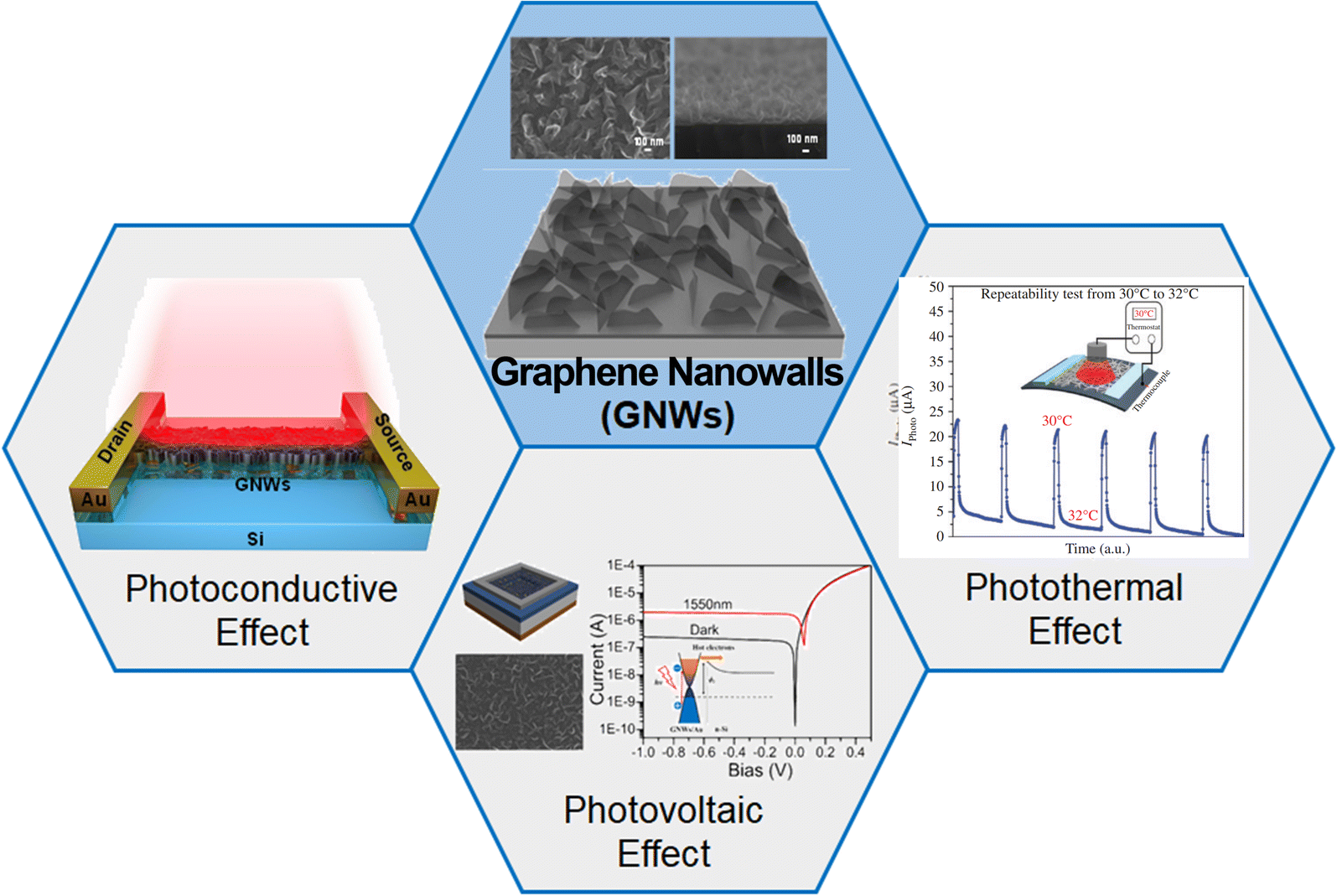 | ||
| Fig. 1 Photodetectors based on GNWs. Copyright © 2021, American Chemical Society. Copyright © 2017, Royal Society of Chemistry. Copyright © 2018, De Gruyter. | ||
2.1 Growth mechanism and experimental preparation of GNWs
GNWs are primarily fabricated using CVD technology, similar to the preparation methods of graphene, carbon nanotubes, and diamond thin films. Although some reports have employed magnetron sputtering42 or plasma-enhanced atomic layer deposition (PEALD) techniques,37 these are not mainstream methods. To obtain GNWs, a mixture of methane (CH4) and hydrogen (H2) or argon (Ar) is typically used as the carbon source in CVD, with high-density plasma essential for decomposing H2 and CH4. Commonly used plasma generation methods include microwave plasma,51,59,63 radio frequency plasma,74,77–81 electron beam excited plasma,82 and helicon wave plasma.83 This paper mainly introduces the growth mechanism analysis and experimental preparation of GNWs using radio frequency plasma-enhanced chemical vapor deposition technology (RF-PECVD). Plasma sources, as a type of high-energy particles, provide energy for the decomposition of carbon sources and the vertical growth of graphene, promoting the reaction. Firstly, carbon source precursors undergo inelastic collisions with electrons under the influence of plasma, forming carbon radicals, ions, and other carbon products. Secondly, plasma can generate a relatively high chemical potential gradient near the substrate surface through ion focusing effects. Simultaneously, plasma can increase the temperature of the upper surface, and the diffusion barrier of carbon atoms is reduced under the influence of the electric field. Consequently, PECVD has unique advantages in material preparation: low deposition temperature, no catalytic requirement for growth substrates, and strong controllability of material preparation. PECVD has thus become a common method for the preparation of GNWs. However, the introduction of plasma makes the growth process of GNWs extremely complex, fundamentally different from the preparation of graphene thin films using CVD. Therefore, it is necessary to conduct an in-depth analysis of the growth mechanism of GNWs to lay the foundation for subsequent material preparation and device optimization design.At present, researchers have conducted extensive and in-depth studies on the growth mechanism of GNWs, particularly the nucleation and induction processes of vertical graphene nanoplates. Unfortunately, due to the differences in preparation conditions and substrates, there is no unified understanding of the growth mechanism of GNWs. Mineo Hiramatsu and colleagues from Meijo University in Japan have analyzed the growth process of GNWs.42 According to their theoretical framework, the first step involves the decomposition of CH4 into carbon radicals CHx (x = 0, 1, 2, 3) at a relatively low temperature (500–800 °C) under the joint action of plasma and heating sources, which are then adsorbed onto the substrate surface to form a thin amorphous carbon layer. Plasma irradiation further excites and induces the amorphous carbon thin film, generating open dangling bonds on the surface, i.e., the formation of nucleation sites. In the second step, the adsorbed carbon-active species migrate on the substrate surface, forming carbon nanoislands. Plasma continuously decomposes methane, and carbon radicals are further adsorbed at the nucleation site, forming disordered, random, and undirected graphene nanoplate layers. These dangling bonds serve as nucleation sites for the vertical growth of graphene. In the third step, these random graphene nanoplate layers are more inclined to grow vertically under thermodynamic equilibrium, exhibiting faster growth rates and more defects. Adsorbed carbon radicals grow rapidly along the edges of the flat layers, while lateral stacking growth is largely suppressed, resulting in vertically grown, wall-like graphene. In the fourth step, when the boundaries of the vertical graphene platelet structures are filled with dangling bonds, the boundaries close, forming folded, seamless edges, and vertical graphene growth ceases. At the same time, due to plasma etching, closed boundaries are etched, forming new boundaries, i.e., secondary nucleation growth.77
In 2016, K. Davami and colleagues conducted a novel investigation and interpretation of the growth mechanism of GNWs,89 focusing on a comprehensive analysis of the buffer layer during the early stages of growth. In fact, the buffer layer is a common phenomenon in GNWs, with the amorphous carbon thin layer described by Y. H. Wu and M. Zhu being the most prevalent type of buffer layer.73,84 Through experimental preparation, K. Davami et al.89 confirmed the presence of the buffer layer and characterized its composition and microstructure. The buffer layer, situated between the substrate and vertically-oriented graphene, is approximately 20 nm thick and primarily composed of amorphous (or non-crystalline) carbon and graphene layers, including some lattice-mismatched graphene layers. Under the influence of high-energy plasma, vertical graphene grows from the mismatched defects in the buffer layer. In 2016, L. X. Zhang and colleagues from Harbin Institute of Technology conducted further research on the buffer layer and the growth process of vertical graphene.58 The amorphous carbon buffer layer grows parallel to the substrate, containing numerous layered graphite or graphene nano-layers. Under plasma induction, a significant number of defects are generated, leading to vertical graphene growth from defect sites. The vertically grown graphene layers exhibit numerous edge defects, inducing the formation of new graphene layers parallel to the pre-existing vertical graphene, resulting in wall-like graphene nanoplates or GNWs.
Another important characteristic of GNWs is the conical structure of the vertical graphene nanoplate layers, with the tip consisting of 1–3 layers of graphene and the base approximately 10 layers. Rümmeli et al. analyzed and experimentally validated this phenomenon based on the edge-gradient diffusion theory.53,58,75 In the vertical graphene region, active carbon atoms tend to aggregate at the central tip under the induction of electric fields and plasma, while carbon atom diffusion concentrations on both sides are lower, leading to a faster growth rate at the tip. This further confirms that the growth process of GNWs is defect-induced, with plasma playing a crucial role. Additionally, substrate properties, carbon source content, temperature, pressure, and plasma power all have constraining effects on the morphology, growth rate, and quality of GNWs during the growth process.42,73,74 The authors have conducted systematic research on these factors in previous studies.74
During the authors' investigation, the growth process of GNWs generally followed the mechanism outlined above, encompassing four main stages, as illustrated in Fig. 2: (1) carbon source dissociation under plasma and high temperature, (2) formation of a layered amorphous carbon buffer layer on the substrate, (3) generation of vertical growth nucleation sites on the buffer layer surface under plasma action, and (4) vertical growth of graphene from the nucleation sites to form GNWs. However, the growth mechanism exhibits some degree of variation depending on the substrate. This variation mainly lies in the formation of the buffer layer and its induction process for vertical graphene. It was found that the buffer layer of GNWs on silicon surfaces exhibits a distinct horizontal graphene layer structure, leading to poor adhesion between the GNWs and the substrate. No apparent buffer layer was observed for GNWs grown on diamond-like thin films. The morphology distribution of conformally grown GNWs on micro/nanostructures showed significant differences, especially for nanostructures with large aspect ratios. The growth of GNWs on single-crystal germanium surfaces involved a simultaneous etching process on the germanium substrate, exhibiting a distinct growth mechanism compared to existing materials.
 | ||
| Fig. 2 Growth mechanism of GNWs. (a) Dissociation of carbon–hydrogen bonds by plasma; (b) formation of the buffer layer; (c) nucleation of vertical graphene; (d) growth of GNWs. | ||
2.2 Experimental preparation of GNWs
GNWs materials are commonly prepared using RF-PECVD techniques. Fig. 3(a) shows a schematic of the PECVD equipment, where the RF and temperature zones are separated and the RF zone is located at the gas inlet, facilitating methane dissociation and carbon atom deposition. The substrate is placed at the center of the temperature zone, and the GNWs are deposited on the substrate surface by coordinating the mechanical pump and RF with the temperature zone to control the substrate temperature. As depicted in Fig. 3(b), the fabrication of GNWs encompasses five distinct stages: substrate preparation, temperature elevation, annealing, growth, and cooling.85,86 First, the growth substrates, such as silicon and germanium, are cleaned and placed at the center of the PECVD tube furnace. Air is removed from the growth chamber using a mechanical pump and repeated purging with gas. Second, a heating program is set, including heating rate, time, and sectional divisions. H2 is introduced with a flow rate of 10 sccm, the mechanical pump remains constantly on, and the chamber pressure is adjusted to ∼50 Pa. The target temperature is set to 700–750 °C with a heating duration of 40 minutes. Third, annealing is performed at 700–750 °C for 30–60 minutes to further remove impurities and internal stresses, facilitating the subsequent growth of GNWs. Fourth, the temperature is raised to the growth temperature of 750–800 °C, the ratio of carbon source to hydrogen gas is adjusted (CH4![[thin space (1/6-em)]](https://www.rsc.org/images/entities/char_2009.gif) :H2 = 6:4 sccm), the RF power is turned on, and the reflected power is minimized. Appropriate RF power (150–250 W) and growth duration are selected for growth. Finally, after the growth is complete, the RF power and methane gas source are turned off sequentially, the hydrogen gas flow rate is adjusted to 15 sccm, and the furnace lid is opened to rapidly cool the system to room temperature. The sample is then removed after exhausting the hydrogen gas. The thickness and growth rate of GNWs can be controlled by adjusting the RF power, growth temperature, and carbon source amount, with growth parameters being modified according to different materials and requirements.
:H2 = 6:4 sccm), the RF power is turned on, and the reflected power is minimized. Appropriate RF power (150–250 W) and growth duration are selected for growth. Finally, after the growth is complete, the RF power and methane gas source are turned off sequentially, the hydrogen gas flow rate is adjusted to 15 sccm, and the furnace lid is opened to rapidly cool the system to room temperature. The sample is then removed after exhausting the hydrogen gas. The thickness and growth rate of GNWs can be controlled by adjusting the RF power, growth temperature, and carbon source amount, with growth parameters being modified according to different materials and requirements.
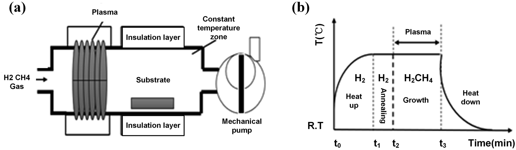 | ||
| Fig. 3 Growth process of GMWs. (a) Schematic diagram of RF-PECVD equipment for the growth of GNWs. (b) Schematic illustrating the preparation process of GNWs. | ||
3. Physical properties of GNWs
In order to validate the applicability of GNWs in photodetectors, researchers conducted a series of characterizations on the material properties. This primarily included using scanning electron microscopy (SEM), transmission electron microscopy (TEM), atomic force microscopy (AFM), and Raman spectra to characterize the microstructure and thin film quality of GNWs. Infrared spectra were employed for spectral absorption characterization, while four-point probe resistivity measurements were utilized for testing electrical conductivity. Additionally, nanoindentation/scratch tests were conducted to characterize the interfacial adhesion.3.1 Morphological analysis of GNWs
To better understand the growth mechanism and process of GNWs, microstructural characterization and analysis were performed on thin films with varying thicknesses. Fig. 4(a)–(d) presents the SEM surface morphology images of GNWs grown for 15, 30, 45, and 60 minutes, respectively. As the growth time progresses, the growth of GNWs exhibits distinct stages. In the initial stage, vertical graphene nanosheet structures, i.e., wall-like vertical edge structures, begin to grow from the nucleation sites on the buffer layer surface. With time, the density of vertical graphene increases, the edges become larger, and the height also increases. Further, upon reaching a certain stage, the edges fold or close. If the growth time is extended further, secondary nucleation occurs on the top graphene nanosheets, leading to the growth of a second layer of GNWs. As shown in Fig. 4(e)–(h), the cross-sectional SEM images reveal that the thickness of GNWs increases linearly from 330 nm to 830 nm as the growth time extends. As observed in the SEM images, the GNWs films exhibit a fluffy, porous morphology with vertically-aligned graphene nanosheets interlacing with one another. This interlocking structure provides a wealth of defect sites while simultaneously forming a unique conductive network, benefiting the electrical and mechanical stability.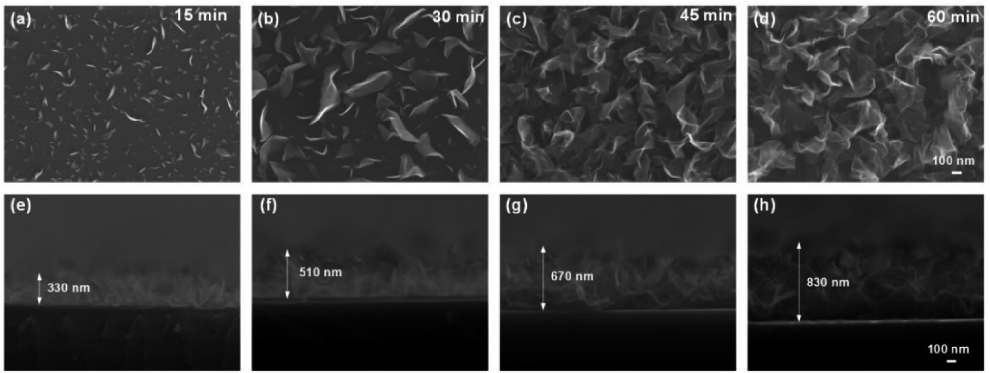 | ||
| Fig. 4 SEM images of GNWs with different growth time. (a)–(d) Top-view images; (e)–(h) cross-sectional images. | ||
To characterize the microstructure of the GNWs at the nanoscale, high-magnification TEM was employed. Fig. 5(a) further confirms the interlocking structure of the GNWs, while Fig. 5(b) reveals that an individual sheet within the GNWs is composed of multiple graphene layers (∼10 layers). Moreover, the vertical graphene sheet structures exhibit a pronounced conical configuration, with the number of graphene layers showing a gradient variation.
 | ||
| Fig. 5 TEM images and Raman spectra of GNWs. (a) Low magnification; (b) high magnification. (c) SAED pattern of the area indicated by white circle in MLG nanowalls; Copy right © 2012, Elsevier Ltd. (d) Raman spectra of GNWs and graphene film; Raman spectrum of MLG nanowalls grown for 60 min excited by (e) 633 nm and (f) 514 nm lasers. Copy right © 2012, Elsevier Ltd. | ||
Raman spectroscopy, a prevalent method for characterizing graphene and related materials' properties, serves as an essential basis for determining the quality, layer count, and defects in carbon nanomaterials such as graphene films and GNWs. A confocal micro-Raman spectrometer with a laser wavelength of 532 nm was used to analyze the GNWs. Fig. 5(d) presents the Raman spectra of single-layer graphene and GNWs, both exhibiting 2D peaks and G peaks at 2680 cm−1 and 1580 cm−1, respectively, indicating that the GNWs are composed of graphene nanosheets. Notable distinctions are: (i) a prominent defect peak D near ∼1350 cm−1 in the GNWs, with peak intensity higher than the 2D and G peaks; (ii) the presence of a D′ peak near the D peak in the GNWs. The D peak reflects defects and crystal disorder, while the D′ peak is associated with graphene edges. These results suggest that the GNWs comprise multiple layers of graphene with numerous defects and edge structures.87 Raman spectroscopy is highly sensitive to the quality of GNWs, and variations in the fabrication process can result in noticeable differences in the spectra. The stability of the PECVD process can also be evaluated through Raman spectroscopy, especially the sensitivity of the defect peak D height to the process. Currently, GNWs prepared via PECVD exhibit numerous defects, hindering the realization of high-performance optoelectronic devices.
3.2 Optical properties of GNWs
GNWs exhibit exceptional broadband light absorption, with a spectral absorption range spanning from visible light to infrared and terahertz wavelengths.69,77 Stanislav Evlashin and colleagues from Lomonosov Moscow State University conducted a systematic characterization of the optical absorption properties of GNWs of varying thicknesses, covering visible light to far-infrared wavelengths.77 Their experimental results demonstrate that 1 μm thick GNWs achieved an absorption rate of 96% to 99% within the 0.4 to 10 μm wavelength range. Moreover, the reflectance of GNWs decreased as their thickness increased. Evlashin and his team subsequently calculated the refractive index and absorbance of GNWs using the obtained infrared spectra. To obtain the broadband infrared spectral properties of GNWs, a Fourier-transform infrared/near-infrared spectroscopy system was employed. Four GNWs films with different thicknesses, grown at different times, were tested using intrinsic silicon, which is transparent to infrared, as the growth substrate for the samples. Intrinsic silicon was used as the testing background for subtraction during analysis. As depicted in Fig. 6, the transmittance curves of the GNWs with varying thicknesses within the infrared wavelength range are shown. Evidently, as the thickness of GNWs increased, the infrared transmittance gradually attenuated. With a growth time of 60 minutes, the transmittance dropped below 50%, signifying that GNWs possess superior infrared absorption properties compared to graphene films. This exceptional infrared absorption performance makes GNWs promising candidates for applications in the field of infrared detectors. The outstanding optical absorption properties of GNWs can be attributed to their unique structure. The vertically-aligned graphene nanosheets exhibit a conical thickness configuration in the height direction, forming a gradient refractive index and creating light-trapping structures at the nanoscale, which ultimately results in favorable optical absorption characteristics.69,77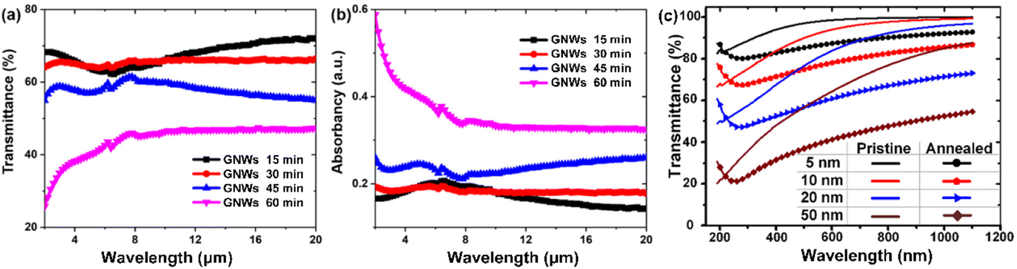 | ||
| Fig. 6 Absorption spectra of GNWs with different growth time. (a) Transmittance; (b) absorbancy; (c) optoelectronic properties of the DLC interlayer with different thicknesses before and after annealing. Copyright © 2021, American Chemical Society. | ||
3.3 Electrical properties of GNWs
GNWs exhibit metallic-like electrical properties, similar to those of graphene films. However, the presence of numerous defects on the surface of GNWs leads to high carrier concentrations and low carrier mobilities. Therefore, from an electrical performance perspective, the current electrical properties of GNWs are insufficient to compete with those of graphene films. As shown in Fig. 7, the sheet resistance of GNWs decreases from 550 Ω □−1 to 240 Ω □−1 as the growth time increases. Although the thickness of GNWs (several hundred nanometers) is significantly greater than that of single-layer graphene (0.34 nm), their sheet resistance performance does not display a distinct advantage. By calculating the conductivity of the film as γ = 1/(R□ × h), where R□ represents sheet resistance and h denotes the film thickness, the conductivity of GNWs is found to be ∼5 × 10⁴ S m−1. There is slight fluctuation in the conductivity for different thicknesses, which is attributed to differences in defect concentrations and film thickness measurement errors in GNWs films grown at different times. In comparison to graphene films with a conductivity of ∼106 S m−1, the conductivity of GNWs is two orders of magnitude lower. According to the calculation formula for conductivity and mobility, γ = nqμ (where μ represents carrier mobility), it can be inferred that the conductivity is proportional to carrier mobility; therefore, GNWs exhibit relatively lower carrier mobility than graphene films. Plasma atmosphere-induced graphene nanosheet alignment leads to abundant nanocrystalline domains, edges, defects, and even amorphous carbon on the surface, resulting in significant electron scattering and obstructed charge carrier transport, thus reducing conductivity. Electrochemical impedance spectroscopy (EIS) has been widely used to study the conductive capability of the electrodes in the system of photoelectric response. Nyquist plots in Fig. 7(f) show the conductivity of GWs and CdS-GWs electrodes in the light illumination. It explicitly indicates that the conductivity of the GWs electrode is lower than that of the CdS-GWs electrode in the light.88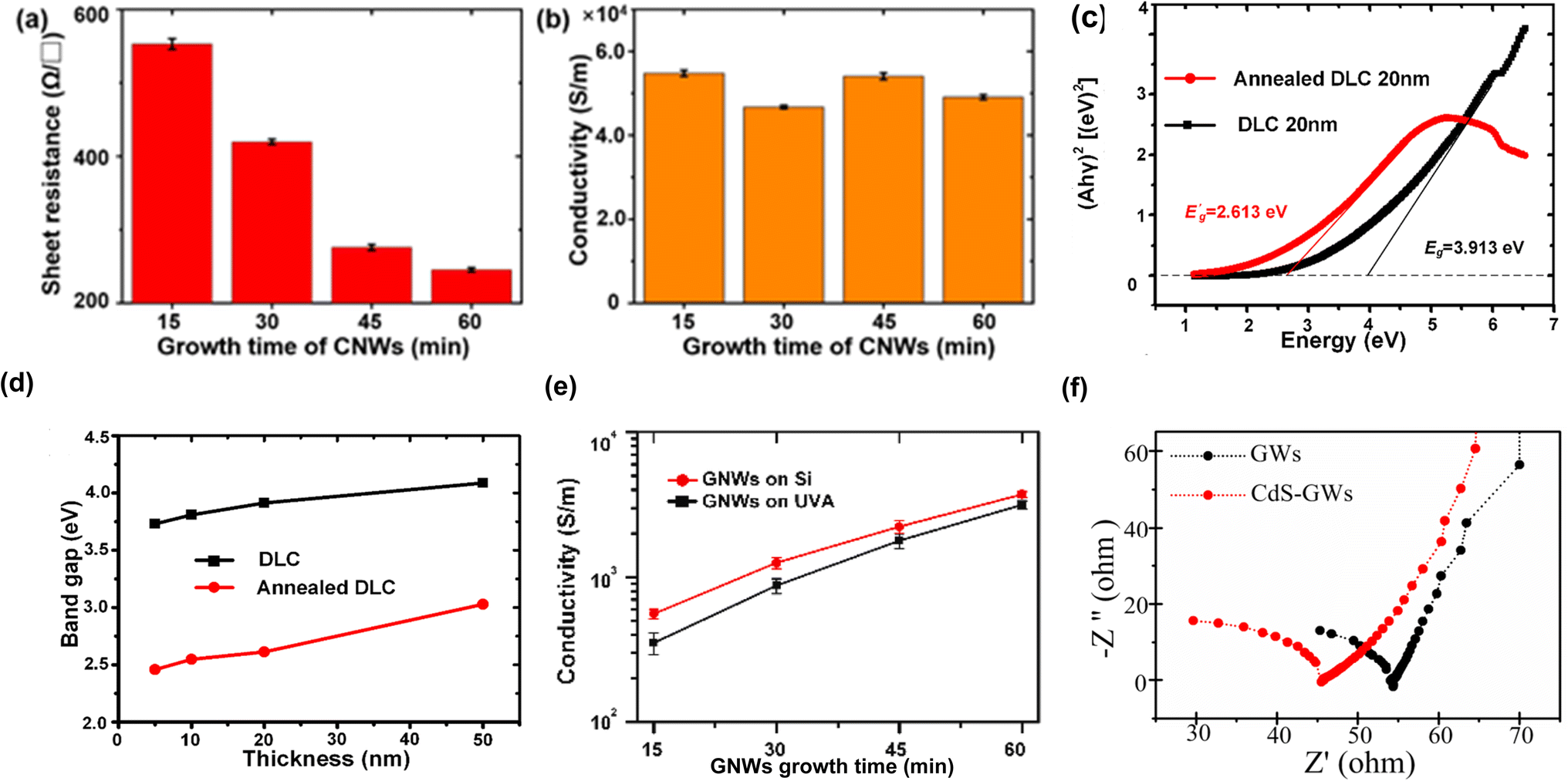 | ||
| Fig. 7 Sheet resistance (a) and conductivity (b) of GNWs; (c) plots of absorption curves calculated from the Tauc method for DLC film with different thicknesses; (d) band gap of DLC films with different thicknesses with and without annealing; Copyright © 2021, American Chemical Society. (e) The conductivity of a GNWs/Si and a GNWs/UVA hybrid film. © 2022 Elsevier B.V. All rights reserved. (f) Nyquist plots of EIS spectra recorded for the GWs and CdS-GWs (160 cycles) electrodes under the visible-light illumination (100 mW cm−2), in the electrolyte of 0.1 M Na2S. Copyright © 2015 Elsevier B.V. | ||
3.4 Mechanical properties of GNWs at interfaces
GNWs are porous, fluffy, nano-thin film materials, exhibiting markedly different mechanical behavior compared to conventional thin film materials. The vertical lamellar structure presents immense challenges for mechanical property testing. Research on the mechanical properties of GNWs is relatively scarce, with only two reports from the research group of K. Davami at the University of Pennsylvania.89,90 Kevin and colleagues conducted systematic tests and analyses on the elastic modulus and stiffness coefficients of GNWs using nanoindentation, and explored the reinforcement effects of atomic layer deposition (ALD) of nanoscale alumina and ion beam/fluorination treatments on GNWs mechanical properties. During the experiments, Kevin found that the elastic modulus of GNWs exhibited a negative correlation with the applied force, which is contrary to traditional force–displacement curves. For vertically grown graphene nanosheets, the indenter head in the initial stage caused bending deformation of the nanosheets, and the sparse, porous distribution of GNWs led to significant deviations in the test results. The elastic modulus of GNWs ranged from 10 to 100 MPa, classifying them as low-modulus materials.From a device application perspective, the bonding strength between thin film materials and substrates directly impacts device processability, stability, and reliability. The interfacial mechanical properties of GNWs with silicon, germanium, and other semiconductor wafer substrates are critical for the design and optimization of GNWs/semiconductor heterojunction photodetector devices. During photodetector fabrication, GNWs undergo a series of process steps such as photolithography, development, etching, stripping, and cleaning, presenting even greater challenges for micro/nanostructures with small linewidths. Experiments revealed that GNWs grown on silicon substrates exhibited weak interfacial bonding, leading to layer separation during cross-sectioning. As shown in Fig. 8(a), the cross-sectional scanning electron microscopy (SEM) image of the GNWs/silicon interface clearly shows the layer separation from the buffer layer on the silicon substrate, with the vertical graphene nanosheets and buffer layer distinctly visible. Furthermore, during the micro/nano patterning process of GNWs, the GNWs strips were prone to detachment and peeling, as shown in Fig. 8(b). Evidently, the interfacial mechanical properties of GNWs are insufficient to meet the application requirements in photodetectors, necessitating optimization and improvement in device design and fabrication processes. GNWs exhibit relatively weak interfacial bonding. The buffer layer at the base of the GNWs presents a horizontal layered structure, without bonding to the substrate, instead relying on van der Waals forces, which results in weak interface bonding between the buffer layer and the substrate. Based on this relatively weak bonding strength, direct transfer of GNWs can be achieved using polydimethylsiloxane (PDMS). However, for photodetectors, such interfacial mechanical properties would be a critical drawback. Introducing interface engineering to enhance interfacial bonding strength would effectively improve the compatibility of GNWs with micro/nano fabrication processes.
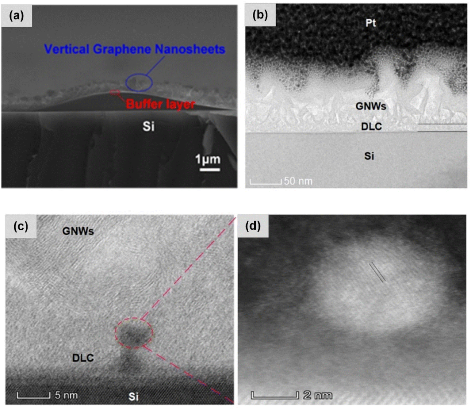 | ||
| Fig. 8 Interface adhesion between GNWs and silicon substrate. (a) Cross-sectional SEM image of Si/GNWs; (b) micropattern of Si/GNWs. (c) and (d) high-magnification cross-sectional TEM images of Si/DLC/GNWs. Copyright © 2021, American Chemical Society. | ||
3.5 Thermodynamic characteristics of GNWs
For GNWs, the large optical phonon energy of graphene is ∼200 meV,91,92 and the mismatch ratio of Fermi velocity and acoustic wave velocity (VF:Vs) reaches 100, indicating that intrinsic phonons can only scatter within a limited phase space. These characteristics result in electron–phonon coupling in graphene that is considerably weaker compared to other material systems.93 The temperature of photogenerated hot carriers (Te) is higher than the lattice temperature and can be maintained for several picoseconds. Consequently, hot carriers attain equilibrium with the lattice temperature through scattering with acoustic phonons.94,95 Although disorder-induced collisions can significantly accelerate carriers,96–98 this equilibrium process can still be completed within a few nanoseconds,94 enabling the photothermoelectric (PTE) effect to be utilized for ultrafast graphene detectors. Graphene with a specific surface area possesses a small volume and low density of states, resulting in a low heat capacity (Ch), allowing graphene-based bolometers to achieve rapid response. Due to the small Fermi surface of graphene phonons, cooling hot electrons with acoustic phonons is relatively inefficient, while cooling with optical phonons requires a higher Te (kB Te > 0.2 eV). Consequently, the responsivity (Rh) is relatively high, providing graphene with an increased sensitivity for radiation heat measurement.99
As a semimetal, graphene serves as an excellent platform for converting photons into hot carriers,100 efficiently generating a hot carrier atmosphere. Graphene exhibits strong electron–electron interactions, causing carrier thermalization within 50 fs,101,102 with a significant portion (>50%) of the initial energy of photoexcited carriers contributing to the formation of thermalized electrons. Utilizing this characteristic, the photogenerated hot carrier excitation effect can be employed, allowing the scattering of photogenerated carriers and intrinsic metallic carriers to yield a portion of thermalized electrons with elevated temperatures and energies above the barrier, thus enabling incident low-energy photons to excite electrons into the conduction band and generate photocurrents. Therefore, under continuous-wave excitation,103 these thermalized carrier temperatures can be substantially higher than the phonon temperature (Te > Tph). Furthermore, the tunability of graphene's Fermi energy allows for the control of the Schottky barrier height, which, when combined with high hot carrier temperatures, can achieve high thermal emission efficiency. Due to these reasons, GNWs are considered highly efficient and tunable ideal materials for photothermionic applications.104–106
4. GNWs-based photodetectors
GNWs thin-film materials exhibit unique optoelectronic properties, and their integration with three-dimensional semiconductor wafers like silicon and germanium forms heterojunctions that balance process compatibility and efficient photodetection. This paper primarily investigates the working mechanism, device structure design, and performance optimization of photodetectors based on photoconductive GNWs/semiconductor heterojunctions. Unlike traditional photoconductive device channels, GNWs not only act as photoconductive channels for carrier transport but also contribute to the separation of photogenerated carriers by forming Schottky heterojunctions with semiconductors. Under illumination, the photogenerated carriers in silicon and germanium semiconductors modulate the conductivity of the GNWs channel, exemplifying a typical low-dimensional photonic material photogating effect. Reported GNWs-based photodetectors mainly involve photoconductive, photothermal and photovoltaic types.4.1 GNWs-based photovoltaic detectors
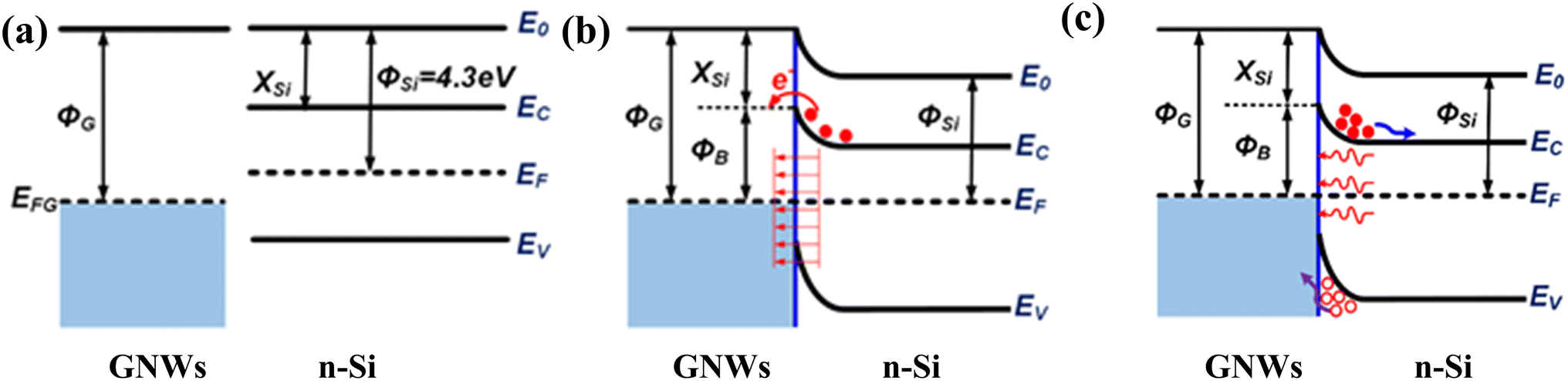 | ||
| Fig. 9 Energy band structure of GNWs/Si. (a) Uncontacted; (b) contacted; (c) schematic diagram of energy band structure of GNWs/Si heterojunction. Copyright © 2019, American Chemical Society. | ||
For GNWs/semiconductor heterojunction photodetectors, the height of the Schottky barrier plays a crucial role in determining the injection capability of photogenerated carriers, directly influencing the photogating effect and photoconductivity gain of the GNWs/semiconductor heterojunction. The height of the Schottky barrier can be calculated according to the thermionic emission theory:108
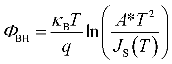 | (2.1) |
The saturation current density JS(T) can be obtained by transforming and fitting the I–V curve of the device in the photovoltaic mode. Therefore,
 | (2.2) |
In addition to thermionic emission theory, diffusion theory is also commonly used to analyze Schottky barrier potentials. Diffusion theory generally corresponds to situations where the barrier width is much larger than the average electron mean free path, while thermionic emission theory applies when electron energy is sufficiently high to pass freely through the potential barrier region. For graphene/silicon Schottky junctions, the average electron mean free path is of the same order of magnitude as the barrier width, making thermionic emission theory applicable.109 The Schottky junction formed by graphene and silicon is located at the silicon interface, and most of the photogenerated carriers excited by silicon absorbing photons are in the Schottky potential barrier, which can be effectively separated by the built-in electric field. The separated holes are quickly collected by graphene, thus achieving high responsibility and response speed. GNWs possess similar properties to graphene, and the above thermionic emission theory can be employed for analysis. However, the layered buffer layer of GNWs limits the rapid transmission and collection of photogenerated carriers, and the substantial absorption depth of bulk silicon leads to excessively long transmission paths for photogenerated carriers, further inhibiting carrier transport. Therefore, the interface optimization and design of GNWs/semiconductor heterojunctions are of paramount importance for enhancing the performance of photodetectors.
 | ||
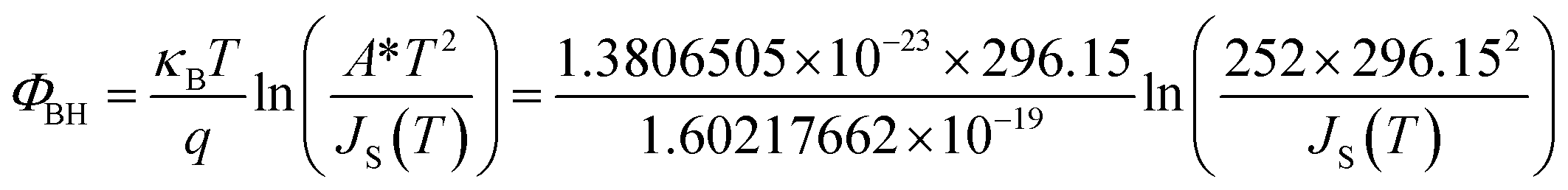
| Fig. 10 GNWs-based photovoltaic detectors. (a) Schematic representation of the GNWs/Si heterojunction detector structure; (b) illustration of the energy band diagram of the device; (c) device response under 8–14 μm laser excitation; (d) photocurrent response of the device at varying optical power levels; (e) response time characteristics of the device; (f) noise current associated with the device. Copyright © 2017, Royal Society of Chemistry. | ||
In 2019, L. Li and colleagues at Beijing University of Technology directly grew GNWs on lightly doped n-type Si via PECVD.110 By avoiding the catalyst or transfer process, the Schottky heterojunction exhibited a higher composite interface. Under 792 nm illumination, a switching ratio of nearly 105 was achieved, realizing a specific detectivity of 7.85 × 106 cm Hz1/2 W−1. Simultaneously, the device demonstrated a responsivity of 12 mA W−1 for near-infrared 1550 nm at room temperature. The device structure and performance are shown in Fig. 11. To improve the heterojunction interface between GNWs and Si, researchers have made numerous attempts. In 2019, X. Liu and others introduced Au nanoparticles before growing GNWs on n-Si via PECVD.111 This not only enhanced the absorption rate but also reduced the barrier height, improving both the internal and external quantum efficiency, and subsequently enhancing the performance of GNWs/Au/silicon heterojunction detectors. Utilizing the photothermal electric effect for detection, they achieved a response at the 1550 nm wavelength, realizing the highest specific detectivity at that time based on the Si–GNWs heterojunction. The device exhibited a room temperature responsivity of 138 mA W−1, a linear dynamic range of 89.7 dB, and a measured specific detectivity of 1.6 × 109 cm Hz1/2 W−1. Through the photothermal electric effect, the device could respond to mid-wave infrared and even THz wavelengths. The device structure and response are illustrated in Fig. 11(d) through (i).
 | ||
| Fig. 11 GNWs-based photovoltaic detectors. (a) Schematic illustration of the GNW heterostructure device grown on Si via PECVD; (b and c) device response at different wavelength bands; Copyright © 2019, AIP Publishing (d) schematic representation of the Si/Au/GNWs heterojunction device, incorporating Au nanoparticles on Si before the PECVD growth of GNWs; (e) variation in the device's absorption rate before and after the addition of Au; (f)–(i) photoresponse performance of the Si/Au/GNWs heterojunction detector. Copyright © 2019, American Chemical Society. | ||
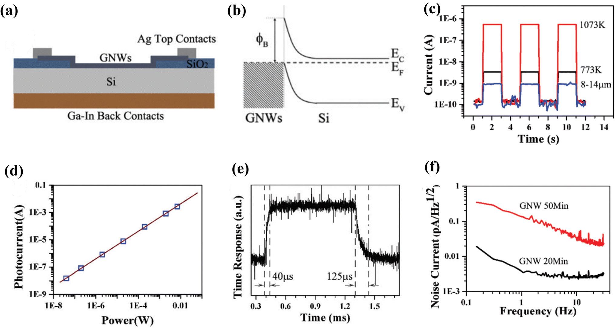
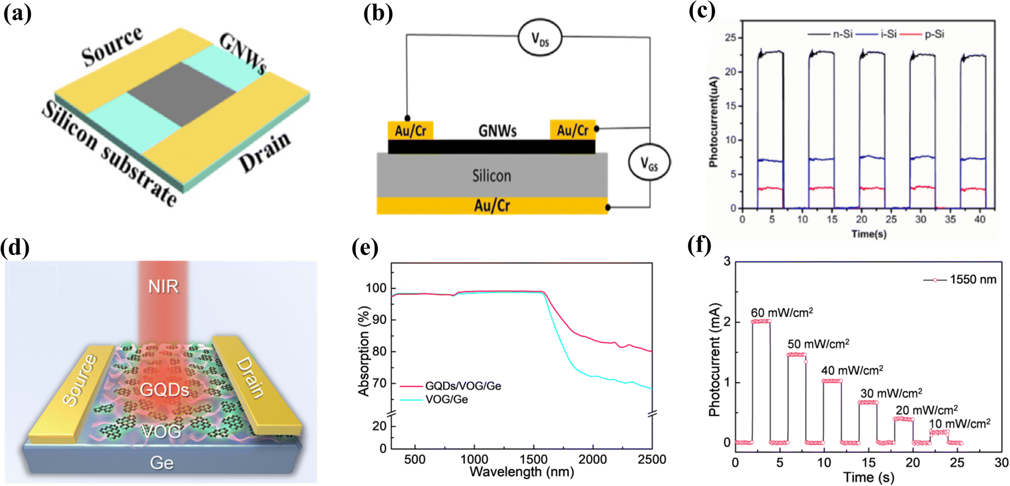
In 2021, Mingsheng Xu from Zhejiang University took an unconventional approach by directly growing GNWs on n-Si using plasma-enhanced atomic layer deposition (PEALD).37 This resulted in the development of a Si/GNW heterojunction detector with enhanced light absorption and planar electrical properties compared to those fabricated by PECVD. Due to the superior heterojunction interface, the detector exhibited improved responsivity and noise characteristics compared to PECVD devices. The device achieved a responsivity of 15 mA W−1 at a wavelength of 1342 nm and a detectivity of 1.5 × 1011 cm Hz1/2 W−1. The device structure and performance are illustrated in Fig. 12(a)–(f). By pairing GNWs with various substrates, it is possible to effectively extend the detection wavelength range from visible light to near-infrared. For instance, in 2020, M. Zhao and colleagues employed a method of first growing a 2D graphene buffer layer on a germanium (Ge) substrate, followed by the growth of 3D graphene (GNWs in this review) using PECVD.112 This process led to the fabrication of a 3D-Gr/2D-Gr/germanium heterojunction detector, which demonstrated a responsivity of 1.7 A W−1 and a detectivity of 3.42 × 1014 cm Hz1/2 W−1 at a wavelength of 1550 nm under zero-bias voltage. Moreover, the detector exhibited a response time of 68 μs, achieving superior near-infrared detection performance compared to Si/GNWs detectors on Si substrates. The device structure and performance are depicted in Fig. 12(g)–(i).
 | ||
| Fig. 12 GNWs-based photovoltaic detectors (a) fabrication process of GNWs using the PEALD method; (b) schematic illustration of the device structure; (c)–(f) photoelectric detection performance of the device; Copyright © 2021, American Chemical Society (g) schematic representation of the 3D-Gr/2D-Gr/Ge heterojunction detector structure; (h) photoelectric response currents of the 3D-Gr/2D-Gr/Ge heterojunction detector at various 1550 nm light power levels; (i) response time of the 3D-Gr/2D-Gr/Ge heterojunction detector. Copyright © 2020, American Chemical Society. | ||
4.2 GNWs-based photoconductive detectors
 | ||
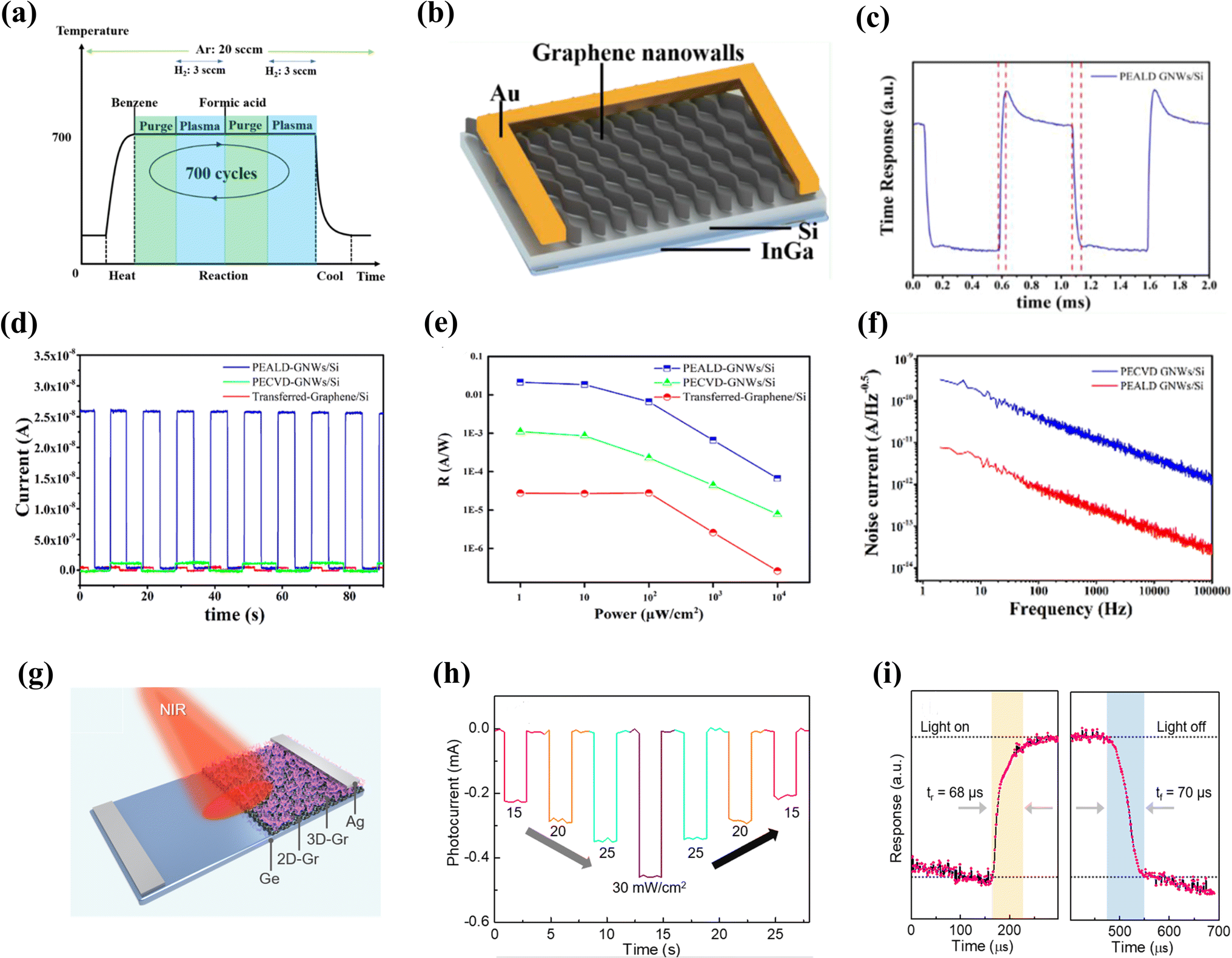
| Fig. 13 Photogating effect of low dimensional materials. (a) Photocarriers in the photosensitive layer entering the conductive channel; (b) photocarriers in the photosensitive layer gathering at the interface; (c) influence of source–drain bias voltage on photocurrent; (d) influence of gate voltage on photocurrent. | ||
At present, the photogating effect has been widely employed in low-dimensional material optoelectronic devices. Based on the materials and device types, three main categories have emerged.113 In the first type, the photosensitive layer directly contacts the channel layer, and separated photogenerated carriers can directly inject into the channel to modulate conductivity. Heterojunction photoconductive devices of graphene and other semiconductors belong to this category. In the second type, an insulating medium layer is placed between the photosensitive and channel layers, and photogenerated carriers accumulate at the interface to form a modulating gate. Such devices can achieve both large responsivities and response speeds. The third type utilizes thermoelectric materials to generate photogenerated carriers for channel conductivity modulation. However, research on this type of device is limited due to material constraints. For low-dimensional optoelectronic materials and their devices, the photogating effect organically combines two or more photoactive materials, offering greater design freedom for device structures and enabling high-performance photodetectors that capitalize on the advantages of various materials. S. Kar and colleagues provided a comprehensive analysis of the photogating effect in graphene/Si heterojunctions and the transport process of their carriers.115
Currently, most photoconductive photodetectors based on GNWs employ the photogating mechanism for photodetection, such as the commonly seen GNWs/Si heterojunction photoconductive photodetectors. The response mechanism and gain mechanism schematic of GNWs/n-Si detectors are shown in Fig. 14(a). In the absence of light, under the influence of an external bias voltage (i.e., source–drain voltage, Vds), the intrinsic carriers in the GNWs channel form a dark current (Idark) within the conductive circuit. Under illumination, photogenerated carriers are produced in silicon, as depicted in Fig. 14(b). Due to the presence of the Schottky barrier at the GNWs/Si heterojunction, electrons remain in silicon, while holes traverse the junction and inject into the GNWs conductive channel. The electrons in silicon have a longer lifetime (typically on the microsecond scale), causing them to accumulate at the interface between silicon and GNWs, forming a negative charge layer, thereby creating a gate effect on the GNWs and increasing the number of holes in the GNWs. Consequently, the conductivity of the GNWs increases, and the current passing through them increases as well, with the changing current being the photocurrent (Iph), as illustrated in Fig. 14(c). If the carrier transport speed in the GNWs channel is very fast, the injected carriers in the GNWs will be replaced multiple times before the electrons in silicon recombine, resulting in a large photoconductive gain. Swastik Kar and colleagues referred to this phenomenon as quantum carrier reinvestment (QCR). It is evident that the performance of QCR depends on the channel length, carrier mobility in the channel, and the electron lifetime in silicon; the shorter the transport channel, the higher the carrier mobility, and the longer the electron lifetime in silicon, the larger the quantum gain and the greater the responsivity of the detector. When the illumination is turned off, the holes reverse their flow back to silicon due to the termination of the carrier lifetime, where holes and electrons recombine, ending the photoresponse, as shown in Fig. 14(d). Since the injection of holes requires passing through the Schottky junction, the height of the Schottky barrier determines the number and transport speed of the injected photogenerated carriers, that is, the quantum efficiency and response speed.
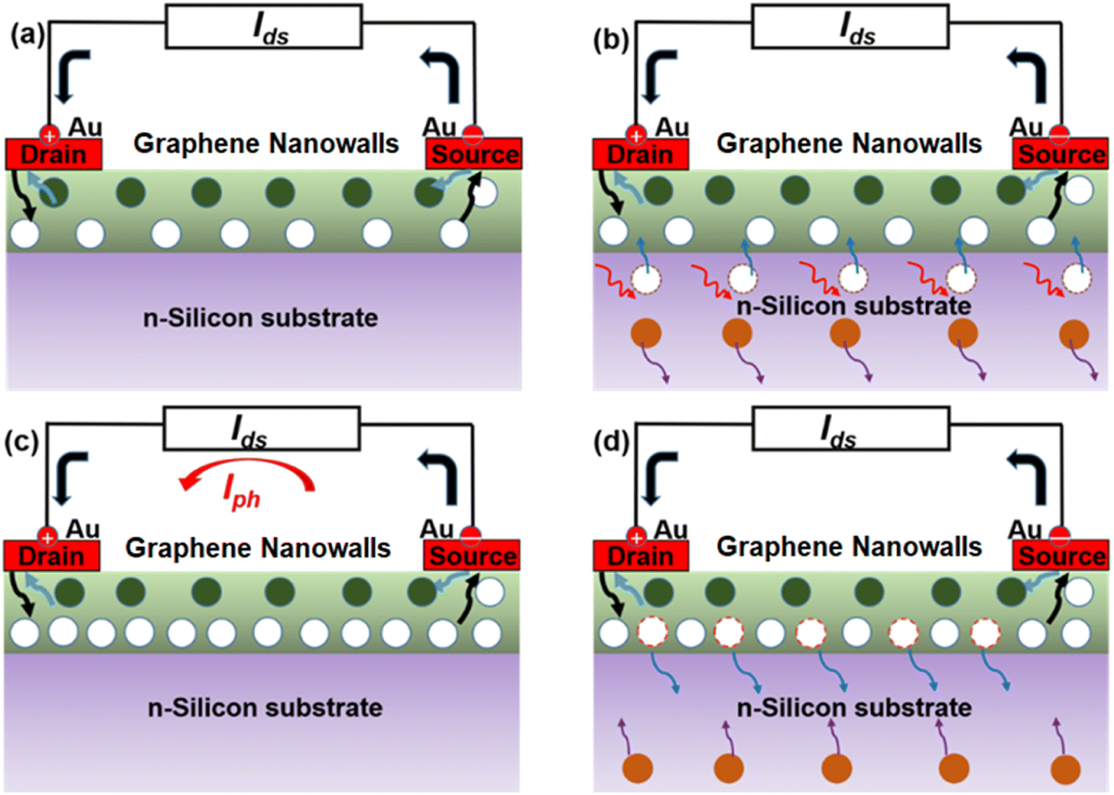 | ||
| Fig. 14 Photogating effect of GNWs/semiconductor heterojunction. (a) Dark current under an external bias due to intrinsic carriers in GNWs; (b) incident photons generate electron–hole pairs in the silicon; (c) these injected carriers gate the GNWs channel; (d) at the end of their lifetime, these carriers recombine back into silicon. | ||
In a review article by the W. Hu research group at the Shanghai Institute of Technical Physics, Chinese Academy of Sciences, on the photogating effect in low-dimensional optoelectronic materials (a specific case of photoconductivity in low-dimensional materials), it is pointed out that low-dimensional material photoconductive detectors based on the photogating effect exhibit high photoconductive gain (G) and responsivity. Moreover, the photogating effect endows optoelectronic devices with greater design flexibility, leading to high-performance photodetectors.113 Therefore, the development of photoconductive detectors based on the photogating effect will offer new opportunities for GNWs/semiconductor heterostructures.
 | ||
| Fig. 15 GNWs-based photoconductive detectors. (a) and (b) Schematic diagram of optoelectronic detector device structures using GNWs on different Si substrates; (c) photoresponse of the three devices; Copyright © 2020 Elsevier Ltd. All rights reserved. (d) Schematic diagram of the VOG/Ge heterojunction photodetector. (e) UV-NIR absorption spectra of VOG/Ge and GQDs/VOG/Ge. (f) Photoresponse properties of the GQDs/VOG/Ge device under irradiation with light of 1550 nm with variable light intensities. The applied bias is 1 V. Copyright © 2020, American Chemical Society. | ||
In addition, without utilizing the photogating effect, GNWs can also achieve photoelectric detection when prepared on insulating substrates. For instance, in 2019, G. Lan et al. grew GNWs on SnO2 substrates, exploiting the excellent conductivity of GNWs as a photogenerated carrier channel to fabricate ultraviolet absorption-enhanced photoelectric detectors,119 with the device structure and performance illustrated in the accompanying Fig. 16(a)–(c). In 2020, F. Qian and colleagues directly grew GNWs on insulating SiO2 substrates to produce pure GNWs material FET devices.120 After optimizing growth parameters, the device's responsivity significantly surpassed that of single-layer graphene devices, reaching 55 mA W−1 at 1550 nm, with the device structure and performance depicted in the accompanying Fig. 16(d)–(f).
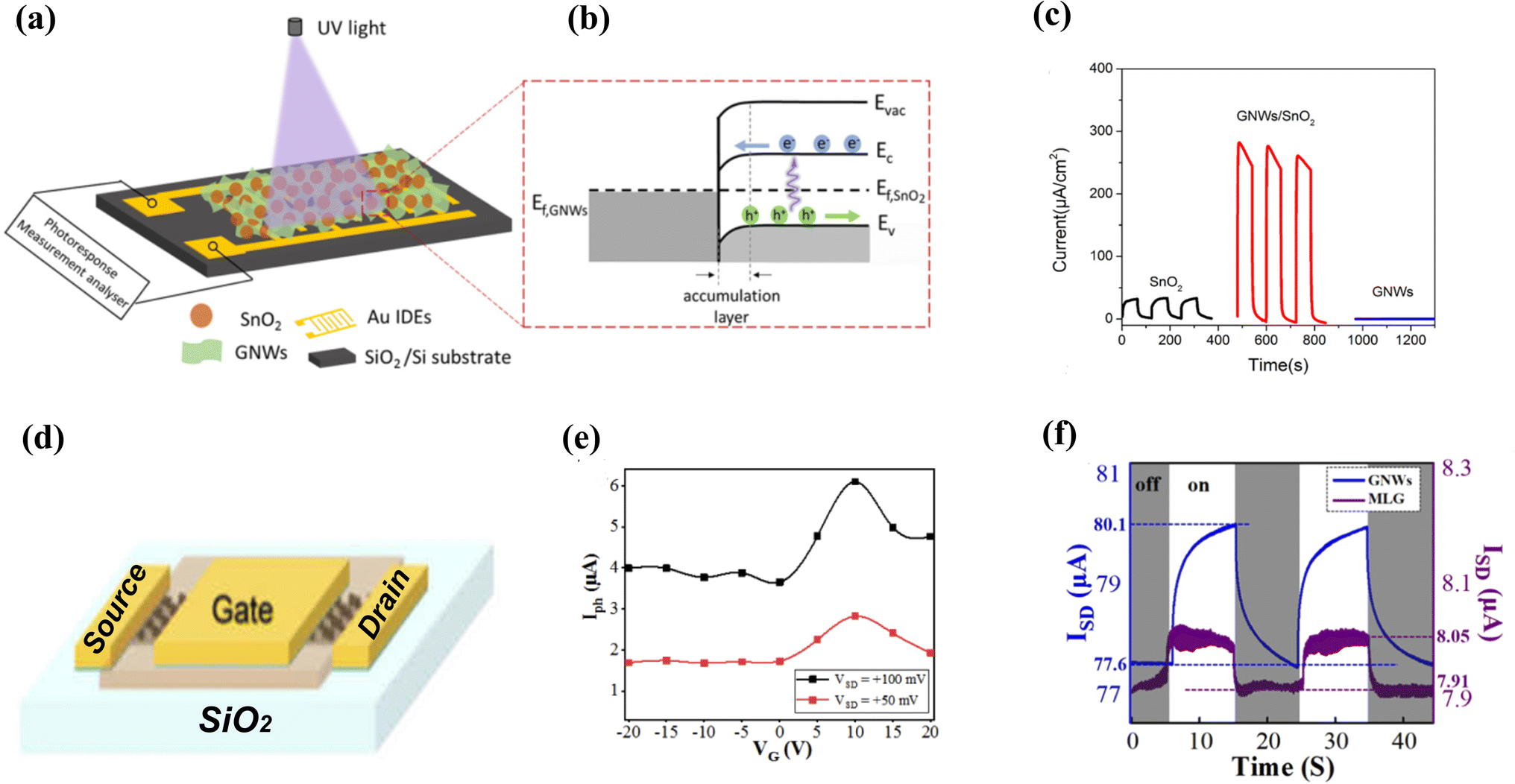 | ||
| Fig. 16 GNWs-based photoconductive detectors. (a) and (b) Device structure and energy band diagram of photoconductive devices prepared by growing GNWs on SnO2 film; (c) photoresponse performance of SnO2/GNWs devices; Copyright © 2018 Elsevier B.V. (d) Schematic diagram of FET device structure directly grown GNWs on SnO2 insulating layer substrate using PECVD; (e) photocurrent (Iph) of the GNWs photodetector at various gate voltages; (f) time-dependent Iph measurements of the GNWs photodetector and MLG photodetector working at their respective Dirac point voltage under the illumination of a 1550 nm laser, VSD = 100 mV. Reprinted with permission from120 Copyright © The Optical Society. | ||
In the conventional PECVD process of growing GNWs on Si, a horizontal buffer layer is produced, causing interface recombination issues and weakening electrical transport. In 2020, J. Yang et al. proposed the introduction of diamond-like carbon (DLC) structures during growth to improve the interface quality of Si–GNWs.44 This Si/DLC/GNWs heterojunction interface avoids the formation of a horizontal buffer layer and not only strengthens the bonding with Si through covalent bonds but also optimizes the carrier transport channel, thereby enhancing the detection performance of Si–GNWs heterojunction detectors. Compared to Si/GNWs detectors, the responsivity of Si/DLC/GNWs-based detectors increased by 1.4 times, and the composite viscosity increased by 78%. The graphitization transformation of DLC after annealing improved the carrier transport speed, and the detector's response speed also increased. The device structure and performance are shown in Fig. 17(a)–(c). In 2021, D. Zhou et al. increased the absorption of visible light in devices by incorporating organic metal halide perovskites into the porous structure of GNWs, improving the quantum conversion efficiency.45 GNWs served as a photogenerated hole collection material and exhibited outstanding carrier transport capabilities, contributing to the enhanced performance of photogating effect-based detectors. The responsivity of the detector reached 2.0 × 10³ A W−1, and the detectivity was 7.2 × 10¹⁰ Jones. The device structure and photoelectric detection performance are shown in Fig. 17(d)–(f). In a similar vein, J. Yang and colleagues at CIGIT have developed an innovative substrate design by fabricating silicon nanoholes (SiNHs) on a silicon substrate, resulting in a light-trapping structure. Subsequently, they employed PECVD to grow GNWs. This optimized substrate design effectively reduces the reflection of silicon, thereby increasing the absorption rate of the targeted wavelength from 50% to 90%. When compared to the conventional planar Si–G devices, the SiNHs–G structure demonstrates a three-fold enhancement in photoresponsivity, reaching 2720 A W−1. Furthermore, the response time of the photodetector improved from 51.3 μs to 6.2 μs. This novel approach offers a promising pathway for enhancing the performance of Si–G devices. The structural features and photodetection characteristics of the device are illustrated in Fig. 17(g)–(i).121
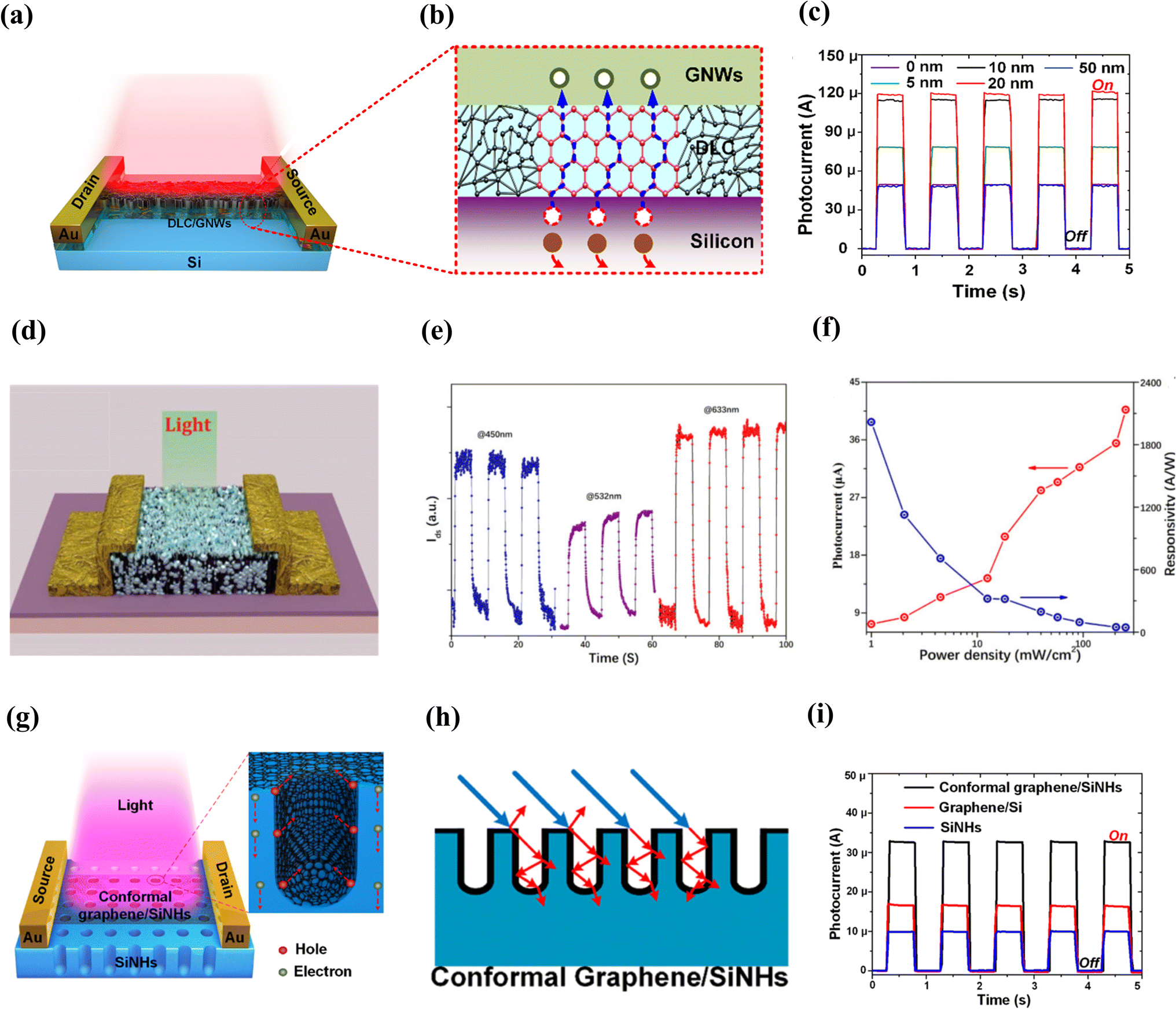 | ||
| Fig. 17 GNWs-based photoconductive detectors. (a) Schematic representation of Si/DLC/GNWs heterostructure device; (b) transformation of DLC layer to graphene-like structure after annealing; (c) infrared detection capability of Si/DLC/GNWs heterostructure device; Copyright © 2021, American Chemical Society. (d) Schematic of perovskite/GNWs photodetector device; (e) and (f) photoresponse performance of perovskite/GNWs photodetector device. Image source: “Lateral Structured Phototransistor Based on Mesoscopic Graphene/Perovskite Heterojunctions” (https://www.mdpi.com/2079-4991/11/3/641) by [Dahua Zhou*, Leyong Yu, Peng Zhu, Hongquan Zhao, Shuanglong Feng and Jun Shen] published under the Creative Commons Attribution License (CC BY) by MDPI. (g) Schematic view of the conformal graphene/SiNHs detectors. (h) Schematic view of the conformal graphene/SiNHs (i) measured photoresponse of the planar graphene/Si, SiNHs, and conformal graphene/SiNH detectors. Copyright © 2019, American Chemical Society. | ||
4.3 GNWs-based photothermal detectors
 | ||
| Fig. 18 GNWs-based photothermal detector. (a)–(c) Schematic diagram of the thermal response of GNWs/PDMS composites. Copyright © 2018, De Gruyter (d)–(f) surface morphology change of GNWs film under different temperature from 25 to 90 °C. AFM image of cracks evolution on GNWs film (50 × 50 μm) (g)–(i) the AFM cross-section of crack region (3 μm). Copyright © 2011, RSC Publishing. | ||
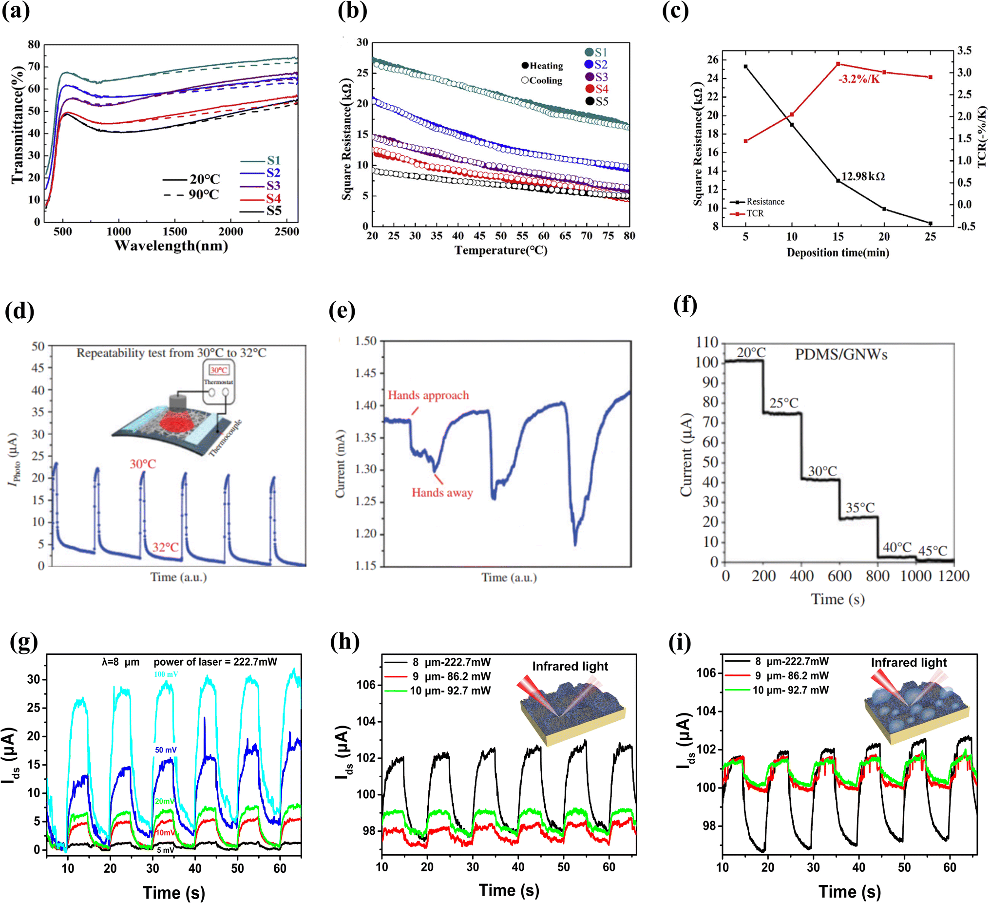 | ||
| Fig. 19 GNWs-based photothermal detector. (a) Emissivity of GNWs/VO2 devices at different GNWs deposition times (S1 = 5 min, S2 = 10 min, S3 = 15 min, S4 = 20 min, S5 = 25 min); (b) sheet resistance values of devices at different GNWs deposition times; (c) TCR and sheet resistance of optimized thickness device; Copyright © 2020 The Chinese Ceramic Society. Production and hosting by Elsevier B.V. (d)–(f) Photoresponse properties of photodetectors based on GNWs/PDMS composites; Copyright © 2018, De Gruyter. (g) The photocurrent of the GNWs/UVA detector underdifferent bias voltages at the wavelength of 8 μm at room temperature; (h) the photocurrent of the GNWs/UVA detector under different wavelengths from 8–10 μm before dripping; (i) the photocurrents of the GNWs/UVA detector under different wavelengths from 8–10 μm after dripping. Copyright © 2022 Elsevier B.V. All rights reserved. | ||
To further investigate the thermal response mechanism of GNWs/PDMS composites, atomic force microscopy (AFM) and optical microscopy have been employed to observe in situ morphological changes in the composite films under temperature variations. Upon temperature increase, significant cracks appear on the film surface, with the number of cracks increasing with rising temperature. AFM measurements of crack depth reveal values of approximately 400 nm, consistent with the thickness of GNWs, indicating that the cracks are exclusive to the GNWs film and caused by PDMS thermal expansion. Cracks divide the GNWs into discontinuous conductive films, substantially increasing film resistivity. Interestingly, when the temperature decreases, the cracks gradually disappear and return to their initial state, with the film resistance recovering to its initial value. Repeated heating and cooling cycles confirm the composite film's stability. The high TCR is attributed to two factors: the infrared radiation absorption properties of GNWs and the thermal expansion coefficient of the PDMS film. By comparing substrates with different thermal expansion coefficients (e.g., Si, PET, PDMS), it has been found that PDMS (ε = 3.0 × 10⁻⁴ °C−1) exhibits the highest TCR. Further infrared radiation response experiments demonstrate significant responses of the composite film to infrared lamps, 980 nm laser irradiation, and human body thermal radiation, indicating excellent infrared detection performance for GNWs/PDMS composites.61,122 GNWs/PDMS composite materials have shown an ultra-high TCR, providing promising potential in the field of uncooled microbolometers. However, significant challenges remain regarding the compatibility of polymer systems with silicon microfabrication processes. Device miniaturization and array fabrication processes may lead to film or device failure, making it difficult to control device and process stability. In 2023, J. Yang et al. successfully fabricated flexible infrared detectors with superhydrophobic properties by employing a two-step transfer method. In this process, GNWs were initially transferred onto a flexible PDMS substrate, followed by a subsequent transfer onto a UV-curable adhesive. The resulting detector demonstrated responsivity to long-wave infrared radiation through the thermoelectric effect, achieving room temperature photoelectric detection within the wavelength range of 8–10 μm, as depicted in Fig. 19(g)–(i).49
5. Conclusion and outlook
In summary, GNWs can be directly grown in situ on semiconductor substrates such as silicon and germanium to form heterojunction devices, and exhibit good photodetection performance compared to graphene, black phosphorus, quantum dots, etc. Other low-dimensional optoelectronic materials have better device stability and process compatibility. However, the current research on photodetectors based on GNWs/semiconductor heterojunctions is still in its infancy, and there are still a series of problems that need to be solved urgently. Table 1 presents a comparative analysis of the performance metrics including responsivity, response time, wavelength, and detectivity for photodetectors fabricated using GNWs in recent years.| Wavelength | Response time | Responsivity (A W−1) | Detectivity (cm Hz1/2 W−1) | Ref. | |
|---|---|---|---|---|---|
| GNWs/Si heterojunctions | 8–14 μm | 40 μs | 0.52 | 5.88 × 10¹³ (measured) | 80 |
| GNWs/Si Schottky junction | 635 nm | 0.14 | 46 | ||
| GNWs/Si | 792 –1550 nm | 1 | 7.85 106 | 110 | |
| GNWs/Au/n-Si heterojunction | 1550 nm to mid-wave infrared and THz | 1.38 × 10⁻¹ | 1.6 × 10⁹ (measured) | 111 | |
| Si/GNW by PEALD | 1342 nm | 1.5 × 10⁻² | 1.5 × 10¹¹ | 37 | |
| 3D-Gr/2D-Gr/germanium heterojunction | 1550 nm | 68 μs | 1.7 | 3.42 × 10¹⁴ | 112 |
| GQDs/VOG/Ge photodetector | 1550 nm | 1.06 × 10⁶ | 2.11 × 10¹⁴ | 118 | |
| GNWs FET devices | 1550 nm | 5.5 × 10⁻² | 120 | ||
| Si/DLC/GNWs heterojunction | 532 and 1550 nm | 13 μs | 2400 | 1.07 × 10¹¹ | 44 |
| CH3NH3PbIxCl3−x/GNWs | 635 nm | 50 ms | 2000 | 7.2 × 10¹⁰ | 45 |
| GNWs/silicon nanoholes | 635–1550 nm | 6.2 μs | 2720 | 1.25 × 10¹¹ | 121 |
| GNWs/PDMS films | 980 nm | 4 s | 1.15 × 10⁻³ | 1.07 × 10⁸ | 122 |
| GNWs/UVA | 8–10 μm | 2.8 × 10⁻⁵ | 49 |
5.1 Photodetection mechanism of GNWs/semiconductor heterojunction photoconductive devices
There are relatively few studies in GNWs-based photodetectors, and a systematic study of the photodetection mechanism of GNWs/semiconductor heterojunctions is lacking. In particular, photoconductive photodetectors based on GNWs/semiconductor heterojunctions have not been reported yet. It is necessary to conduct in-depth analysis on the generation, separation, transport and recombination process of photogenerated carriers in GNWs/semiconductor heterojunction, clarify the photoelectric response mechanism of GNWs/semiconductor heterojunction photoconductive device, and based on this is the design and optimization of the device structure.5.2 Interface mechanical behavior of GNWs/semiconductor heterojunction and its device process compatibility
After more than ten years of development, the research and application of GNWs involve various fields, but there is no research on the compatibility of GNWs with silicon micro-processes. For optoelectronic devices, the channel patterning and unit device integration of optoelectronic functional materials are the keys to measure their practicality. On the other hand, it was found in the experiment that the interface bonding force between the GNWs and the silicon substrate was poor, and the interface film layer was easily separated and peeled off, which limited the compatibility of the device process.5.3 Severe reflection at the GNWs/semiconductor heterojunction interface leads to low photoelectric conversion efficiency of the device
The light absorption of silicon and the photoelectric conversion efficiency of the device are limited due to the sharp reduction of light quantum entering the photosensitive layer due to the specular reflection of up to 40% on the smooth silicon surface. Moreover, the light absorption coefficient of silicon material is small, and smooth silicon requires a thickness of tens of micrometers or even hundreds of micrometers to achieve sufficient absorption of incident light, which will lead to a long diffusion distance of photogenerated carriers in deep silicon and direct recombination, which further limits the device photoelectric responsivity and response speed.5.4 Limited by the band gap of the semiconductor photosensitive layer, it is difficult to achieve broadband photoelectric response
Although GNWs have broad spectral absorption properties, their own defects lead to the direct recombination of photogenerated carriers before they are separated, making it difficult to directly achieve photoelectric response or very weak photoelectric response. The spectral response band of the GNWs/semiconductor heterojunction photodetector is mainly limited by the forbidden bandwidth of the semiconductor, and the band gap of silicon determines that the working band of the GNWs/silicon heterojunction device is difficult to further expand.Author contributions
Jun Yang: project administration, writing-review & editing, funding acquisition, supervision, conceptualization. Qi Yang: writing-original investigation. Yongna Zhang: investigation, writing. Xingzhan We: supervision, writing-editing. Hanfe Shi: project administration, writing-reviewing, funding acquisition, supervision, conceptualization.Conflicts of interest
The authors declare that they have no known competing financial interests or personal relationships that could have appeared to influence the work reported in this paper.Acknowledgements
This work was supported by the National Natural Science Foundation of China (NSFC 52175281), Youth Innovation Promotion Association of CAS (2021382). I extend my gratitude to the publishers and authors of the articles referred to in this paper, who have generously granted me free use of portions of their scientific achievements. Their contributions have facilitated the successful publication of this review article.References
- F. Hou, et al., Review on Infrared Imaging Technology, Sustainability, 2022, 14(18), 11161 CrossRef.
- X. Hu, et al., Recent developments of infrared photodetectors with low-dimensional inorganic nanostructures, Nano Res., 2022, 15(2), 805–817 CrossRef CAS.
- W.-D. Hu, et al., Recent progress on advanced infrared photodetectors, Acta Phys. Sin., 2019, 68(12), 120701 CrossRef.
- J. Liu, et al., Development of long-wavelength infrared detector and its space-based application requirements, Chin. Phys. B, 2019, 28(2), 028504 CrossRef CAS.
- X. Lu, et al., Progress of Photodetectors Based on the Photothermoelectric Effect, Adv. Mater., 2019, 31(50), 1902044 CrossRef CAS PubMed.
- B. Wang, et al., Broadband photodetectors based on 2D group IVA metal chalcogenides semiconductors, Appl. Mater. Today, 2019, 15, 115–138 CrossRef CAS.
- Z.-M. Wei and J.-B. Xia, Recent progress in polarization-sensitive photodetectors based on low-dimensional semiconductors, Acta Phys. Sin., 2019, 68(16), 163201 CrossRef.
- F.-Y. Yue, et al., Optical characterization of defects in narrow-gap HgCdTe for infrared detector applications, Chin. Phys. B, 2019, 28(1), 017104 CrossRef CAS.
- S. Bianconi and H. Mohseni, Recent advances in infrared imagers: toward thermodynamic and quantum limits of photon sensitivity, Rep. Prog. Phys., 2020, 83(4), 44101 CrossRef CAS.
- Z. Li, et al., Review on III-V Semiconductor Single Nanowire-Based Room Temperature Infrared Photodetectors, Materials, 2020, 13(6), 1400 CrossRef CAS PubMed.
- R. Ma, et al., Research Status and Prospect of Infrared Photoelectric Detection Technology (Invited), Acta Photonica Sin., 2021, 50(10), 1004006 CrossRef.
- A. Rogalski, et al., Trends in Performance Limits of the HOT Infrared Photodetectors, Appl. Sci., 2021, 11(2), 501 CrossRef CAS.
- P. Martyniuk, A. Rogalski and S. Krishna, Interband Quantum Cascade Infrared Photodetectors: Current Status and Future Trends, Phys. Rev. Appl., 2022, 17(2), 027001 CrossRef CAS.
- H. Wang, et al., Emerging Single-Photon Detectors Based on Low-Dimensional Materials, Small, 2022, 18(5), 2103963 CrossRef CAS PubMed.
- J. Zha, et al., Infrared Photodetectors Based on 2D Materials and Nanophotonics, Adv. Funct. Mater., 2022, 32(15), 2111970 CrossRef CAS.
- C. Zhang, et al., Recent Progress and Future Opportunities for Hot Carrier Photodetectors: From Ultraviolet to Infrared Bands, Laser Photonics Rev., 2022, 16(6), 2100714 CrossRef.
- J. Liu, et al., Organic and quantum dot hybrid photodetectors: towards full-band and fast detection, Chem. Commun., 2023, 59(3), 260–269 RSC.
- Q. Tang, et al., Infrared Photodetection from 2D/3D van der Waals Heterostructures, Nanomaterials, 2023, 13(7), 1169 CrossRef CAS.
- M. A. Kinch, Fundamental physics of infrared detector materials, J. Electron. Mater., 2000, 29, 809–817 CrossRef CAS.
- M. Henini and M. Razeghi, Handbook of infrared detection technologies, Elsevier, 2002 Search PubMed.
- A. Rogalski, Infrared detectors: an overview, Infrared Phys. Technol., 2002, 43(3–5), 187–210 CrossRef.
- A. Rogalski, HgCdTe infrared detector material: history, status and outlook, Rep. Prog. Phys., 2005, 68(10), 2267 CrossRef CAS.
- A. Rogalski, Recent progress in infrared detector technologies, Infrared Phys. Technol., 2011, 54(3), 136–154 CrossRef.
- A. Rogalski, History of infrared detectors, Opto-Electron. Rev., 2012, 20, 279–308 Search PubMed.
- Y. Jun, Photodetector Based on Carbon Nanowalls/Semiconductor Heterojunction, PhD thesis, University of Chinese Academy of Sciences, 2019.
- J. Kim, et al., Recent Advances in Low-Dimensional Nanomaterials for Photodetectors, Small Methods, 2023, 2300246 CrossRef PubMed.
- J. L. Pura, Optical and Electrical Properties of Low-Dimensional Crystalline Materials: A Review, Crystals, 2023, 13(1), 108 CrossRef CAS.
- W. Miao, et al., The magical photoelectric and optoelectronic properties of graphene nanoribbons and their applications, J. Mater. Chem. C, 2021, 9(39), 13600–13616 RSC.
- Z. Wang, et al., Graphene in 2D/3D Heterostructure Diodes for High Performance Electronics and Optoelectronics, Adv. Electron. Mater., 2021, 7(7), 2001210 CrossRef CAS.
- M. Ye, et al., Graphene-based mid-infrared photodetectors using metamaterials and related concepts, Appl. Phys. Rev., 2021, 8(3), 031303 CAS.
- R. Cao, et al., Mid-Infrared Optoelectronic Devices Based on Two-Dimensional Materials beyond Graphene: Status and Trends, Nanomaterials, 2022, 12(13), 2260 CrossRef CAS PubMed.
- J. Du, et al., Advances in Flexible Optoelectronics Based on Chemical Vapor Deposition-Grown Graphene, Adv. Funct. Mater., 2022, 32(42), 2203115 CrossRef CAS.
- D. A. Katzmarek, et al., Review of graphene for the generation, manipulation, and detection of electromagnetic fields from microwave to terahertz, 2D Materials, 2022, 9(2), 022002 CrossRef.
- Y. Wang, et al., Laser-Based Growth and Treatment of Graphene for Advanced Photo- and Electro-Related Device Applications, Adv. Funct. Mater., 2022, 32(42), 2203164 CrossRef.
- M.-K. Zhang, et al., Graphene/Quantum Dot Heterostructure Photodetectors: From Material to Performance, Adv. Opt. Mater., 2022, 10(24), 2201889 CrossRef CAS.
- Q. Zhou, Q. Qiu and Z. Huang, Graphene-based terahertz optoelectronics, Opt. Laser Technol., 2023, 157, 108558 CrossRef CAS.
- J. Cong, et al., Direct Growth of Graphene Nanowalls on Silicon Using Plasma-Enhanced Atomic Layer Deposition for High-Performance Si-Based Infrared Photodetectors, ACS Appl. Electron. Mater., 2021, 3(11), 5048–5058 CrossRef CAS.
- F. Huang, et al., Direct Growth of Graphene Nanowalls on Inverted Pyramid Silicon for Schottky Junction Solar Cells, ACS Appl. Energy Mater., 2021, 4(7), 6574–6584 CrossRef CAS.
- X. Tang, et al., Controllable Graphene Wrinkle for a High-Performance Flexible Pressure Sensor, ACS Appl. Mater. Interfaces, 2021, 13(17), 20448–20458 CrossRef CAS.
- Z. Wang, et al., Synthesis of Vertical Graphene Nanowalls on Substrates by PECVD as Effective EMI Shielding Materials, ACS Appl. Electron. Mater., 2022, 4(8), 4023–4032 CrossRef CAS.
- E. Bertran-Serra, et al., Temperature-modulated synthesis of vertically oriented atomic bilayer graphene nanowalls grown on stainless steel by inductively coupled plasma chemical vapour deposition, Appl. Surf. Sci., 2023, 610, 55530 CrossRef.
- H. Mineo and H. Masaru, Carbon Nanowalls: Synthesis and Emerging Applications, SpringerWienNewYork, NewYork, 2010 Search PubMed.
- E. O. Orhan, et al., 3D-graphene-laser patterned p-type silicon Schottky diode, Mater. Sci. Semicond. Process., 2021, 121, 105454 CrossRef CAS.
- J. Yang, et al., Interface Engineering of a Silicon/Graphene Heterojunction Photodetector via a Diamond-Like Carbon Interlayer, ACS Appl. Mater. Interfaces, 2021, 13(3), 4692–4702 CrossRef CAS.
- D. Zhou, et al., Lateral Structured Phototransistor Based on Mesoscopic Graphene/Perovskite Heterojunctions, Nanomaterials, 2021, 11(3), 641 CrossRef CAS PubMed.
- Q. Zhou, et al., The controlled growth of graphene nanowalls on Si for Schottky photodetector, AIP Adv., 2017, 7(12), 25317 Search PubMed.
- J. Yang, et al., High-Performance 3D Vertically Oriented Graphene Photodetector Using a Floating Indium Tin Oxide Channel, Sensors, 2022, 22(3), 959 CrossRef CAS PubMed.
- Y. H. Shen, et al., High-Performance Graphene Nanowalls/Si Self-Powered Photodetectors with HfO2 as an Interfacial Layer, Nanomaterials, 2023, 13(10), 1681 CrossRef CAS PubMed.
- Q. Yang, et al., Superhydrophobic graphene nanowalls for electromagnetic interference shielding and infrared photodetection via a two-step transfer method, Chem. Eng. J., 2023, 454, 140159 CrossRef CAS.
- Y. Ando, X. Zhao and M. Ohkohchi, Production of petal-like graphite sheets by hydrogen arc discharge, Carbon, 1997, 35(1), 153–158 CrossRef CAS.
- Y. Wu, et al., Carbon Nanowalls Grown by Microwave Plasma Enhanced Chemical Vapor Deposition, Adv. Mater., 2002, 14(1), 64–67 CrossRef CAS.
- X. Song, et al., 3-D conformal graphene for stretchable and bendable transparent conductive film, J. Mater. Chem. C, 2015, 3(48), 12379–12384 RSC.
- J. Zhao, et al., A growth mechanism for free-standing vertical graphene, Nano Lett., 2014, 14(6), 3064–3071 CrossRef CAS PubMed.
- O. Akhavan, E. Ghaderi and R. Rahighi, Toward Single-DNA Electrochemical Biosensing by Graphene Nanowalls, ACS Nano, 2012, 6(4), 2904–2916 CrossRef CAS PubMed.
- Y. Wu, et al., Carbon nanowalls and related materials, J. Mater. Chem., 2004, 14(4), 469–477 RSC.
- B. Yang, et al., Electrochemical Synthesis and Characterization of Magnetic Nanoparticles on Carbon Nanowall Templates, Nano Lett., 2002, 2(7), 751–754 CrossRef CAS.
- Y. Wu, et al., Fabrication of a Class of Nanostructured Materials Using Carbon Nanowalls as the Templates, Adv. Funct. Mater., 2002, 12(8), 489–494 CrossRef CAS.
- L. X. Zhang, et al., Understanding the growth mechanism of vertically aligned graphene and control of its wettability, Carbon, 2016, 103, 339–345 CrossRef CAS.
- P. Hojati-Talemi and G. P. Simon, Field emission study of graphene nanowalls prepared by microwave-plasma method, Carbon, 2011, 49(8), 2875–2877 CrossRef CAS.
- J. Yang, et al., Three-dimensional conformal graphene microstructure for flexible and highly sensitive electronic skin, Nanotechnology, 2017, 28(11), 115501 CrossRef PubMed.
- J. Yang, et al., Wearable temperature sensor based on graphene nanowalls, RSC Adv., 2015, 5(32), 25609–25615 RSC.
- S. Wang, et al., High field emission reproducibility and stability of carbon nanosheets and nanosheet-based backgated triode emission devices, Appl. Phys. Lett., 2006, 89(18), 183103 CrossRef.
- J. Wang and T. Ito, High-current-density electron emissions from nano-carbon films fabricated by high-power microwave-plasma chemical vapour deposition, Diamond Relat. Mater., 2005, 14(9), 1469–1473 CrossRef CAS.
- A. Malesevic, et al., Field emission from vertically aligned few-layer graphene, J. Appl. Phys., 2008, 104(8), 084301 CrossRef.
- A. T. H. Chuang, et al., Three-dimensional carbon nanowall structures, Appl. Phys. Lett., 2007, 90(12), 123107 CrossRef.
- T. Machino, et al., Synthesis of Platinum Nanoparticles on Two-Dimensional Carbon Nanostructures with an Ultrahigh Aspect Ratio Employing Supercritical Fluid Chemical Vapor Deposition Process, Appl. Phys. Express, 2009, 2, 025001 CrossRef.
- L. Giorgi, et al., Electrochemical properties of carbon nanowalls synthesized by HF-CVD, Sens. Actuators, B, 2007, 126(1), 144–152 CrossRef CAS.
- H. Wang, et al., Fabrication of a TiO2/carbon nanowall heterojunction and its photocatalytic ability, Carbon, 2008, 46(8), 1126–1132 CrossRef CAS.
- V. A. Krivchenko, et al., Carbon nanowalls: the next step for physical manifestation of the black body coating, Sci. Rep., 2013, 3, 3328 CrossRef CAS PubMed.
- Z. Zhang, et al., Hierarchical composite structure of few-layers MoS 2 nanosheets supported by vertical graphene on carbon cloth for high-performance hydrogen evolution reaction, Nano Energy, 2015, 18, 196–204 CrossRef CAS.
- O. Tanaike, et al., Lithium insertion behavior of carbon nanowalls by dc plasma CVD and its heat-treatment effect, Solid State Ionics, 2009, 180(4), 381–385 CrossRef CAS.
- E. Luais, et al., Carbon nanowalls as material for electrochemical transducers, Appl. Phys. Lett., 2009, 95(1), 014104 CrossRef.
- Y. H. Wu, et al., Carbon nanowalls and related materials, J. Mater. Chem., 2004, 14(4), 469–477 RSC.
- X. Song, et al., Direct versatile PECVD growth of graphene nanowalls on multiple substrates, Mater. Lett., 2014, 137, 25–28 CrossRef CAS.
- Y. Ma, et al., Copper-Assisted Direct Growth of Vertical Graphene Nanosheets on Glass Substrates by Low-Temperature Plasma-Enhanced Chemical Vapour Deposition Process, Nanoscale Res. Lett., 2015, 10(1), 1019 Search PubMed.
- J. Dong, et al., Control of Superhydrophilic and Superhydrophobic Graphene Interface, Sci. Rep., 2013, 3, 1733 CrossRef.
- S. Evlashin, et al., Optical and IR absorption of multilayer carbon nanowalls, Carbon, 2014, 70, 111–118 CrossRef CAS.
- T. Jiao, et al., Composite Transparent Electrode of Graphene Nanowalls and Silver Nanowires on Micropyramidal Si for High-Efficiency Schottky Junction Solar Cells, ACS Appl. Mater. Interfaces, 2015, 7(36), 20179–20183 CrossRef CAS PubMed.
- J. Liu, et al., Direct growth of graphene nanowalls on the crystalline silicon for solar cells, Appl. Phys. Lett., 2015, 106(4), 043904 CrossRef.
- J. Shen, et al., High-performance Schottky heterojunction photodetector with directly grown graphene nanowalls as electrodes, Nanoscale, 2017, 9(18), 6020–6025 RSC.
- Q. Zhou, et al., The controlled growth of graphene nanowalls on Si for Schottky photodetector, AIP Adv., 2017, 7(12), 125317 CrossRef.
- T. Mori, et al., Fabrication of carbon nanowalls using electron beam excited plasma-enhanced chemical vapor deposition, Diamond Relat. Mater., 2008, 17(7), 1513–1517 CrossRef CAS.
- G. Sato, et al., Fast Growth of Carbon Nanowalls from Pure Methane using Helicon Plasma-Enhanced Chemical Vapor Deposition, Jpn. J. Appl. Phys., 2006, 45(6), 5210–5212 CrossRef CAS.
- M. Zhu, et al., A mechanism for carbon nanosheet formation, Carbon, 2007, 45(11), 2229–2234 CrossRef CAS.
- J. Chu, et al., Study of the structural evolution and gas sensing properties of PECVD-synthesized graphene nanowalls, J. Phys. D: Appl. Phys., 2020, 53(32), 325101 CrossRef CAS.
- X. Song, et al., Direct versatile PECVD growth of graphene nanowalls on multiple substrates, Mater. Lett., 2014, 137, 25–28 CrossRef CAS.
- M. Hiramatsu, H. Kondo, and M. Hori, New Progress on Graphene Research, INTECH, Austria, 2013, pp. 235–236 Search PubMed.
- X. Song, et al., Enhanced photoelectrochemical perporties of graphene nanowalls–CdS composite materials, J. Alloys Compd., 2015, 651, 230–236 CrossRef CAS.
- K. Davami, et al., Tuning the mechanical properties of vertical graphene sheets through atomic layer deposition, Nanotechnology, 2016, 27(15), 155701 CrossRef.
- C. Lin, et al., Enhancing the stiffness of vertical graphene sheets through ion beam irradiation and fluorination, Nanotechnology, 2017, 28(29), 295701 CrossRef PubMed.
- S. Piscanec, et al., Kohn anomalies and electron-phonon interactions in graphite, Phys. Rev. Lett., 2004, 93(18), 185503 CrossRef CAS.
- M. Lazzeri, et al., Electron transport and hot phonons in carbon nanotubes, Phys. Rev. Lett., 2005, 95(23), 236802 CrossRef.
- T. Low and P. Avouris, Graphene Plasmonics for Terahertz to Mid-Infrared Applications, ACS Nano, 2014, 8(2), 1086–1101 CrossRef CAS PubMed.
- R. Bistritzer and A. H. MacDonald, Electronic Cooling in Graphene, Phys. Rev. Lett., 2009, 102(20), 206410 CrossRef CAS PubMed.
- W. K. Tse and S. Das Sarma, Energy relaxation of hot Dirac fermions in graphene, Phys. Rev. B: Condens. Matter Mater. Phys., 2009, 79(23), 235406 CrossRef.
- J. C. W. Song, M. Y. Reizer and L. S. Levitov, Disorder-Assisted Electron-Phonon Scattering and Cooling Pathways in Graphene, Phys. Rev. Lett., 2012, 109(10), 106602 CrossRef PubMed.
- M. W. Graham, et al., Photocurrent measurements of supercollision cooling in graphene, Nat. Phys., 2013, 9(2), 103–108 Search PubMed.
- A. C. Betz, et al., Supercollision cooling in undoped graphene, Nat. Phys., 2013, 9(2), 109–112 Search PubMed.
- F. Xia, H. Yan and P. Avouris, The Interaction of Light and Graphene: Basics, Devices, and Applications, Proc. IEEE, 2013, 101(7), 1717–1731 CAS.
- C. Voisin and B. Placais, Hot carriers in graphene preface, J. Phys.: Condens. Matter, 2015, 27(16), 160301 CrossRef CAS PubMed.
- D. Brida, et al., Ultrafast collinear scattering and carrier multiplication in graphene, Nat. Commun., 2013, 4, 1987 CrossRef CAS PubMed.
- M. Breusing, et al., Ultrafast nonequilibrium carrier dynamics in a single graphene layer, Phys. Rev. B: Condens. Matter Mater. Phys., 2011, 83(15), 153410 CrossRef.
- N. M. Gabor, et al., Hot Carrier-Assisted Intrinsic Photoresponse in Graphene, Science, 2011, 334(6056), 648–652 CrossRef CAS PubMed.
- J. F. Rodriguez-Nieva, M. S. Dresselhaus and L. S. Levitov, Thermionic Emission and Negative dI/dV in Photoactive Graphene Heterostructures, Nano Lett., 2015, 15(3), 1451–1456 CrossRef CAS PubMed.
- S. J. Liang and L. K. Ang, Electron Thermionic Emission from Graphene and a Thermionic Energy Converter, Phys. Rev. Appl., 2015, 3(1), 014002 CrossRef CAS.
- M. Massicotte, et al., Photo-thermionic effect in vertical graphene heterostructures, Nat. Commun., 2016, 7, 12174 CrossRef CAS.
- D. A. Neamen, Semiconductor physics and devices: basic principles, McGraw-hill, 2003 Search PubMed.
- X. Li, et al., High detectivity graphene-silicon heterojunction photodetector, Small, 2016, 12(5), 595–601 CrossRef CAS PubMed.
- M. Trushin, Theory of thermionic emission from a two-dimensional conductor and its application to a graphene-semiconductor Schottky junction, Appl. Phys. Lett., 2018, 112(17), 171109 CrossRef.
- L. Li, et al., High-responsivity photodetectors made of graphene nanowalls grown on Si, Appl. Phys. Lett., 2019, 115(8), 081101 CrossRef.
- X. Liu, et al., Infrared Photodetector Based on the Photothermionic Effect of Graphene-Nanowall/Silicon Heterojunction, ACS Appl. Mater. Interfaces, 2019, 11(19), 17663–17669 CrossRef CAS.
- M. Zhao, et al., Interface Engineering-Assisted 3D-Graphene/Germanium Heterojunction for High-Performance Photodetectors, ACS Appl. Mater. Interfaces, 2020, 12(13), 15606–15614 CrossRef CAS PubMed.
- H. Fang and W. Hu, Photogating in low dimensional photodetectors, Adv. Sci., 2017, 4(12), 1700323 CrossRef.
- M. Long, et al., Progress, Challenges, and Opportunities for 2D Material Based Photodetectors, Adv. Funct. Mater., 2018, 1803807 Search PubMed.
- F. Liu and S. Kar, Quantum Carrier Reinvestment-Induced Ultrahigh and Broadband Photocurrent Responses in Graphene–Silicon Junctions, ACS Nano, 2014, 8(10), 10270–10279 CrossRef CAS.
- F. Qian, et al., Graphene Nanowalls Field Effect Structure Photodetector and Its Light Response Mechanism, in Conference on Lasers and Electro-Optics (CLEO), San Jose, CA, 2020 Search PubMed.
- H. Wang and Y. Fu, Graphene-nanowalls/silicon hybrid heterojunction photodetectors, Carbon, 2020, 162, 181–186 CrossRef CAS.
- W. Zhu, et al., Graphene Quantum Dot-Decorated Vertically Oriented Graphene/Germanium Heterojunctions for Near-Infrared Photodetectors, ACS Appl. Nano Mater., 2020, 3(7), 6915–6924 CrossRef CAS.
- G. Lan, et al., Enhanced UV photoresponse employing 3D graphene nanowalls/SnO2 nanocomposite film, Surf. Coat. Technol., 2019, 359, 90–96 CrossRef CAS.
- F. Qian, et al., Direct growth of high quality graphene nanowalls on dielectric surfaces by plasma-enhanced chemical vapor deposition for photo detection, Opt. Mater. Express, 2020, 10(11), 2901–2910 Search PubMed.
- J. Yang, et al., Light Trapping in Conformal Graphene/Silicon Nanoholes for High-Performance Photodetectors, ACS Appl. Mater. Interfaces, 2019, 11(33), 30421–30429 CrossRef CAS.
- H. Zhang, et al., Anomalous temperature coefficient of resistance in graphene nanowalls/polymer films and applications in infrared photodetectors, Nanophotonics, 2018, 7(5), 883–892 CAS.
- Y. Lu, H. Zhang and D. Wan, CVD preparation of vertical graphene nanowalls/VO2 (B) composite films with superior thermal sensitivity in uncooled infrared detector, J. Materiomics, 2020, 6(2), 280–285 CrossRef.
| This journal is © The Royal Society of Chemistry 2023 |