
 Open Access Article
 This Open Access Article is licensed under a Creative Commons Attribution-Non Commercial 3.0 Unported Licence
Twist-angle-dependent momentum-space direct and indirect interlayer excitons in WSe2/WS2 heterostructure†
Jiajun Chen‡
a,
Xiaofei Yue‡a,
Yabing Shana,
Huishan Wangb,
Jinkun Hana,
Haomin Wang b,
Chenxu Shenga,
Laigui Hua,
Ran Liua,
Weihuang Yang*c,
Zhi-Jun Qiu*a and
Chunxiao Cong*ad
b,
Chenxu Shenga,
Laigui Hua,
Ran Liua,
Weihuang Yang*c,
Zhi-Jun Qiu*a and
Chunxiao Cong*ad
aState Key Laboratory of ASIC & System, School of Information Science and Technology, Fudan University, Shanghai 200433, China
bState Key Laboratory of Functional Materials for Informatics, Shanghai Institute of Microsystem and Information Technology, Chinese Academy of Sciences, Changning Road 865, Shanghai 200050, China
cEngineering Research Center of Smart Microsensors and Microsystems, Ministry of Education, College of Electronics and Information, Hangzhou Dianzi University, Hangzhou 310018, China
dYiwu Research Institute of Fudan University, Chengbei Road, Yiwu City, 322000 Zhejiang, China
First published on 15th June 2023
Abstract
Interlayer excitons (ILEs) in the van der Waals (vdW) heterostructures of type-II band alignment transition metal dichalcogenides (TMDCs) have attracted significant interest owing to their unique exciton properties and potential in quantum information applications. However, the new dimension that emerges with the stacking of structures with a twist angle leads to a more complex fine structure of ILEs, presenting both an opportunity and a challenge for the regulation of the interlayer excitons. In this study, we report the evolution of interlayer excitons with the twist angle in the WSe2/WS2 heterostructure and identify the direct (indirect) interlayer excitons by combining photoluminescence (PL) and density functional theory (DFT) calculations. Two interlayer excitons with opposite circular polarization assigned to the different transition paths of K–K and Q–K were observed. The nature of the direct (indirect) interlayer exciton was confirmed by circular polarization PL measurement, excitation power-dependent PL measurement and DFT calculations. Furthermore, by applying an external electric field to regulate the band structure of the WSe2/WS2 heterostructure and control the transition path of the interlayer excitons, we could successfully realize the regulation of interlayer exciton emission. This study provides more evidence for the twist-angle-based control of heterostructure properties.
1. Introduction
As semiconductor materials, monolayer transition metal dichalcogenides (TMDCs) have recently attracted significant interest as they exhibit a strong Coulomb confinement effect, and the unique exciton characteristics brought about by spin-valley coupling provide a new platform for the study of excitonic phenomena.1–6 van der Waals (vdW) heterostructures formed by stacking different TMDCs have further emerged as a new powerful tool for exploring new excitonic phenomena with designed functionalities, especially in the so-called type-II band alignment, wherein the conduction band minimum (CBM) and the valence band maximum (VBM) are in different layers.7–12 In the vdW heterostructures with type-II band alignment, spatially indirect interlayer excitons can be formed with electrons and holes localized in different TMDC layers with much longer lifetimes and13,14 valley depolarization time15 than those of spatially direct intralayer excitons, thereby allowing ultrafast charge transfer16–18 and ultra-long-range exciton diffusion.19 Meanwhile, the lattice mismatch and rotational misalignment in the heterostructure are predicted to strongly influence interlayer coupling,12,20–24 which suggests the possibility of regulating the interlayer excitons by simply varying the twist angles.However, the twist angle and lattice mismatch between the two layers in the heterostructure influence the overlap of electron clouds between the two components and generate moire superlattice potential, which makes the structure of the interlayer exciton more complex and fine.25–27 For example, similar to monolayer TMDC materials, neutral excitons and trions are also observed in the interlayer excitons of MoSe2/WSe2 heterostructures.28 Meanwhile, considering spin–orbit coupling, band splitting enables the formation of two indirect interlayer excitons, which hold opposite circular polarization. Moreover, unlike the excitons in monolayer TMDCs, the breaking of the out-of-plane mirror symmetry in the TMDC heterostructures allows spin–flip transition dipole coupling with both in-plane and out-of-plane light.29 As a result, spin-singlet and spin-triplet interlayer excitons can be observed in TMDC heterostructures without any special configurations, such as a magnetic field and out-of-plane light.30–32 Indeed, although there are many reports on the fine structure of interlayer excitons, the energies of the interlayer excitons are very close, which also leads to many deficiencies in the understanding of interlayer excitons, especially in the twisted structure. On the other hand, the study of momentum-space direct and indirect interlayers, which can provide information on different energy valleys, is still insufficient, due to which the regulation of the momentum-space direct and indirect interlayers remains a challenge.
In this work, we report the evolution of the interlayer exciton with the twist angle in the WSe2/WS2 heterostructure and precisely identify the direct (indirect) interlayer excitons by combining photoluminescence (PL) and density functional theory (DFT) calculations. The twist angle between two layers shows a strong modulatory effect on the interlayer excitons. The PL of the interlayer excitons was enhanced only when the twist angle was close to 0° and 60°. Moreover, the interlayer excitons could be resolved into two components ILE1 and ILE2, corresponding to the direct transition of K–K and indirect transition of Q–K, respectively. The nature of the direct (indirect) interlayer exciton was confirmed by circularly polarized PL measurement, excitation power-dependent PL measurement, and DFT calculations. In addition, by applying an external electric field to regulate the band structure of the WSe2/WS2 heterostructure and control the transition path of the interlayer excitons, we could successfully realize the regulation of interlayer exciton emission, and the results were also confirmed by the DFT calculations. Our results provide a simple solution for regulating interlayer excitons and more possibilities for optoelectronic devices based on twisted angle heterostructures.
2. Experimental details
2.1 The growth of monolayer WS2 and WSe2
Monolayer WS2 and WSe2 were grown on a sapphire substrate by using the method reported in ref. 25. In detail, a 5 nm W source was coated onto a sacrificial substrate by thermal evaporation. After that, the sapphire substrate was placed on the sacrificial substrate face-to-face and placed in the high-temperature zone of a furnace. 200 mg X (S or Se) powder was placed in the low-temperature zone of the furnace. The two zones were heated to the target temperature (950 °C for the high-temperature zone and 300 °C for the low-temperature zone) at the same time and maintained at the growth temperature for 20 min. Argon gas at a flow rate of 100 sccm was employed as the carrier gas during the whole process. After the growth of the monolayers, the furnace was cooled down to room temperature naturally.2.2 Fabrication of the heterostructures
The mechanically exfoliated samples were transferred by the dry transfer method. Each sample was exfoliated onto the PDMS polymer, which was pre-deposited on quartz glass first. After that, the samples were released onto the target substrate by using a micromanipulator system. The CVD-grown materials were transferred by combining the wet and dry transfer methods. Firstly, the PDMS polymer was coated onto the materials on the sapphire substrate. Secondly, the samples were etched at 90 °C in a NaOH solution (2 mol L−1) for 4 min. Thirdly, the samples were placed in deionized (DI) water, and consequently, the materials detached from the sapphire substrate and transferred onto the PDMS polymer because of the hydrophilic surface of sapphires. Finally, the materials were transferred onto the target substrate by using the dry transfer method, as mentioned above.Notably, to remove the residues and enhance contact between the layers, after each layer was transferred, the sample was annealed at 300 °C in a vacuum chamber for 2 h.
2.3 Optical measurements
The Raman and PL measurements were performed using a confocal Raman microscopy system (WITec Alpha 300R) with a 532 nm continuous wavelength (CW) laser as the excitation source. For room-temperature measurements, the Raman and PL spectra were collected using a 100× (Zeiss, N.A. = 0.9) objective lens. For temperature-dependent PL measurements, each sample was mounted inside the chamber of a high-vacuum multifunctional system with liquid helium refrigeration (CRYO Industries of America, Inc), and the signal was collected using a 50× (Zeiss, N.A. = 0.8) objective lens. The SHG measurement was also performed using this system but with a 1064 nm picosecond laser for excitation.2.4 DFT calculations
The DFT calculations were performed using the Vienna ab initio simulation package (VASP). The generalized gradient approximation (GGA) of Perdew–Burke–Ernzerhof (PBE) parametrization was selected to treat the exchange–correlation interaction with a plane-wave cutoff energy of 500 eV. The semi-empirical correction scheme of Grimme (DFT-D2) was selected to evaluate the effects of vdW interactions on the electronic properties of the WSe2/WS2 heterostructure. Different WSe2/WS2 heterostructure configurations with twist angles equal to 0°, 27.8°, 38.2°, and 60° were constructed with a vacuum layer larger than 14 Å to avoid interactions between the periodic images along the c axis. The convergence condition for energy was chosen as 10−5 eV, and the forces on each atom converged to less than 0.01 eV Å−1. The Monkhorst–Pack grid was employed to sample the Brillouin zone with a mesh of 15 × 15 × 1 for the full relaxation and self-consistent calculations of both 0° and 60° twisted WSe2/WS2 heterostructures, respectively, while a mesh of 5 × 5 × 1 was adopted for the 27.8° and 38.2° twisted structures. The spin–orbit coupling (SOC) effect was considered in the calculation for investigating the effect of the electric field on the band structure of the heterostructure with 0° twisted stacking.3. Results and discussion
The WSe2/WS2 heterostructures with different twist angles were fabricated by the dry transfer approach. High-density WS2 was directly grown on the SiO2/Si substrate by a chemical vapor deposition (CVD) process (see method section).33 Since most of the samples grown by CVD possessed the regular shape of a triangle, it enables us to preliminarily control the twist angle. In order to better control the angle between WS2 and WSe2 and reduce the influence of material non-uniformity on the results, a large WSe2 monolayer exfoliated from a single crystal was stacked on top of WS2 by dry transfer (as shown in Fig. S1†).34 The precise twist angle between the two layers was decided by the optical second-harmonic generation (SHG) (Fig. S2†). To reveal the evolution of interlayer coupling in the WSe2/WS2 heterostructure at different twist angles, we performed PL measurements at room temperature, and the results are shown in Fig. 1a and b. Obviously, when the twist angle was switched from 0° to 60°, the neutral exciton of WSe2 (AWSe2) and WS2 (AWS2) showed a periodic but opposite evolution. These interesting behaviors indicate that the strength of interlayer coupling periodically changes with the twist angle of the heterostructure. When the twist angle was near 0° or 60° corresponding to AA and AB stacking, respectively, AWSe2 showed a red shift, but AWS2 showed a slight blue shift, which may be because the smaller distance between the two layers increases the overlap of the electron and hole wavefunctions and facilitates charge transfer between the two layers. The type II band alignment of the WSe2/WS2 heterostructure allows the electrons to transfer into the WSe2 layer and cause n-type doping.35,36 Meanwhile, the holes transferred into the WS2 layer lead to p-type doping behavior and lead to the renormalization of the bandgap in WS2, which may enlarge the bandgap.37,38 These behaviors also were evidenced by the variety of Raman signals (Fig. S1e†) at the peak position of the out-of-plane mode A1g of WSe2 and WS2, which are sensitive to doping and interlayer coupling, as shown in Fig. 1c and d, respectively. The A1g of WSe2 showed a red shift when the twist angle was near 0° or 60°, which may stem from the increase in electron density and enhanced carrier–phonon interaction.39 However, the A1g of the WS2 also showed a red shift when the twist angle was near 0° or 60°, and this phenomenon was unexpected. Since more electrons from WS2 are transferred into the WSe2 layer with the enhancement of interlayer coupling, the decrease in electron density stiffens the A1g mode, as reported previously.40 We deduce two possible reasons for this phenomenon; one is that WS2 lies in the bottom layer, thus its strong coupling with the substrate makes the A1g mode insensitive to charge transfer.41–43 Another reason is the layer decoupling effect caused by laser resonance.39 | ||
| Fig. 1 PL and Raman measurements of the WSe2/WS2 heterostructures with different twist angles. (a) and (b) Display the PL of the A excitons of WSe2 and WS2 in WSe2/WS2 heterostructures with different twist angles; the dashed spectrum is the PL of monolayer WSe2. (c) and (d) Present the variation of the peak frequencies of the A1g Raman mode of WSe2 and WS2 in the WSe2/WS2 heterostructures with different twist angles. | ||
We then studied the effect of the twist angle on the WSe2/WS2 heterostructure by PL measurement at 7 K. Fig. 2a shows the PL spectrum of the WSe2/WS2 heterostructure; the emerging peak located at ∼1.4 eV corresponds to the interlayer exciton, which is another strong evidence of strong interlayer coupling in the type II band alignment heterostructure.35,36 PL mapping (shown in Fig. S3†) showed that this peak exists only in the heterostructure region, which also confirms the nature of the interlayer exciton rather than the defect-trapped state.44,45 Fig. 2b shows the specific PL spectra of the WSe2/WS2 heterostructures with different twist angles. The evolution of the integrated intensity of the interlayer exciton with the twist angle is shown in Fig. 2c. Although all these spectra are acquired under the same condition, the interlayer exciton is enhanced obviously when the twist angle is near 0° or 60° but almost disappears when the twist angle approaches 30°. This periodic change in strength behavior can be attributed to the different distances between the two layers at different twist angles, which strongly affects interlayer coupling. Then, we focused on the emission properties of the WSe2/WS2 heterostructures with a twist angle near 0° or 60° and stronger interlayer coupling. Fig. 2d and e show the interlayer exciton emission peaks of the heterostructures with twist angles of 2.1° and 59.1°, respectively. The peak located at ∼1.4 eV could be resolved into two peaks at ∼1.390 eV (ILE1) and ∼1.423 eV (ILE2) at a twist angle of 2.1°, as shown in Fig. 2d, which may be assigned to the direct transition path of K–K and indirect transition path of Q–K, respectively. However, when the twist angle was 59.1°, ILE1 and ILE2 were shifted to ∼1.433 eV and ∼1.460 eV, respectively. This phenomenon results from the difference in the strength of interlayer coupling when the twist angle is near 0° and 60° (the details are discussed later).
 | ||
| Fig. 2 The PL measurements of the WSe2/WS2 heterostructures with different twist angles at 7 K. (a) The typical PL spectrum of the WSe2/WS2 heterostructure at 7 K. (b) The PL spectra of interlayer excitons in the WSe2/WS2 heterostructures with different twist angles. The variation of the intensity of the interlayer exciton with the twist angle is shown in (c). (d) and (e) are the Gaussian-line-shape compositions of the interlayer exciton in the WSe2/WS2 heterostructures with twist angles of 2.1° and 59.1°, respectively. | ||
To reveal the nature of ILE1 and ILE2, another WSe2/WS2 heterostructure was fabricated using a CVD-grown sample with a twist angle of ∼1.8° and encapsulated in hBN, as shown in Fig. 3a (see methods). The emission of the interlayer excitons is the result of the recombination of the electrons from the WS2 layer and the holes from the WSe2 layer, which can be strongly affected by the carrier density. In view of this, excitation-power-dependent PL measurement was applied on the hBN-encapsulated WSe2/WS2 heterostructure to regulate the carrier density; the color plot of the PL intensity as a function of excitation power is shown in Fig. 3b. Fig. 3c displays the variation of PL intensity with excitation power, and the linear increase of the integrated intensity with increasing excitation power eliminates the possibility of the ILEs originating from the defect-bound state. Meanwhile, with increasing excitation power, both ILE1 and ILE2 showed blue shifts, as seen in Fig. 3d. This phenomenon is attributed to the dipole–dipole repulsive effect, which increases the exciton energy.46,47 With the increase of carrier density, more interlayer excitons are formed and enhance the repulsive effect. Fig. 3e shows the energy difference between ILE1 and ILE2 (EILE1 − EILE2) versus the ratio of the integrated intensities of ILE1 and ILE2 (IILE1/IILE2). We analyzed the interlayer exciton emission intensity in a simple two-level system. At thermal equilibrium, the population of excitons in the two interlayer states follow the Boltzmann distribution:48
 , where I(σ±) is the integrated PL intensity of the same helicity (σ+) and the opposite helicity (σ−). Notably, the two interlayer excitons showed opposite circular polarization; ILE1 had a DoP of −10.8%, and ILE2 had a DoP of 25.2%. This behavior denotes emission from the direct transition path K–K and the indirect transition path Q–K, which possess opposite spin directions of the states at these two points.
 | ||
| Fig. 3 PL measurements of the hBN-encapsulated WSe2/WS2 heterostructure. (a) The schematic of the WSe2/WS2 heterostructure fabricated using the CVD-grown samples. (b) The excitation-power-dependent PL measurements of the WSe2/WS2 heterostructure. (c) and (d) Depict the PL intensity and PL energy as a function of excitation power, respectively. (e) The fitting results of the energy difference vs. intensity ratio of the two interlayer excitons. (f) The circular polarized PL measurement of the WSe2/WS2 heterostructure with an excitation source energy of 2.33 eV. | ||
To further reveal the nature of the two emergent interlayer excitons, we performed gate-voltage-dependent PL measurements at 7 K (Fig. 4a). Fig. 4b shows the color plot of the PL intensity versus gate voltage; it can be seen that the gate voltage effectively modifies the optical signatures of the WSe2/WS2 heterostructure. First, we focused on the emission of the intralayer excitons from the WSe2 and WS2 layers. In the electron doping region (VBG > 0), the intensity of the excitonic states of WS2, including the neutral exciton (AWS2) and negatively-charged exciton (XWS2−), enhanced with the increase in VBG. However, for WSe2, the emission of the neutral exciton AWSe2 decreased immediately. This phenomenon can be explained by the charge transfer between the WSe2 layer and the WS2 layer. In detail, the external electric field VBG results in the transfer of electrons from WSe2 to WS2 and holes transfer from WS2 to WSe2, which induce p-doping of WSe2 and n-doping of WS2. The increase (decrease) in electrons leads to the enhancement (decrease) of excitons and charged exciton emission in WS2 (WSe2). On the contrary, in the hole doping region (VBG < 0), the electrons from WS2 are transferred to the WSe2 layer and result in the disappearance of the emission peaks of AWS2 and XWS2− and the appearance of the emission peak of the positively-charged exciton (XWS2+). In WSe2, the excessive electrons injected because of the external electric field facilitated the formation of the negatively-charged exciton (XWSe2−).
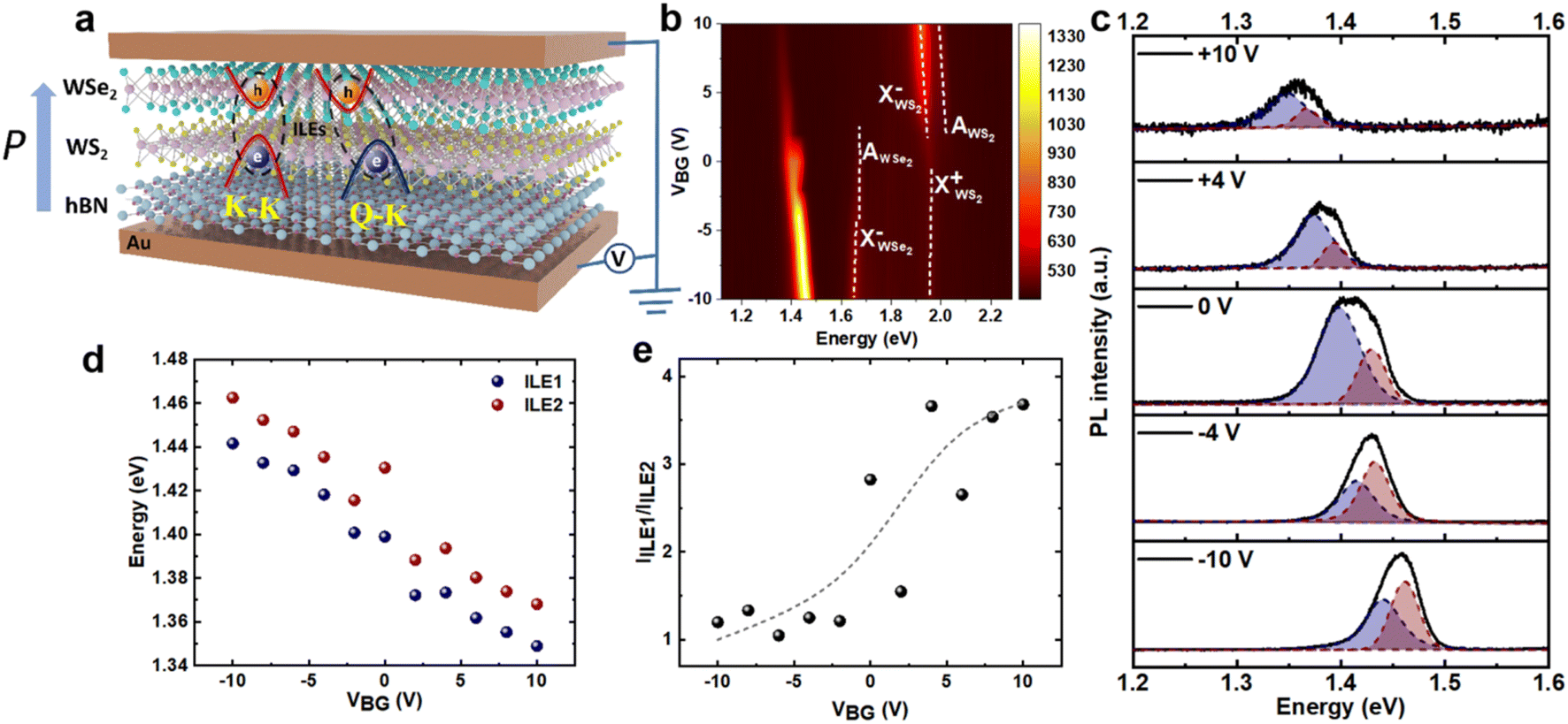 | ||
| Fig. 4 Gate-voltage-dependent PL measurement of the WSe2/WS2 heterostructure at 7 K. (a) The schematic of the setup used for the gate-voltage-dependent PL measurements. (b) The color plot of the PL intensity as a function of gate voltage. (c) PL spectra at the gate voltages of −10, −4, 0, +4, and +10 V. (d) The peak positions of ILE1 and ILE2 as functions of the gate voltage. (e) The ratio of the integrated peak intensities (IILE1/IILE2) as a function of gate voltage. | ||
The external electric field also strongly modified the emission of the interlayer exciton. Fig. 4c shows the PL spectrum at five specific gate voltages. Obviously, with the gate voltage increasing from −10 V to 10 V, both ILE1 and ILE2 showed significant red shifts. This phenomenon may be attributed to the interaction between the external electric field and the dipole of the interlayer exciton, which can be briefly described as ΔU = |P·EE|, where, P is the dipole (as shown in Fig. 4a), and E is the direction of the external electric field. When E is antiparallel (parallel) to the direction of dipole P, the energy of the interlayer exciton should blue shift (red shift). The variation of peak position versus gate voltage is shown in Fig. 4d, the ratios of the peak position and gate voltage were ∼4.9 meV V−1 (ILE1) and ∼5.0 meV V−1 (ILE2). Such similarity also confirms that the two interlayer emissions feature excitons rather than the interlayer trion because the variation of energy in the electric field would be different for interlayer trions and interlayer excitons due to the different types of charges carried by them, leading to differences in the dipole.49,50 The intensity of the interlayer exciton also changed with the gate voltage (as shown in Fig. 4b). Obviously, as the gate voltage was decreased from 10 V to −10 V, the intensity of the interlayer exciton was strongly enhanced. This phenomenon may be ascribed to the interaction between the interlayer exciton with the external electric field; when Vg < 0 V, the direction of the external electric field is the same as that of exciton recombination (electron transition from WS2 to WSe2), which strongly enhances the recombination of the interlayer exciton, and vice versa. However, when an external electric field is applied, the extraction and injection of electrons from the heterostructure due to the electrode may also lead to this phenomenon. In order to eliminate this possibility as much as possible, we used hBN to shield the influence of the electrode in the heterostructure (details shown in Fig. S5†); however, the interlayer exciton shows the same trend with the change in voltage, which further confirms that the enhancement of interlayer excitons results from the interaction between the interlayer excitons and the external electric field. Notably, in addition to the overall intensity change of the interlayer exciton, the relative intensity of ILE1 and ILE2 also changed with changes in the external electric field (as shown in Fig. 4c). Fig. 4e shows the variation of the ratio of the ILE1 and ILE2 intensities (IILE1/IILE2) with the gate voltage. It can be seen that with the gate voltage increasing from −10 V to 10 V, the intensities of ILE1 and ILE2 displayed an interesting reversal phenomenon, and the ratio IILE1/IILE2 increased.
In order to understand the behavior of the interlayer excitons, the band structure of the WSe2/WS2 heterostructures with twist angles of 0°, 27.8°, 38.2° and 60° (Their side-views and top-views are shown in Fig. S6.†) were calculated by using the density functional theory (DFT), as shown in Fig. 5, where the color-coding indicates the contribution of each layer. In particular, when the twist angle approached 0° and 60°, the conduction band showed two valleys at the K point and the Q point, respectively. The valence band maximum (VBMK) and conduction band minimum (CBMK) located at K and K′ are entirely contributed by WSe2 and WS2 respectively, but the CBMQ located at Q is contributed by both WS2 and WSe2. Notably, the energy difference between CBMK − VBMK and CBMQ − VBMK varied between the WSe2/WS2 heterostructures with twist angles of 0° and 60°, which is consistent with our experimental results that the energies of their interlayer excitons are different. To further understand this phenomenon, the differential charge densities were calculated (as shown in Fig. S7†). Obviously, charge transfer in the WSe2/WS2 heterostructures with twist angles of 0° and 60° were higher than that in the WSe2/WS2 heterostructure with the twist angle close to 30°, which is consistent with our findings from the experimental results that interlayer excitons are strongly enhanced when the twist angle is close to 0° or 60°.
 | ||
| Fig. 5 The DFT calculations of the WSe2/WS2 heterostructures with different twist angles. (a)–(d) Depict the band structures of the WSe2/WS2 heterostructure with twist angles of 0°, 27.8°, 38.2° and 60°, respectively. | ||
Further, considering spin–orbit coupling in the WSe2/WS2 heterostructure with a twist angle of 0°, Fig. 6a and b show the spin-resolved band structure. Obviously, CBMK demonstrated very small splitting, which would make the electron more likely to spin-flip and result in a smaller DoP for ILE1 (as shown in Fig. 3f). However, the CBMQ band is entirely contributed by the spin-down state, which leads to the higher DoP of ILE2. Meanwhile, the CBMK and CBMQ show opposite spin directions, which results in the opposite DoP of ILE1 and ILE2. These results also confirm the nature of the K–K (Q–K) transition of the ILE2 (ILE1). Furthermore, we also calculated the behavior of the band structure under an electric field. Fig. 6c shows the band structure under the electric fields of ±0.5, ±0.3, and 0 V Å−1. Similar to the experimental findings, the direction of the electric field was from the WS2 layer to the WSe2 layer. The conduction band showed an obvious shift with the variation of the electric field from −0.5 V Å−1 to 0.5 V Å−1. Both CBMK and CBMQ became closer to the valence band, and the energy differences between K and Q are summarized in Fig. 6d. This phenomenon is consistent with our experimental results, in which the ILEs show a significant red shift with the increase of the electric field. Meanwhile, with an increasing electric field, the energy difference between CBMK and CBMQ increased; this behavior supports the fact that the electrons in CBMQ tend to relax to CBMK and suppress the transition path of Q–K. This is also the reason for the increase in the ratio of ILE1/ILE2 with an increase in gate voltage in the experiments (as shown in Fig. 4e).
 | ||
| Fig. 6 DFT calculations of the WSe2/WS2 heterostructure with a twist angle of 0°. (a) The component-resolved band structure of the WSe2/WS2 heterostructure with a twist angle of 0°. (b) The spin-resolved band structure of the WSe2/WS2 heterostructure with a twist angle of 0°. (c) The band structure as a function of gate voltage. (d) The energy of CBMK–VBMK and CBMQ–VBMK as a function of gate voltage. | ||
4. Conclusions
In summary, we have studied the evolution of the interlayer excitons with the twist angle in TMDC heterostructures by combining PL measurements and DFT calculations. Two strong interlayer excitons were observed when the twist angles were near 0° and 60° due to the enhancement of interlayer coupling. Furthermore, two interlayer excitons were identified as the direct and indirect interlayer excitons based on the gate-, excitation-power-, and helicity-dependent PL measurements. Helicity-resolved PL shows that the two interlayer excitons hold opposite DoP. By comparing these results with the DFT calculations, we could assign two interlayer excitons to the direct transition of K–K and the indirect transition of Q–K, respectively. Finally, the emission properties of the interlayer excitons were further regulated by applying an electric field, and their emission energy and intensity show great adjustability under the influence of the electric field. Our results show great potential in the field of twist-angle optoelectronic-dependent devices in the future.Author contributions
Chunxiao Cong directed the research work. Chunxiao Cong, Jiajun Chen and Xiaofei Yue conceived and designed the experiments. Jiajun Chen fabricated the samples and implements the project. Jiajun Chen, Xiaofei Yue, Yabing Shan, Huishan Wang, Jinkun Han, conducted the experiments. Weihuang Yang perform the DFT calculations. Chunxiao Cong, Jiajun Chen, Xiaofei Yue, Weihuang Yang and Zhi-Jun Qiu analyzed the data. Chunxiao Cong and Jiajun Chen co-wrote the manuscript. All authors discussed the results and commented on the manuscript.Conflicts of interest
There are no conflicts to declare.Acknowledgements
This work is supported by the National Key R&D Program of China (Grant No. 2018YFA0703700, Grant No. 2017YFF0206106), the Shanghai Municipal Science and Technology Commission (Grant No. 20ZR1403200), the National Natural Science Foundation of China (Grant No. 61774040, 61774042), the Strategic Priority Research Program of Chinese Academy of Sciences (Grant No. XDB30000000), and the National Young 1000 Talent Plan of China.Notes and references
- D. Xiao, G. B. Liu, W. Feng, X. Xu and W. Yao, Phys. Rev. Lett., 2012, 108, 196802 CrossRef PubMed.
- H. Zeng, J. Dai, W. Yao, D. Xiao and X. Cui, Nat. Nanotechnol., 2012, 7, 490–493 CrossRef CAS PubMed.
- K. F. Mak, K. He, C. Lee, G. H. Lee, J. Hone, T. F. Heinz and J. Shan, Nat. Mater., 2013, 12, 207–211 CrossRef CAS PubMed.
- Y. Lin, X. Ling, L. Yu, S. Huang, A. L. Hsu, Y. H. Lee, J. Kong, M. S. Dresselhaus and T. Palacios, Nano Lett., 2014, 14, 5569–5576 CrossRef CAS PubMed.
- Y. You, X. X. Zhang, T. C. Berkelbach, M. S. Hybertsen, D. R. Reichman and T. F. Heinz, Nat. Phys., 2015, 11, 477–481 Search PubMed.
- J. X. Li, W. Q. Li, S.-H. Hung, P. L. Chen, Y. C. Yang, T. Y. Chang, P. W. Chiu, H. T. Jeng and C. H. Liu, Nat. Nanotechnol., 2022, 17, 721–728 CrossRef CAS PubMed.
- C. Gong, H. Zhang, W. Wang, L. Colombo, R. M. Wallace and K. Cho, Appl. Phys. Lett., 2013, 103, 053513 CrossRef.
- V. O. Özçelik, J. G. Azadani, C. Yang, S. J. Koester and T. Low, Phys. Rev. B, 2016, 94, 035125 CrossRef.
- H. M. Hill, A. F. Rigosi, K. T. Rim, G. W. Flynn and T. F. Heinz, Nano Lett., 2016, 16, 4831–4837 CrossRef CAS PubMed.
- N. R. Wilson, P. V. Nguyen, K. Seyler, P. Rivera, A. J. Marsden, Z. P. Laker, G. C. Constantinescu, V. Kandyba, A. Barinov and N. D. Hine, Sci. Adv., 2017, 3, e1601832 CrossRef PubMed.
- E. Barré, O. Karni, E. Liu, A. L. O'Beirne, X. Chen, H. B. Ribeiro, L. Yu, B. Kim, K. Watanabe, T. Taniguchi, K. Barmak, C. H. Lui, S. Refaely-Abramson, F. H. da Jornada and T. F. Heinz, Science, 2022, 376, 406–410 CrossRef PubMed.
- J. Peng, C. Ren, W. Zhang, H. Chen, X. Pan, H. Bai, F. Jing, H. Qiu, H. Liu and Z. Hu, ACS Nano, 2022, 16, 21600–21608 CrossRef CAS PubMed.
- C. Jin, J. Kim, M. I. B. Utama, E. C. Regan, H. Kleemann, H. Cai, Y. Shen, M. J. Shinner, A. Sengupta and K. Watanabe, Science, 2018, 360, 893–896 CrossRef CAS PubMed.
- P. Rivera, J. R. Schaibley, A. M. Jones, J. S. Ross, S. Wu, G. Aivazian, P. Klement, K. Seyler, G. Clark and N. J. Ghimire, Nat. Commun., 2015, 6, 1–6 Search PubMed.
- P. Rivera, K. L. Seyler, H. Yu, J. R. Schaibley, J. Yan, D. G. Mandrus, W. Yao and X. Xu, Science, 2016, 351, 688–691 CrossRef CAS PubMed.
- X. Zhu, N. R. Monahan, Z. Gong, H. Zhu, K. W. Williams and C. A. Nelson, J. Am. Chem. Soc., 2015, 137, 8313–8320 CrossRef CAS PubMed.
- Y. Yoon, Z. Zhang, R. Qi, A. Y. Joe, R. Sailus, K. Watanabe, T. Taniguchi, S. Tongay and F. Wang, Nano Lett., 2022, 22, 10140–10146 CrossRef CAS PubMed.
- J. E. Zimmermann, Y. D. Kim, J. C. Hone, U. Höfer and G. Mette, Nanoscale Horiz., 2020, 5, 1603–1609 RSC.
- L. Yuan, B. Zheng, J. Kunstmann, T. Brumme, A. B. Kuc, C. Ma, S. Deng, D. Blach, A. Pan and L. Huang, Nat. Mater., 2020, 19, 617–623 CrossRef CAS PubMed.
- C. Zhang, C. P. Chuu, X. Ren, M.-Y. Li, L. J. Li, C. Jin, M. Y. Chou and C. K. Shih, Sci. Adv., 2017, 3, e1601459 CrossRef PubMed.
- H. Yu, G. B. Liu, J. Tang, X. Xu and W. Yao, Sci. Adv., 2017, 3, e1701696 CrossRef PubMed.
- R. Xiong, J. H. Nie, S. L. Brantly, P. Hays, R. Sailus, K. Watanabe, T. Taniguchi, S. Tongay and C. Jin, Science, 2023, eadd5574 Search PubMed.
- H.-J. Chuang, M. Phillips, K. M. McCreary, D. Wickramaratne, M. R. Rosenberger, V. P. Oleshko, N. V. Proscia, M. Lohmann, D. J. O'Hara, P. D. Cunningham, C. S. Hellberg and B. T. Jonker, ACS Nano, 2022, 16, 16260–16270 CrossRef CAS PubMed.
- O. Karni, E. Barré, V. Pareek, J. D. Georgaras, M. K. L. Man, C. Sahoo, D. R. Bacon, X. Zhu, H. B. Ribeiro, A. L. O'Beirne, J. Hu, A. Al-Mahboob, M. M. M. Abdelrasoul, N. S. Chan, A. Karmakar, A. J. Winchester, B. Kim, K. Watanabe, T. Taniguchi, K. Barmak, J. Madéo, F. H. da Jornada, T. F. Heinz and K. M. Dani, Nature, 2022, 603, 247–252 CrossRef CAS PubMed.
- E. M. Alexeev, D. A. Ruiz-Tijerina, M. Danovich, M. J. Hamer, D. J. Terry, P. K. Nayak, S. Ahn, S. Pak, J. Lee and J. I. Sohn, Nature, 2019, 567, 81–86 CrossRef CAS PubMed.
- Z. Ji, H. Hong, J. Zhang, Q. Zhang, W. Huang, T. Cao, R. Qiao, C. Liu, J. Liang and C. Jin, ACS Nano, 2017, 11, 12020–12026 CrossRef CAS PubMed.
- P. K. Nayak, Y. Horbatenko, S. Ahn, G. Kim, J. U. Lee, K. Y. Ma, A.-R. Jang, H. Lim, D. Kim and S. Ryu, ACS Nano, 2017, 11, 4041–4050 CrossRef CAS PubMed.
- E. Calman, L. Fowler-Gerace, D. Choksy, L. Butov, D. Nikonov, I. Young, S. Hu, A. Mishchenko and A. Geim, Nano Lett., 2020, 20, 1869–1875 CrossRef CAS PubMed.
- H. Yu, G. B. Liu and W. Yao, 2D Mater., 2018, 5, 035021 CrossRef.
- M. Long, P. Wang, H. Fang and W. Hu, Adv. Funct. Mater., 2019, 29, 1803807 CrossRef.
- Y. Tang, K. F. Mak and J. Shan, Nat. Commun., 2019, 10, 1–7 CrossRef PubMed.
- Y. Zhou, G. Scuri, D. S. Wild, A. A. High, A. Dibos, L. A. Jauregui, C. Shu, K. De Greve, K. Pistunova and A. Y. Joe, Nat. Nanotechnol., 2017, 12, 856–860 CrossRef CAS PubMed.
- J. Chen, K. Shao, W. Yang, W. Tang, J. Zhou, Q. He, Y. Wu, C. Zhang, X. Li, X. Yang, Z. Wu and J. Kang, ACS Appl. Mater. Interfaces, 2019, 11, 19381–19387 CrossRef CAS PubMed.
- G. Cheng, B. Li, C. Zhao, X. Yan, H. Wang, K. M. Lau and J. Wang, Nano Lett., 2018, 18, 5640–5645 CrossRef CAS PubMed.
- K. Wang, B. Huang, M. Tian, F. Ceballos, M.-W. Lin, M. Mahjouri-Samani, A. Boulesbaa, A. A. Puretzky, C. M. Rouleau and M. Yoon, ACS Nano, 2016, 10, 6612–6622 CrossRef CAS PubMed.
- C. Jin, E. C. Regan, A. Yan, M. Iqbal Bakti Utama, D. Wang, S. Zhao, Y. Qin, S. Yang, Z. Zheng and S. Shi, Nature, 2019, 567, 76–80 CrossRef CAS PubMed.
- S. Zhang, H. M. Hill, K. Moudgil, C. A. Richter, A. R. Hight Walker, S. Barlow, S. R. Marder, C. A. Hacker and S. J. Pookpanratana, Adv. Mater., 2018, 30, 1802991 CrossRef PubMed.
- A. Chernikov, A. M. Van Der Zande, H. M. Hill, A. F. Rigosi, A. Velauthapillai, J. Hone and T. F. Heinz, Phys. Rev. Lett., 2015, 115, 126802 CrossRef PubMed.
- X. Lu, M. Utama, X. Wang, W. Xu, W. Zhao, M. H. S. Owen and Q. Xiong, Small, 2017, 13, 1701039 CrossRef PubMed.
- L. Wu, C. Cong, J. Shang, W. Yang, Y. Chen, J. Zhou, W. Ai, Y. Wang, S. Feng and H. Zhang, Nano Res., 2021, 14, 2215–2223 CrossRef CAS.
- S. Tongay, W. Fan, J. Kang, J. Park, U. Koldemir, J. Suh, D. S. Narang, K. Liu, J. Ji and J. Li, Nano Lett., 2014, 14, 3185–3190 CrossRef CAS PubMed.
- N. Peimyoo, J. Shang, W. Yang, Y. Wang, C. Cong and T. Yu, Nano Res., 2015, 8, 1210–1221 CrossRef CAS.
- J. T. Mlack, P. Masih Das, G. Danda, Y. C. Chou, C. H. Naylor, Z. Lin, N. P. López, T. Zhang, M. Terrones, A. T. C. Johnson and M. Drndić, Sci. Rep., 2017, 7, 43037 CrossRef CAS PubMed.
- M. Kremser, M. Brotons-Gisbert, J. Knörzer, J. Gückelhorn, M. Meyer, M. Barbone, A. V. Stier, B. D. Gerardot, K. Müller and J. J. Finley, npj 2D Mater. Appl., 2020, 4, 1–6 CrossRef.
- A. Branny, G. Wang, S. Kumar, C. Robert, B. Lassagne, X. Marie, B. D. Gerardot and B. Urbaszek, Appl. Phys. Lett., 2016, 108, 142101 CrossRef.
- B. Laikhtman and R. Rapaport, Phys. Rev. B: Condens. Matter Mater. Phys., 2009, 80, 195313 CrossRef.
- L. Butov, A. Shashkin, V. Dolgopolov, K. Campman and A. Gossard, Phys. Rev. B: Condens. Matter Mater. Phys., 1999, 60, 8753 CrossRef CAS.
- W. T. Hsu, L. S. Lu, D. Wang, J. K. Huang, M. Y. Li, T. R. Chang, Y. C. Chou, Z. Y. Juang, H. T. Jeng and L. J. Li, Nat. Commun., 2017, 8, 1–7 CrossRef CAS PubMed.
- J. Shang, X. Shen, C. Cong, N. Peimyoo, B. Cao, M. Eginligil and T. Yu, ACS Nano, 2015, 9, 647–655 CrossRef CAS PubMed.
- E. Liu, E. Barré, J. van Baren, M. Wilson, T. Taniguchi, K. Watanabe, Y. T. Cui, N. M. Gabor, T. F. Heinz, Y. C. Chang and C. H. Lui, Nature, 2021, 594, 46–50 CrossRef CAS PubMed.
Footnotes |
| † Electronic supplementary information (ESI) available. See DOI: https://doi.org/10.1039/d3ra02952b |
| ‡ These authors contributed equally to this work. |
| This journal is © The Royal Society of Chemistry 2023 |