
 Open Access Article
 This Open Access Article is licensed under a Creative Commons Attribution-Non Commercial 3.0 Unported Licence
Achieving above 24% efficiency with non-toxic CsSnI3 perovskite solar cells by harnessing the potential of the absorber and charge transport layers†
M. Khalid Hossain *a,
M. Shihab Uddinb,
G. F. Ishraque Tokic,
Mustafa K. A. Mohammedd,
Rahul Pandeye,
Jaya Madan*e,
Md. Ferdous Rahmanf,
Md. Rasidul Islamg,
Sagar Bhattaraih,
H. Bencherif*i,
D. P. Samajdarj,
Mongi Amamik and
D. K. Dwivedil
*a,
M. Shihab Uddinb,
G. F. Ishraque Tokic,
Mustafa K. A. Mohammedd,
Rahul Pandeye,
Jaya Madan*e,
Md. Ferdous Rahmanf,
Md. Rasidul Islamg,
Sagar Bhattaraih,
H. Bencherif*i,
D. P. Samajdarj,
Mongi Amamik and
D. K. Dwivedil
aInstitute of Electronics, Atomic Energy Research Establishment, Bangladesh Atomic Energy Commission, Dhaka 1349, Bangladesh. E-mail: khalid.baec@gmail.com; khalid@kyudai.jp
bDepartment of Electrical and Electronic Engineering, Islamic University, Kushtia 7000, Bangladesh
cCollege of Materials Science and Engineering, Donghua University, Shanghai 201620, China
dUniversity of Warith Al-Anbiyaa, 56001 Karbala, Iraq
eVLSI Centre of Excellence, Chitkara University Institute of Engineering and Technology, Chitkara University, Punjab 140401, India. E-mail: jaya.madan@chitkara.edu.in
fAdvanced Energy Materials and Solar Cell Research Laboratory, Department of Electrical and Electronic Engineering, Begum Rokeya University, Rangpur 5400, Bangladesh
gDepartment of Electrical and Electronic Engineering, Bangamata Sheikh Fojilatunnesa Mujib Science & Technology University, Jamalpur 2012, Bangladesh
hTechnology Innovation and Development Foundation, Indian Institute of Technology Guwahati, Guwahati 781039, Assam, India
iLEREESI, Higher National School of Renewable Energies, Environment and Sustainable Development, Batna 05078, Algeria. E-mail: bencherif.hichem@hns-re2sd.dz
jDept. of ECE, Indian Institute of Information Technology, Design & Manufacturing, Madhya Pradesh 482005, India
kDepartment of Chemistry, College of Sciences, King Khalid University, P.O. Box 9004, Abha, Saudi Arabia
lDepartment of Physics and Material Science, Madan Mohan Malaviya University of Technology, Gorakhpur, 273010, U.P., India
First published on 4th August 2023
Abstract
Lead toxicity is a barrier to the widespread commercial manufacture of lead halide perovskites and their use in solar photovoltaic (PV) devices. Eco-friendly lead-free perovskite solar cells (PSCs) have been developed using certain unique non- or low-toxic perovskite materials. In this context, Sn-based perovskites have been identified as promising substitutes for Pb-based perovskites due to their similar characteristics. However, Sn-based perovskites suffer from chemical instability, which affects their performance in PSCs. This study employs theoretical simulations to identify ways to improve the efficiency of Sn-based PSCs. The simulations were conducted using the SCAPS-1D software, and a lead-free, non-toxic, and inorganic perovskite absorber layer (PAL), i.e. CsSnI3 was used in the PSC design. The properties of the hole transport layer (HTL) and electron transport layer (ETL) were tuned to optimize the performance of the device. Apart from this, seven different combinations of HTLs were studied, and the best-performing combination was found to be ITO/PCBM/CsSnI3/CFTS/Se, which achieved a power conversion efficiency (PCE) of 24.73%, an open-circuit voltage (VOC) of 0.872 V, a short-circuit current density (JSC) of 33.99 mA cm−2 and a fill factor (FF) of 83.46%. The second highest PCE of 18.41% was achieved by the ITO/PCBM/CsSnI3/CuSCN/Se structure. In addition to optimizing the structure of the PSC, this study also analyzes the current density–voltage (J–V) along with quantum efficiency (QE), as well as the impact of series resistance, shunt resistance, and working temperature, on PV performance. The results demonstrate the potential of the optimized structure identified in this study to enhance the standard PCE of PSCs. Overall, this study provides important insights into the development of lead-free absorber materials and highlights the potential of using CsSnI3 as the PAL in PSCs. The optimized structure identified in this study can be used as a base for further research to improve the efficiency of Sn-based PSCs.
1 Introduction
To meet the huge energy crisis of the 21st century, the popularity of perovskite1,2 and thin-film solar cells has been channelized toward the efficient production of renewable solar energy, which has shown an exponential growth rate in the last few years. Among the various types of solar cells, perovskite solar cells (PSCs) have become predominant for their ideal tunable bandgaps, long diffusion length, better carrier transfer and ease of fabrication.3–9 It has also been noticed in recent studies that MAPbI3 is conventionally used in perovskite solar cells since its introduction in 2009 by Kojima et al.10 Extensive research also confirms that lead (Pb)-based PSCs have higher efficiencies than those based on Pb-free perovskites.11,12 Despite the advantage of efficiency, the toxicity of Pb and environmental issues are always a concern while using these perovskites. To overcome these problems, researchers have proposed Pb-free perovskites, which provide greater efficiency.13,14 A few metals, such as Sn, Ge, Bi, Sb, and Cu, can be utilized instead of Pb for the synthesis of metal hybrid perovskites. Over the past few years, tin (Sn)-based perovskites are used greatly amongst these metals because of their improved optical15 and electronic properties, such as higher charge mobility and narrow bandgaps.16–18 Meanwhile, the chemical instability of the crystal structure and the mismatch of energy levels between the absorber layer and charge transport layer are the main drawbacks of Sn-based perovskites that impede them from achieving higher efficiencies. Therefore, lead-free, non-volatile CsSnI3 can be used as the perovskite absorber material (PAL).However, at the moment, simple oxidation of Sn2+ is the fundamental issue that prevents the development of CsSnI3-based PSCs. The devices nonetheless operate poorly despite carrying out the whole manufacturing process in an inert environment because a trace amount of oxidation products already exists in the solution used as the precursor. B–CsSnI3 easily degrades in the ambient environment to form the yellow polymorph CsSnI3 and then Cs2SnI6, which contains tetravalent tin. Compared with B–CsSnI3, Cs2SnI6 has a significantly reduced light-harvesting capability.19 Consequently, the poor device stability, as well as low power conversion efficiency, of CsSnI3-based solar cells is caused by the unintended oxidation of Sn2+ to Sn4+, which significantly reduces their application potential in the photovoltaic field. The precursor state is where Sn2+ oxidation is about to take place, mostly in three ways. The first possibility is Sn2+ self-disproportionation, which results in Sn4+ and Sn0.20 The second is oxidation by dimethylsulfoxide (DMSO), a popular solvent for Sn-based perovskites.21 The third method is oxidation by the extremely little quantity of oxygen added to the precursor solution. According to a new report by Marshall et al., adding SnCl2 as an additive to perovskite photovoltaics (PPV) based on CsSnI3 results in higher efficiency, as well as improved device stability.22 Their findings might represent progress towards lead-free perovskite PPVs. For a CsSnI3 thin-film photovoltaic, Hatton and colleagues evaluated the effect of a number of tin halide additives, including SnF2, SnCl2, SnBr2, and SnI2, which showed encouraging results.22
CsSnI3 is a prototypical single halide perovskite with the formula of AMX3, where A denotes a monovalent inorganic/organic cation (such as Cs+, MA+, FA+), M denotes a divalent cation (such as Pb2+, Sn2+, Ge2+) and X denotes a halogen anion (such as I−, Br−, Cl−).23 Among the monovalent cations, Cs+ could provide better power conversion efficiency (PCE) because of its higher stability than MA+ and FA+ when used as a cation in the PSC.24–26 Chen et al. have reported that despite having a smaller bandgap of 1.3 eV, a PCE of 12.92% was achieved when CsSnI3 was used as the PAL.16–18 On the contrary, Song et al. found that the low efficiency for the absorber CsSnI3 was 3.83% in comparison to other reported studies.27 The absorber layer is placed in between the hole transport layer (HTL) and the electron transport layer (ETL) and helps in the transfer of holes and electrons in the entire device,28–32 whereas the ETL helps the extraction and transport of electrons33 in PSCs and eliminates electrical shunts between the transparent electrode and the perovskite layer. An ideal ETL should have high electron mobility and hole-blocking properties, which can also prevent potential reactions between the cathode and the perovskite layer.34 Among the many organic and inorganic ETL materials, phenyl-C61-butyric acid methyl ester (PCBM) has been utilized widely over the years due to the reduced number of film defects and, by extension, less unwanted electron–hole recombination between the perovskite layer and the electrode with the ETL. Since it is crucial to achieve a homogeneous and pin-hole-devoid PCBM layer, some attempts to enhance PCBM layers have been made by employing processing methods, such as refining the spin-coating rates and solvents. According to Bai et al., PCBM used as the ETL in the PSC device improved the efficiency up to 9.56%.35
On the other hand, the HTL generally aids in extracting and transporting the holes36 in the absorber layer to the electrode and functions as an energy barrier to prevent electron transport to the anode.37 In Sn-based PSCs, the energy levels of ITO and the PAL do not match, which results in decreased hole collection and photovoltaic (PV) outputs.38 Therefore, the HTL should match the energy level of the PAL and possess high hole mobility for transporting holes to the anode along with a low absorption coefficient.39 Similar to the ETL, some organic and inorganic HTLs, such as Spiro-MeOTAD, PEDOT:PSS, P3HT, NiO, CuI, CuSCN, and CFTS (Cu2FeSnS4), are frequently utilized in various solar cells.40–49 Amongst these HTLs, Spiro-MeOTAD and PEDOT:PSS are being used widely in most PSCs due to their high performance. However, among all these HTLs, CFTS provides the best efficiency probably due to the low energy level difference between CsSnI3 and CFTS.39
In our previous study,50 we evaluated the suitability of a variety of ETLs and HTLs from 70 different configurations to find the ideal combination for the CsSnI3 absorber layer-based PSC to achieve good PV performance. In this study, CsSnI3 is used as the lead-free PAL to bring out the best configurations from the previous study50 and optimize various parameters toward increasing the device efficiency, for the very first time, by combining the PCBM ETL with various HTLs, including Spiro-MeOTAD, PEDOT:PSS, P3HT, NiO, CuI, CuSCN, and CFTS, via SCAPS-1D (one-dimensional solar cell capacitance simulator) software. Because of the time and effort required to investigate all these materials, getting the best possible result from scientific experiments can be difficult. Only a few theoretical and experimental studies have been done on CsSnI3-based PSCs, offering many opportunities to improve their performance. Here, the maximum efficiency of the non-toxic Sn-based CsSnI3 PSC is targeted by varying different features, including the back metal contact, PAL, ETL, and HTL, using the SCAPS-1D simulation software. Additionally, the influence of series resistance, shunt resistance, and working temperature on the PV performance of the PSC have been investigated besides the current density–voltage and quantum efficiency (QE) parameters. Finally, the resulting highly efficient devices are contrasted against earlier experiments in terms of their capacity to improve the typical PCE.
2 Materials and methodology
2.1 SCAPS-1D numerical simulation
The SCAPS-1D software was introduced by Professor M. Burgelman at the University of Gent and has been used to simulate different solar cell configurations.51–59 The SCAPS-1D simulator uses fundamental semiconductor equations, in terms of the Poisson equations (eqn 1), and continuity equations for excitons (electrons and holes).60,61
 | (1) |
The continuity equation for an electron is represented below (eqn (2)),
 | (2) |
The continuity equation for holes is given by eqn (3),
 | (3) |
The drift and diffusion equations are given by eqn (4) and (5), respectively,
 | (4) |
 | (5) |
2.2 The CsSnI3-based perovskite solar cell structure
The structure consisted of ITO, which was used as the transparent conductive oxide (TCO), the ETL, PAL, HTL, and lastly a back metal contact. The PAL was sandwiched between the ETL and the HTL. The ETL helps in extracting, collecting and transferring electrons, and HTL works on blocking electrons and collecting holes from the PAL and transferring these holes to the cathode. The structure of our solar cell was ITO/ETL/CsSnI3/HTL/Se. Fig. 1 shows the configuration of the CsSnI3-based solar cell used in this simulation. | ||
| Fig. 1 Configuration of CsSnI3 solar cells used in this numerical simulation. | ||
Here, initially, the PCBM ETL was combined with different HTLs (CuSCN, NiO, P3HT, PEDOT:PSS, Spiro-MeOTAD, Cul, and CFTS) along with a fixed PAL (CsSnI3) and back metal contact (Au). After that, the back metal contact (like Au, W, Ni, Pd, Pt, Se, Ag, C, Fe, and Cu) was varied to obtain the optimum structure among the seven studied structures. Then, the input parameters, such as the thickness of PAL, ETL, and HTL, the collective impact of PAL and HTL acceptor and defect density, the ETL donor and defect density, and interface defects were further optimized stepwise, and the optimized outcomes were added progressively with the other optimized parameters in this study. The study was carried out at the illumination of AM1.5 and the solar irradiation intensity of 100 mW cm−2. In Tables 1 and 2, the input parameters utilized in the simulation are summarized. While Table 1 represents the values of the different parameters of ITO, the ETL (PCBM), the PAL (CsSnI3), and different HTLs, Table 2 represents the values of the interface defects.
| Parameters | ITO | CuSCN | PCBM | P3HT | PEDOT:PSS | Spiro-MeOTAD | NiO | CuI | CFTS | CsSnI3 |
|---|---|---|---|---|---|---|---|---|---|---|
| a In this study, these values remained constant during initial optimization to get the best combination of HTL, ETL, and Back metal contact. | ||||||||||
| Thickness (nm) | 500 | 50 | 50 | 50 | 50 | 200 | 100 | 100 | 100 | 800a |
| Eg (eV) | 3.5 | 3.6 | 2 | 1.7 | 1.6 | 3 | 3.8 | 3.1 | 1.3 | 1.3 |
| X (eV) | 4 | 1.7 | 3.9 | 3.5 | 3.4 | 2.2 | 1.46 | 2.1 | 3.3 | 3.6 |
| εr | 9 | 10 | 3.9 | 3 | 3 | 3 | 10.7 | 6.5 | 9 | 9.93 |
| NC (cm−3) | 2.2 × 10¹⁸ | 2.2 × 10¹⁹ | 2.5 × 10²¹ | 2 × 10²¹ | 2.2 × 10¹⁸ | 2.2 × 10¹⁸ | 2.8 × 10¹⁹ | 2.8 × 10¹⁹ | 2.2 × 10¹⁸ | 1 × 10¹⁹ |
| Nv (cm−3) | 1.8 × 10¹⁹ | 1.8 × 10¹⁸ | 2.5 × 10²¹ | 2 × 10²¹ | 1.8 × 10¹⁹ | 1.8 × 10¹⁹ | 1 × 10¹⁹ | 1 × 10¹⁹ | 1.8 × 10¹⁹ | 1 × 10¹⁸ |
| μn (cm2 V−1 s−1) | 20 | 100 | 0.2 | 1.8 × 10⁻³ | 4.5 × 10⁻² | 2.1 × 10⁻³ | 12 | 100 | 21.98 | 1.5 × 10³ |
| μh (cm2 V−1 s−1) | 10 | 25 | 0.2 | 1.86 × 10⁻² | 4.5 × 10⁻² | 2.16 × 10⁻³ | 2.8 | 43.9 | 21.98 | 5.85 × 10² |
| NA (cm−3) | 0 | 1 × 10¹⁸ | 0 | 1 × 10¹⁸ | 1 × 10¹⁸ | 1.0 × 10¹⁸ | 1 × 10¹⁸ | 1.0 × 10¹⁸ | 1 × 10¹⁸ | 1020 |
| ND (cm−3) | 1 × 10²¹ | 0 | 2.93 × 10¹⁷ | 0 | 0 | 0 | 0 | 0 | 0 | 0 |
| Nt (cm−3) | 1 × 10¹⁵a | 1 × 10¹⁵a | 1 × 10¹⁵a | 1 × 10¹⁵a | 1 × 10¹⁵a | 1.0 × 10¹⁵a | 1 × 10¹⁵a | 1.0 × 10¹⁵a | 1 × 10¹⁵a | 1 × 10¹⁵a |
| Interface | Defect type | Capture cross section: electrons/holes (cm2) | Energetic distribution | Reference for defect energy level | Total density (cm−2) (integrated overall energies) |
|---|---|---|---|---|---|
| ETL/CsSnI3 | Neutral | 1.0 × 10⁻¹⁷ | Single | Above the VB maximum | 1.0 × 10¹⁰ |
| 1.0 × 10⁻¹⁸ | |||||
| CsSnI3/HTL | Neutral | 1.0 × 10⁻¹⁸ | Single | Above the VB maximum | 1.0 × 10¹⁰ |
| 1.0 × 10⁻¹⁹ |
3 Result and discussion
3.1 The influence of CsSnI3 thickness and the acceptor doping density on PV performance
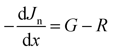
Research on PSCs has seen tremendous progress in recent years, achieving higher efficiency and potential for low-cost production. However, to further enhance the performance and stability of PSCs, it is essential to examine the impact of various parameters on device performance. Two such parameters are absorber thickness and acceptor doping density, which are critical to optimizing the efficiency of PSCs. The absorber thickness in PSCs plays a substantial role in determining the efficiency of the device. The optimal thickness of the absorber layer is determined by the bandgap and absorption coefficient of the material, which dictate the amount of light that can be absorbed by the device. A thick absorber layer may increase the photon absorption rate, but it can also lead to an increased recombination rate, which would reduce the efficiency of the device. Conversely, a thinner absorber layer may reduce the photon absorption rate but can also reduce the recombination rate and improve device efficiency. Acceptor doping density is another critical parameter that affects the performance of PSCs. Doping acceptor atoms into the absorber layer can modify the band structure and improve the carrier transport properties of the device. However, excessive doping can lead to increased defects and reduced carrier lifetimes, which negatively impact the device efficiency. Therefore, optimization of the acceptor doping density is crucial to achieving high device efficiency.A combined study of absorber thickness and acceptor doping density is essential for optimizing the performance of PSCs. By optimizing both parameters simultaneously, it is possible to achieve the highest possible device efficiency. The absorber thickness must be optimized to balance the photon absorption and recombination rates, while the acceptor doping density must be carefully controlled to minimize the influence of defects on device performance. Therefore, a collective study of the effects of absorber thickness and acceptor doping density was carried out. Fig. 2–5 illustrate the changes in the PV characteristics, namely VOC, JSC, FF, and PCE, of the solar cell with the variation of the absorber layer acceptor density and thickness; while the absorber layer was varied from 100 nm to 1300 nm, the acceptor density (NA) was varied from 1 × 109 cm−3 to 1.0 × 1021 cm−3.
 | ||
| Fig. 2 (a)–(g) Contour graphs of the dependency of the VOC of PSCs with different HTLs on the thickness and acceptor density of the absorber. | ||
 | ||
| Fig. 3 (a)–(g) Contour graphs of the dependency of the JSC of PSCs with different HTLs on the thickness and acceptor density of the absorber. | ||
 | ||
| Fig. 4 (a)–(g) Contour graphs of the dependency of the FF of PSC with different HTLs on the acceptor density and thickness of the absorber. | ||
 | ||
| Fig. 5 (a)–(g) Contour graphs of the dependency of the PCE of PSCs with different HTLs on the thickness and acceptor density of the absorber. | ||
The dependency of the VOC of the ITO/PCBM/CsSnI3/CFTS/Se device is shown in Fig. 2(a). Here, the highest VOC of 0.927 V was achieved at a thickness <800 nm and NA > 8 × 1020 cm−3 and started declining before and after 800 nm thickness. The lowest value of VOC i.e. 0.827 V was recorded at thickness >1000 nm. From Fig. 2(b), while using CuI as the HTL, the highest VOC of >0.914 V was achieved at thickness <200 nm and NA of >1.0 × 1021 cm−3. With the increase in thickness to >200 nm and decrease in NA to <8.0 × 1020 cm−3, the value of VOC dropped from 0.889 V to 0.826 V.
Similarly, Fig. 2(c) and (e)–(g) demonstrate that the VOC of these configurations varied from 0.826 V to 0.927 V in the presence of other tested HTLs except NiO. The highest VOC of >0.914 V was achieved at thickness <200 nm and NA >1.0 × 1021 cm−3. With the increase in thickness to >200 nm and a decrease in NA to <8.0 × 1020 cm−3, the values of VOC dropped from 0.889 V to 0.826 V. On the contrary, while using NiO as the HTL, the VOC varied from 0.839 V to 0.927 V, as seen in Fig. 2(d), while the highest VOC of >0.914 V was achieved at absorber thickness <600 nm and NA < 8.0 × 1020 cm−3. With the increase in thickness to values >800 nm and decrease in NA below 8.0 × 1020 cm−3, the value of VOC dropped from 0.894 V to 0.839 V (Fig. 2(d)).
The dependency of JSC of the device ITO/PCBM/CsSnI3/CFTS/Se is shown in Fig. 3(a). From the figure, it is evident that JSC varied from 6.20 mA cm−2 to 34.10 mA cm−2. The highest JSC values > 30.61 mA cm−2 were achieved at thicknesses <800 nm, and they were independent of NA. At higher NA < 8.0 × 1020 cm−3, the value of JSC dropped from 20.15 mA cm−2 to 6.20 mA cm−2. Similarly, Fig. 3(b) demonstrates the JSC variation of the device with CuI as the HTL from 6.20 mA cm−2 to 34.30 mA cm−2. At thickness >400 nm and NA < 8.0 ×1020 cm−3, JSC increased from 27.28 mA cm−2 to 34.30 mA cm−2. At higher NA < 8.0 × 1020 cm−3, the value of JSC dropped from 20.25 mA cm−2 to 6.2 mA cm−2. Similarly, Fig. 3(c), (e) and (f) illustrate that JSC varied from 6.20 mA cm−2 to 34.30 mA cm−2 in the presence of other HTLs except NiO. At thickness >400 nm and NA < 8.0 × 1020 cm−3, JSC increased from 27.28 mA cm−2 to 34.30 mA cm−2. At higher NA < 8.0 × 1020 cm−3, the value of JSC dropped from 20.25 mA cm−2 to 6.20 mA cm−2.
On the other hand, from Fig. 3(d), it can be seen that JSC varied from 6.20 mA cm−2 to 34 mA cm−2 when NiO was employed as the HTL. At thickness >800 nm, JSC gradually decreased from 16.63 mA cm−2 to 6.20 mA cm−2. At thicknesses higher than 800 nm, the value of JSC increased from 20.10 mA cm−2 to 34.00 mA cm−2. The dependency of JSC of the device ITO/PCBM/CsSnI3/Spiro-MeOTAD/Se is shown in Fig. 3(g); in this case, JSC varied from 6.20 mA cm−2 to 34.20 mA cm−2. At thickness >400 nm and NA < 8.0 × 1020 cm−3, JSC increased from 27.20 mA cm−2 to 34.20 mA cm−2. At higher NA < 8.0 × 1020 cm−3, the value of JSC dropped from 23.70 mA cm−2 to 6.20 mA cm−2.
The dependency of the FF for the device with the ITO/PCBM/CsSnI3/CFTS/Se structure is shown in Fig. 4(a), and FF varied from 74.58% to 80.90%. At thickness <400 nm and NA < 6.0 × 1020 cm−3, the device showed maximum FF values >80.11%, and with the increase in thickness and NA, it gradually decreased from 78.53% to 74.58%. Fig. 4(b) demonstrates that FF varied from 73.60% to 82.60% while using CuI as the HTL; at thickness >300 nm and NA < 6.0 × 1020 cm−3, the FF of the device increased from 80.35% to 82.60% but with further increase in thickness to >1000 nm, the FF tended to decline. At thickness <200 nm and NA > 6.0 × 1020 cm−3, respectively, the FF decreased from 80.35% to 73.60%. Similarly, from Fig. 4(e) and (f), it can be seen that FF varied from 73.70% to 82.60% for P3HT (Fig. 4(e)) and 73.88% to 82.60% for PEDOT:PSS (Fig. 4(f)). Meanwhile at thickness >300 nm and NA < 6.0 × 1020 cm−3, the FF of the devices increased from 80.88% to 82.60%, but a further increase in thickness to >1000 nm led to a decline in FF. Moreover, at thickness and <200 nm and NA > 6.0 × 1020 cm−3, respectively, the FF decreased up to 73.70% and 73.88% (Fig. 4(e) and (f)).
In contrast, Fig. 4(c), illustrates that FF varied from 73.60% to 82.50% when the CuSCN HTL was employed. At thickness >300 nm and NA < 6.0 × 1020 cm−3, the FF of the device increased from 80.28% to 82.50%. However, a further increase in thickness to >1000 nm caused an FF decline. At thickness <200 nm and NA > 6.0 × 1020 cm−3, respectively, the FF decreased from 80.28% to 73.60%. From Fig. 4(d), it can be seen that the FF varied from 74.58% to 82.60% with the NiO HTL. In particular, at thickness <800 nm, the FF of the device decreased from 79.59% to 74.58%, but a further increase in thickness to >900 nm causes the FF to rise in the range of 2.0 × 1020 cm−3 to 8.0 × 1020 cm−3. Further, the FF values of the ITO/PCBM/CsSnI3/Spiro-MeOTAD/Se device varied from 72.90% to 80.40%; at thickness >200 nm and NA < 6.0 × 1020 cm−3, its FF increased from 78.52% to 80.40%, but a further increase in thickness to >900 nm caused FF to decline. At thickness <200 nm and NA > 6.0 × 1020 cm−3 respectively, FF decreased to 72.90% (Fig. 4(g)).
The dependency of the PCE of the ITO/PCBM/CsSnI3/CFTS/Se device is shown in Fig. 5(a). From the figure, it can be seen that its PCE varied from 4.3% to 23.50%. At thickness >200 nm and NA < 6.0 × 1020 cm−3, the PCE of the device increased from 18.70% to 23.50%, and with the decrease in thickness and increase in NA, the PCE gradually decreased from 18.70% to 4.30%. A similar trend of PCE was seen in the other devices except for that using the Spiro-MeOTAD HTL, as shown in Fig. 5(b)–(f). For all these devices, PCE varied from 4.3% to 23.80%. At thickness >200 nm and NA of < 8.0 × 1020 cm−3, the PCE of the devices increases from 18.92% to 23.80%. At lower thicknesses <200 nm and NA of < 8.5 × 1020 cm−3, the PCE values decreased from 16.49% to 11.61%, and with a further increase in the value of NA, the PCE dropped to 4.3% independent of thickness variation. Moreover, the PCE for the device of ITO/PCBM/CsSnI3/Spiro-MeOTAD/Se is shown in Fig. 5(g), which was the lowest among all the structures. It was noticed that its PCE varied from 4.35% to 23.30%. At thickness >200 nm and NA < 8.0 × 1020 cm−3, the PCE of this device increased from 18.56% to 23.30%. At lower thicknesses <200 nm and NA of < 8.5 × 1020 cm−3, the PCE decreased from 16.19% to 11.46%, but with a further increase in the value of NA, the PCE dropped to 4.35% independent of the thickness variation.
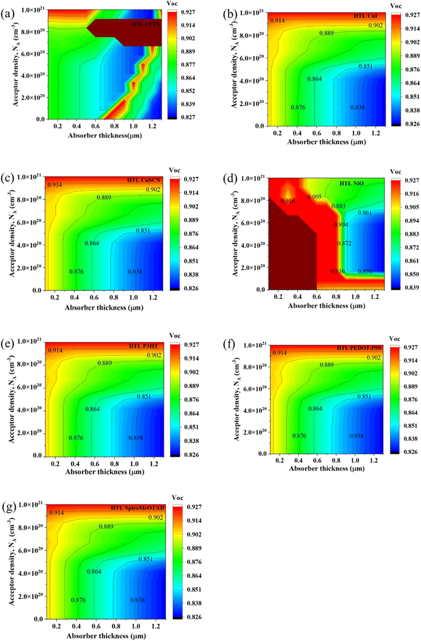
3.2 The influence of CsSnI3 thickness and defect density
Defect density is another essential parameter that affects the performance of PSCs. Defects in the absorber layer act as recombination centers, thereby reducing the carrier lifetime and efficiency of the device. Therefore, controlling the defect density of the absorber layer is crucial to achieving high device efficiency. The influence of CsSnI3 absorber thickness and defect density on PSC performance has been extensively studied, and it has been shown that the two parameters are interrelated. By optimizing both parameters simultaneously, it is possible to achieve the highest possible device efficiency. The optimal CsSnI3 thickness and defect density depend on the specific material and device architecture. Fig. 6–9 illustrate the changes in PV characteristics, including VOC, JSC, FF, and PCE, of the solar cell with the variation of absorber layer defect density (Nt) and thickness. The thickness of the absorber layer was varied from 100 nm to 1300 nm, and Nt was varied from 1.0 × 109 cm−3 to 1.0 × 1021 cm−3. The dependency of VOC of the ITO/PCBM/CsSnI3/CFTS/Se device was the lowest of all structures, as shown in Fig. 6(a). From the graph, it can be seen that its VOC varied from 0.845 V to 0.909 V. Though it seems like its VOC is almost independent of the thickness of the absorber, at Nt > 8.0 × 1020 cm−3, VOC gradually decreased from 0.909 V to 0.845 V. The dependency of VOC for the rest of the studied devices ITO/PCBM/CsSnI3/HTL/Se is shown in Fig. 6(b)–(f). From the graphs, it can be seen that their VOC varied from 0.845 V to 0.916 V. The VOC values seemed to be almost independent of the thickness of the absorber. However, at defect density >8.0 × 1020 cm−3, VOC gradually decreased from 0.916 V to 0.845 V.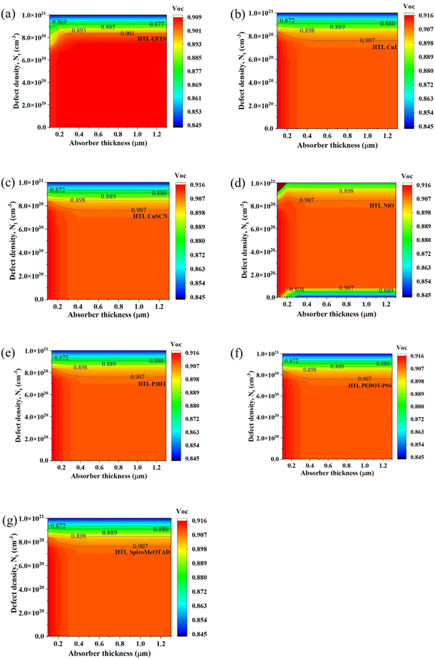 | ||
| Fig. 6 (a)–(g) Contour graphs of the dependency of the VOC of PSCs with different HTLs on the defect density and thickness of the PAL. | ||
 | ||
| Fig. 7 (a)–(g) Contour graphs of the dependency of the JSC of PSCs with different HTLs on the defect density and thickness of the PAL. | ||
 | ||
| Fig. 8 (a)–(g) Contour graphs of the dependency of the FF of PSCs with different HTLs on the defect density and thickness of the PAL. | ||
 | ||
| Fig. 9 (a)–(g) Contour graphs of the dependency of the PCE of PSCs with different HTLs on the defect density and thickness of the PAL. | ||
The dependency of JSC of the ITO/PCBM/CsSnI3/CFTS/Se device was the least among all the tested devices, as depicted in Fig. 7(a). From the graph, it can be seen that its JSC varied from 4.15 mA cm−2 to 14.20 mA cm−2. Although it seems like its JSC is almost independent of the thickness of the absorber, at Nt > 7.5 × 1020 cm−3, JSC gradually decreased from 14.20 mA cm−2 to 4.15 mA cm−2. On the other hand, the dependency of the JSC of the rest of the studied devices ITO/PCBM/CsSnI3/HTL/Se was higher, as shown in Fig. 7(b)–(f). From the graphs, it can be seen that JSC varied from 4.15 mA cm−2 to 14.80 mA cm−2. Their JSC values seemed to be almost independent of the thickness of the absorber. However, at Nt > 8.0 × 1020 cm−3, JSC gradually decreased from 12.14 mA cm−2 to 4.15 mA cm−2. At lower Nt, all the studied devices displayed better JSC.
The dependency of FF of the ITO/PCBM/CsSnI3/CFTS/Se device was the lowest of all, as shown in Fig. 8(a). From the graph, it can be seen that FF varied from 68.00% to 78.10%. It seems like its FF is almost independent of the thickness of the absorber. However, at Nt > 8.0 × 1020 cm−3, FF gradually decreased from 78.10% to 68.00%. On the contrary, the dependency of FF for the rest of the studied devices ITO/PCBM/CsSnI3/HTL/Se was higher, as shown in Fig. 8(b)–(f). From the graphs, it can be seen that their FF varied from 68.00% to 78.70%. Their FF values seemed to be almost independent of the thickness of the absorber. However, at Nt > 8.0 × 1020 cm−3, FF gradually decreased from 78.70% to 68.00%.
The dependency of PCE of the ITO/PCBM/CsSnI3/CFTS/Se device is shown in Fig. 9(a). From the graph, it can be seen that PCE varied from 2.40% to 10.10%. It seems like its PCE is almost independent of the thickness of the absorber. However, at Nt > 8.0 × 1020 cm−3, PCE gradually decreased from 10.10% to 2.40%. On the contrary, the dependency of PCE for the rest of the studied devices ITO/PCBM/CsSnI3/HTL/Se was higher, as presented in Fig. 9(b)–(f). For all the structures, it is evident that the PCE varied from 2.40% to 10.62%. It seemed like their PCE values were almost independent of the thickness of the absorber. However, at Nt > 8.0 × 1020 cm−3, PCE gradually decreased from 10.62% to 2.40%.
3.3 The influence of the back metal work function
The choice of back metal contact (BMC) plays a crucial role in the performance of PSCs. In this regard, a detailed investigation was carried out to determine the impact of different BMCs on the efficiency of the PSC. Initially, different metals were used as the back metal contact (BMC) in the simulation to optimize the performance of the structures. Table 3 depicts the work functions (WFs) of the different BMCs used in the optimization study. From this study, it was seen that the efficiency of the different back contacts increased with the increase in the WF of the structure. This is because the Schottky barrier vanishes when the WF is increased to the Fermi level of the studied HTL.62 The lowest efficiency was achieved for silver (Ag) as the back contact because it presented a lower metal WF than others. On the contrary, almost all BMCs, including when carbon (C), nickel (Ni), tungsten (W), gold (Au), platinum (Pt), and palladium (Pd), resulted in improved PV features (Table S1 in the ESI†). Based on the availability, higher WF, and performance, selenium (Se) was chosen as the optimum BMC, and the ITO/PCBM/CsSnI3/HTL/Se configuration was used for further optimization of PAL, ETL, and HTL in this study.| Back metal contacts | Cu | Ag | Fe | C | Au | W | Ni | Pd | Pt | Se |
|---|---|---|---|---|---|---|---|---|---|---|
| Work function (eV) | 4.65 | 4.26 | 4.81 | 5 | 5.1 | 5.22 | 5.5 | 5.6 | 5.7 | 5.9 |
3.4 Optimization of PAL, ETL, and HTL thickness
The optimization of the thickness of the PAL, ETL, and HTL is critical for achieving high efficiency in PSCs. The thickness of these layers can significantly affect the absorption and collection of light, charge transport, and recombination, which ultimately determine the device performance. In this section, we present the results of the optimization of PAL, ETL, and HTL thickness aimed at achieving maximum device efficiency.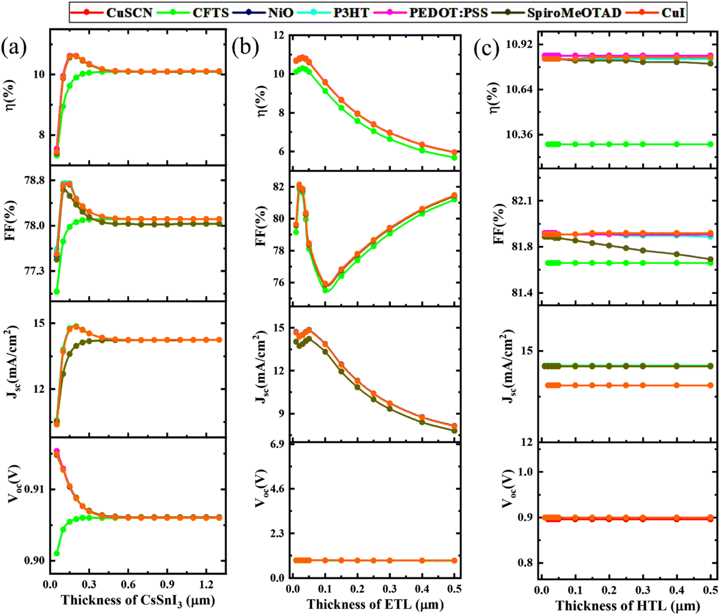 | ||
| Fig. 10 The impact of variations in the (a) thickness of PAL, (b) thickness of ETL, and (c) thickness of HTL on the performance parameters of the PSCs. | ||
For the ITO/PCBM/CsSnI3/CuSCN/Se device, when the PAL thickness was increased, VOC dropped from 0.918 V to 0.909 V. Moreover, JSC increased initially from 10.39 mA cm−2 to 14.84 mA cm−2 and then decreased slightly to 14.24 mA cm−2. Identically, with increasing PAL thickness, FF first increased from 77.50% to 78.68% and then decreased to 78.11%, and PCE also increased from 7.39% to 10.61% and further declined to 10.11%. Similarly, the devices ITO/PCBM/CsSnI3/NiO/Se, ITO/PCBM/CsSnI3/P3HT/Se, ITO/PCBM/CsSnI3/PEDOT:PSS/Se, ITO/PCBM/CsSnI3/Spiro-MeOTAD/Se, ITO/PCBM/CsSnI3/CuI/Se also presented similar trends of PV parameters with an increase in PAL thickness. Because the highest efficiency was obtained at 200 nm, we considered this as the optimum thickness for the simulated PSC structures.
On the other hand, for the device ITO/PCBM/CsSnI3/CFTS/Se, as PAL thickness increased, VOC, JSC, and FF increased from 0.903 V to 0.909 V, 10.53 mA cm−2 to 14.24 mA cm−2, and 76.91% to 78.11%, respectively. Although the PCE of the device also increased initially from 7.32% to 10.11%, it stabilized at 10.11% with a further increase in absorber layer thickness. Since the maximum efficiency was observed at 1000 nm, it was taken as the optimum thickness for the next steps of optimization. The increment of all these parameters happens due to the increase in the photon capturing ability with the CsSnI3 absorber thickness,63 and then, the values tend to decrease with a further increment in absorber layer thickness. At a certain point, they almost stabilize at a fixed value because of the increase in recombination charge carrier and pathway resistance. For the optimum efficiency of the device, the absorber thickness should match the diffusion length of the charge carrier. After the simulation, based on the PCE, the optimum thickness of the absorber layer was taken as 1000 nm when CFTS is used as HTL and for other HTLs, the value was 200 nm.
3.5 Optimization of the PAL properties
 | ||
| Fig. 11 (a) The influence of changes in the acceptor density in the absorber on the performance parameters, and (b) the influence of the defect density in the absorber on the performance parameters. | ||
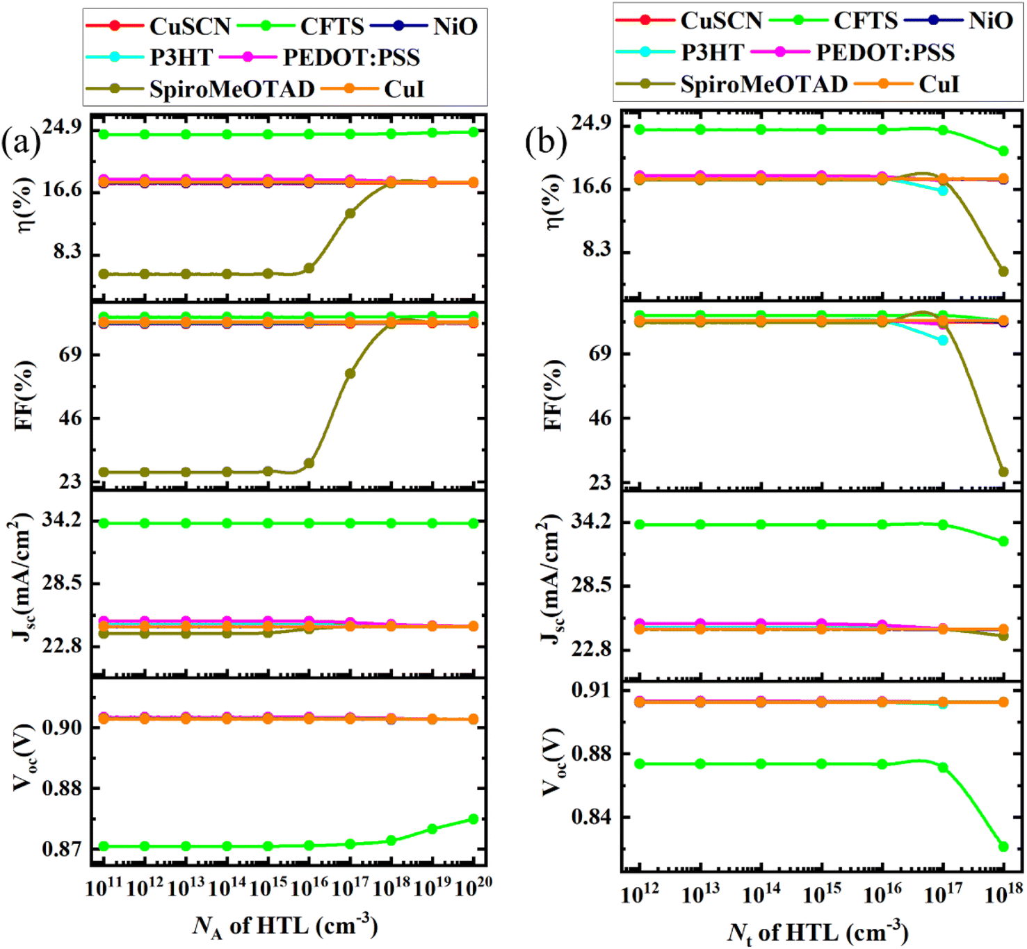
For the ITO/PCBM/CsSnI3/CuSCN/Se device, with increasing NA in the PAL, VOC increased from 0.898 V to 0.955 V, JSC increased from 24.33 mA cm−2 to 24.70 mA cm−2 and then dropped to 2.53 mA cm−2 with a further increase NA, FF increased initially from 80.87% to 82.29% and then dropped to 81.04%, and PCE also increased from 17.68% to 17.79% and later dropped to 1.96%. The ITO/PCBM/CsSnI3/P3HT/Se, ITO/PCBM/CsSnI3/PEDOT:PSS/Se, ITO/PCBM/CsSnI3/Spiro-MeOTAD/Se, ITO/PCBM/CsSnI3/CuI/Se, and ITO/PCBM/CsSnI3/CFTS/Se structures also showed a similar trend in performance. Considering the highest efficiency, the optimum NA in the absorber layer was decided as 1018 cm−3 for all HTLs except the CFTS HTL. On the contrary, while increasing the NA of the absorber, the ITO/PCBM/CsSnI3/NiO/Se structure showed an increase in VOC from 0.903 V to 0.927 V and a decrease in JSC from 24.63 mA cm−2 to 5.56 mA cm−2, while FF increases from 79.97% to 82.3% and then dropped to 81.93%, and PCE decreased from 17.8% to 4.22%. Considering the maximum efficiency, the optimum NA of the absorber layer is determined as 1018 cm−3 while NiO is used as HTL.
VOC increased with the increase in NA because when NA increases, the Fermi energy level drops, which results in a VOC rise.67 In the case of most HTLs, PV features like JSC, FF, and PCE tended to increase gradually till 1018 cm−3, and then, the values dropped. Because more electric field is generated with the increase in NA, it also causes the recombination of charge carriers. While CFTS was used as the HTL, the optimum value of 1017 cm−3 was considered, for which the best improvement in efficiency from 10.30% to 24.28% was achieved. For all the other HTLs, the optimum value of NA was 1018 cm−3. However, CFTS provided the best efficiency because of the better band alignment between the HOMOs of CFTS and CsSnI3.43
For the ITO/PCBM/CsSnI3/CuSCN/Se device, with the increase in absorber layer Nt, VOC decreased from 0.904 V to 0.764 V, JSC decreased from 24.63 mA cm−2 to 12.16 mA cm−2, FF decreased from 79.95% to 63.52% and PCE also decreased from 17.79% to 5.9%. The ITO/PCBM/CsSnI3/NiO/Se, ITO/PCBM/CsSnI3/P3HT/Se, ITO/PCBM/CsSnI3/PEDOT:PSS/Se, ITO/PCBM/CsSnI3/Spiro-MeOTAD/Se, ITO/PCBM/CsSnI3/CuI/Se, and ITO/PCBM/CsSnI3/CFTS/Se structures displayed a similar kind of decline in PV performance with the increase in absorber layer Nt. The optimum absorber layer Nt was taken as 1015 cm−3 for all the structures except the case of CFTS as the HTL, for which an Nt of 1013 cm−3 was considered.
The values of VOC, JSC, FF, and PCE remained constant till an Nt of 1013 cm−3 when CFTS was used as the HTL, and for all other HTLs, they were constant till the Nt value of 1015 cm−3 and decreased with a further increase in absorber layer Nt, which is similar to the previous studies.68 Therefore, these values are taken as the best optimum absorber layer Nt. The reason behind this decline in PV parameters at higher absorber layer Nt is carrier recombination, which leads to lifetime reduction and thereby reduced device performance.63 The maximum efficiency was achieved at a lower defect density as well, but we could not consider it as the optimum value as it is nearly impossible to experimentally synthesize a material with such a small Nt.67
3.6 Optimization of the ETL properties
 | ||
| Fig. 12 (a) The influence of changes in the donor density in the ETL on the performance parameters, and (b) the influence of changes in the defect density in the ETL on the performance parameters. | ||
In the simulation of the device structure ITO/PCBM/CsSnI3/CuSCN/Se, while on increasing the ND value of the ETL, VOC increased from 0.903 V to 0.911 V, JSC decreased from 24.63 mA cm−2 to 22.82 mA cm−2, FF increased from 80.79% to 87.01% and PCE increased from 17.98% to 18.09%. The ITO/PCBM/CsSnI3/NiO/Se, ITO/PCBM/CsSnI3/P3HT/Se, ITO/PCBM/CsSnI3/PEDOT:PSS/Se, ITO/PCBM/CsSnI3/Spiro-MeOTAD/Se, ITO/PCBM/CsSnI3/CuI/Se, and ITO/PCBM/CsSnI3/CFTS/Se devices also showed an increase in VOC, FF, and PCE, while JSC declined for all the combinations. Based on the results, the optimum ND of ETL PCBM was taken as 1017, 1015, 1014, 1015, 1015, 1015, and 1018 cm−3, which resulted in the maximum performance of the respective structures.
The VOC, FF, and PCE increase with the increase in ND of the ETL because at higher donor density, more charge extraction and transportation occur at the ETL/perovskite interfaces, and at lower values of ND, these parameters are low because of series resistance.69,70 The JSC tended to decrease after a certain value of donor density of the ETL. Therefore, we chose the value of ND as close as possible to the reference work given in Table 1 with better efficiency.
For the device of ITO/PCBM/CsSnI3/CuSCN/Se, while increasing the defect density of the ETL, VOC decreased slightly, JSC decreased from 24.64 mA cm−2 to 24.56 mA cm−2, FF decreased from 80.47% to 78.98% and PCE decreased from 17.91% to 17.52%. Similarly, the ITO/PCBM/CsSnI3/NiO/Se, ITO/PCBM/CsSnI3/P3HT/Se, ITO/PCBM/CsSnI3/PEDOT:PSS/Se, ITO/PCBM/CsSnI3/Spiro-MeOTAD/Se, ITO/PCBM/CsSnI3/CuI/Se, and ITO/PCBM/CsSnI3/CFTS/Se devices tended to decline in PV performance. The optimum Nt for the ETL for the respective devices were 1014, 1014, 1015, 1014, 1014, 1014 and 1015 cm−3, accordingly. It can be seen that there was not much change in the electrical parameters with the variation of the ETL layer defect density. However, the VOC, JSC, FF, and PCE values tended to decrease after the value of defect density reached 1015 cm−3. This is maybe because of the recombination of charge carriers.63 For CFTS and P3HT, the maximum values of ETL defect density remained at the initial values, while for the other HTLs used, the value of 1014 cm−3 was considered it is closer to their initial values.
3.7 Optimization of the HTL properties
 | ||
| Fig. 13 (a) The influence of changes in the acceptor density in the HTL on the performance parameters, and (b) the influence of changes in the defect density in the HTL on the performance parameters. | ||
For the device of ITO/PCBM/CsSnI3/CuSCN/Se, while increasing the value of the NA of CuSCN, VOC decreased from 0.9035 V to 0.9034 V, JSC increased from 24.644 mA cm−2 to 24.638 mA cm−2, FF increased from 80.18% to 80.49%, and PCE increased from 17.85% to 17.92%. The performance of the ITO/PCBM/CsSnI3/NiO/Se, ITO/PCBM/CsSnI3/Spiro-MeOTAD/Se, and ITO/PCBM/CsSnI3/CFTS/Se structures was very similar to this. The optimum NA for the CuSCN, NiO, Spiro-MeOTAD, and CFTS HTLs was taken as 1018 cm−3. On the other hand, for the ITO/PCBM/CsSnI3/P3HT/Se structure, while increasing the value of the NA of P3HT, VOC decreased from 0.904 V to 0.903 V, JSC decreased from 24.80 mA cm−2 to 24.63 mA cm−2, FF increased from 80.65% to 80.81%, and PCE decreased from 18.07% to 17.98%. Moreover, the performance of ITO/PCBM/CsSnI3/PEDOT:PSS/Se also showed the same trend with increasing NA. The optimum NA values for P3HT and PEDOT:PSS were taken as 1016 and 1015 cm−3, respectively. For the device ITO/PCBM/CsSnI3/CuI/Se, while increasing NA of CuI, VOC and FF remained unchanged in this range, while JSC decreased marginally, and PCE decreased from 18% to 17.99%. The optimum NA for the CuI HTL was taken as 1018 cm−3, the same as the initial value.
Here, it seems like the change in HTL NA did not affect the performance parameters much. However, for all the HTLs except CFTS, the value of VOC decreased with the increase in NA of the HTL, and for CFTS, the value increased from 0.868 to 0.876 V. This increment may be due to the electric potential at the HTL/perovskite interface.71 In contrast, JSC, FF, and PCE increased with the increase in NA of the HTL because, at higher acceptor concentrations in the HTL, the conductivity increases and thus helps in collecting the charges faster due to enhanced electric field.72 For P3HT and PEDOT:PSS, the optimum NA was considered as 1016 cm−3 and 1015 cm−3, respectively, as their performance parameters declined after these values, and for the rest of the HTLs, the optimum NA remained the same as the initial value.
For the device of ITO/PCBM/CsSnI3/CuSCN/Se, while increasing the Nt of CuSCN, VOC increased from 0.903 V to 0.904 V, JSC decreased very slightly, while FF decreased from 80.47% to 80.18% and PCE decreased from 17.91% to 17.85%. The ITO/PCBM/CsSnI3/NiO/Se and ITO/PCBM/CsSnI3/CFTS/Se structures performed similarly. The optimum Nt for the CuSCN, NiO, and CFTS HTLs was taken as 1015 cm−3, which is the same as the initial value. On the contrary, for the ITO/PCBM/CsSnI3/P3HT/Se and ITO/PCBM/CsSnI3/PEDOT:PSS/Se structures, while increasing the Nt of P3HT and PEDOT:PSS, VOC decreased from 0.904 V to 0.903 V (almost unchanged), while JSC, FF, and PCE decreased as well like the other structures. The optimum Nt for P3HT and PEDOT:PSS was taken as 1014 cm−3, which is almost the same as the initial value.
However, for the ITO/PCBM/CsSnI3/Spiro-MeOTAD/Se device, while increasing the Nt of Spiro-MeOTAD, VOC remained unchanged in this range, and JSC, FF, and PCE decreased similar to the other studied structures. Meanwhile, for the ITO/PCBM/CsSnI3/CuI/Se device, while increasing the Nt of CuI, all the PV features like VOC, JSC, FF, and PCE remained unchanged within this range. The optimum Nt for Spiro-MeOTAD and CuI was taken as 1015 cm−3, which is the same as the initial value.
The values of the PV features remain unchanged until a certain value of Nt of the HTL, and then they begin to drop with a further increment in Nt. This decline is because of carrier recombination at higher defect densities.63 The maximum PCE was obtained at lower Nt too, but as it is nearly impossible to synthesize a material with very low Nt, we chose the close value of 1015 cm−3 as the optimum Nt, and it is the same as the initial value from Table 1.
3.8 Optimization of the interface properties
The band energy alignment of the interface energy levels of the charge transport layers and absorber material represents one of the issues that the PSC community is concerned about. To get overcome these challenges, attempts should be made to link experimental and theoretical studies. We could observe the formation of two distinct formations connected to the CBO of the ETL/CsSnI3 interface by the theoretical modeling described in Section 2, which hinges on the distinction between the electron affinities of the ETL (EAETL) and the absorber (EAAbsorber). In the scenario of PCBM, the energy cliff CBO– is generated with no possible barrier for electrons, which aids in the collection mechanism, if the conduction band of the ETL is less than that of the absorber. The spike-like conformation CBO+ is produced and acts as an electron barrier, if the conduction band of the ETL is substantially high in comparison with that of the perovskite. At the perovskite/HTL interface, an optimal energy band alignment is also necessary for enhanced PSC efficiency. The valence band of the absorber layer and that of HTM differ significantly. Valence energy alignment is necessary, as already mentioned, to improve the photovoltaic characteristics. The energy diagram of the perovskite active layer, HTLs, and ETL is shown in Fig. 14. This figure remarks the suitability of CFTS, which offers a suitable band alignment that enhances the collection mechanism and establishes an efficient blocking barrier for electrons. | ||
| Fig. 14 The energy diagram of the perovskite active layer and the charge transport materials. | ||
 | ||
| Fig. 15 (a) The effect of changes in the HTL/CsSnI3 interface defect density, Nt, on the performance parameters, and (b) the effect of changes in the CsSnI3/PCBM interface defect density, Nt, on the performance parameters. | ||
3.9 The influence of series resistance, shunt resistance, and temperature
 | ||
| Fig. 16 The influence of changes in (a) series resistance, RS (Ω cm2), (b) shunt resistance, RSh (Ω cm2), and (c) temperature (K) on the performance parameters VOC, JSC, FF, and PCE of PSCs. | ||
As seen in the figure, the values of VOC and JSC of all studied structures were not influenced much by the change in series resistance but the values of FF and efficiency gradually decreased with the increase in RS. Because, whenever series resistance increases, it causes a lack of power in the solar cell, thus declining the PCE of the solar cell.
The values of the performance parameters decreased with the increase in RSh because when the shunt resistance increases, the defect states decrease, leading to a reduction in the charge recombination rate, which increases the PCE of the solar cell.73,74 Therefore, it is obvious that a low value of RS and a high value of RSh are required to get a higher PCE. For an ideal solar device, the value of RS is zero, and the value of shunt resistance is infinite, but in practice, it is impossible to implement these values.
Here, the VOC of all structures tended to decrease with the increase in temperature because at higher temperatures, the reverse saturation current density (J0) increases. Due to the reverse relationship between VOC and J0, VOC decreases with the increase in J0, and this is represented in eqn (6).
 | (6) |
 is the thermal voltage.
From the simulation, it could be seen that temperature had almost no influence on JSC, but FF and PCE decreased with the increase in temperature. This decline may be due to the cutback of shunt resistance.75 Another possible reason for this decrement in PCE might be the enhanced charged recombination rate at higher temperatures due to the drop in charge recombination resistance.
3.10 The influence of current–voltage density and quantum efficiency
 | ||
| Fig. 17 (a) The current density–voltage curve for the initial optimized structure, (b) the current density–voltage curve for the final optimized structure ITO/PCBM/CsSnI3/HTL/Se, (c) the QE curve of the initial optimized structure and (d) the QE curve of the final optimized structure ITO/PCBM/CsSnI3/HTL/Se. | ||
3.11 Comparison of the SCAPS-1D results with previous work
The optimized results of the absorber layer, ETL layer, and HTL layer for the best-optimized device are listed in Table 4. Meanwhile, Table 5 represents the PV parameters from previous works (theoretical and practical studies) using CsSnI3 as the absorber layer for comparison with this work. From the table, it can be seen that CsSnI3 as an absorber layer couldn't provide the expected efficiency, but in the case of our optimized device, it provides greater efficiency compared with other works. Song et al. mixed piperazine with CsSnI3 to increase its PCE but was only able to achieve an efficiency of 3.83%.27 Chen et al. tried to replace the halide of CsSnI3 to get a better PCE but only got a PCE of 12.96%.16 Kumar et al. tried to mix SnF2 with an absorber layer and got only 2.02% efficiency for the device.76 Rahman et al. and Wang et al. experimentally obtained 11.41%77 and 3.31% PCE,78 respectively. With the optimized values from this study and our previous study,50 we found that the PCE of our device increased from 10.11% to 24.73%, and for a Pb-free PSC, this PCE value is remarkable as this solar cell is environmentally friendly due to its inorganic charge transport layers. Regarding fabrication feasibility, most of the sandwiched architecture-based perovskite solar cells reported in the literature are fabricated using spin-coating techniques, and the same can be utilised to fabricate the optimised ITO/PCBM/CsSnI3/CuSCN/Se-based solar cell. The thickness of each layer, material quality, annealing temperature, and encapsulation are important parameters to be considered when fabricating the device by spin-coating. With careful control of these parameters, it is possible to fabricate high-performance ITO/PCBM/CsSnI3/CuSCN/Se devices. Besides, the optimized CsSnI3 can be fabricated via different commonly used fabrication techniques, such as the doctor blade process, sequential deposition, hybrid chemical vapor, and alternating layer-by-layer process.79| Parameters | CFTS | CsSnI3 | PCBM |
|---|---|---|---|
| Thickness (nm) | 100 | 1000 | 30 |
| Eg (eV) | 1.3 | 1.3 | 2 |
| χ (eV) | 3.3 | 3.6 | 3.9 |
| εr | 9 | 9.93 | 3.9 |
| NC (cm−3) | 2.2 × 10¹⁸ | 1 × 10¹⁹ | 2.5 × 10²¹ |
| NV (cm−3) | 1.8 × 10¹⁹ | 1 × 10¹⁸ | 2.5 × 10²¹ |
| μn (cm2 V−1 s−1) | 21.98 | 1.5 × 10³ | 0.2 |
| μh (cm2 V−1 s−1) | 21.98 | 5.85 × 10² | 0.2 |
| NA (cm−3) | 1 × 10¹⁸ | 1 × 10²⁰ | — |
| ND (cm−3) | — | — | 2.93 × 10¹⁷ |
| Nt (cm−3) | 1.0 × 10¹⁵ | 1.0 × 10¹³ | 1.0 × 10¹⁵ |
| Type | Device structure | VOC (V) | JSC (mA cm−2) | FF (%) | PCE (%) | Ref. |
|---|---|---|---|---|---|---|
| a Note: 1- experimental, 2- theoretical.b This work. | ||||||
| 1 | FTO/TiO2/CsSnI3/Au | 0.34 | 20.63 | 54.18 | 3.83 | 27 |
| 1 | ITO/TiO2/CsSnI3/Spiro-OMeTAD/Au | 0.86 | 23.20 | 65.00 | 12.96 | 16 |
| 1 | FTO/TiO2/CsSnI3/m-MTDATA/Au | 0.24 | 22.70 | 0.37 | 2.02 | 76 |
| 2 | ITO/NiOx/CsSnI3/PCBM/Al | 1.19 | 17.29 | 55.27 | 11.41 | 77 |
| 2 | ITO/TiO2/MASnI3/Spiro-OMeTAD/Au | 0.88 | 16.80 | 0.42 | 6.40 | 80 |
| 2 | ITO/PCBM/CsSnI3/NiO2/Al | 0.52 | 10.21 | 62.50 | 3.31 | 78 |
| 2 | ITO/PCBM/CsSnI3/CuI/Au | 0.91 | 14.24 | 78.11 | 10.10 | 50 |
| 2 | ITO/PCBM/CsSnI3/CFTS/Se | 0.87 | 33.99 | 83.46 | 24.73 | b |
4 Conclusion
In this study, we conducted simulations for the optimization of the performance of lead-free CsSnI3-based solar cells with various HTLs and PCBM as the ETL. Our findings demonstrate that the optimal structure is ITO/PCBM/CsSnI3/CFTS/Se, which is capable of achieving a PCE of 24.73%, along with a VOC of 0.87 V, a JSC of 33.99 mA cm−2, and a FF of 83.46%. We also explored the influence of both series and shunt resistances on the PCE of the solar cells. Our results suggest that a smaller value of series resistance and a higher value of shunt resistance are suitable for achieving maximum efficiency. Additionally, we observed that the temperature significantly affects the PCE of the PSC, with the highest efficiency being achieved at 300 K. Furthermore, our study also reveals that the QE of solar cells is highly dependent on the choice of HTL. While using CFTS as the HTL, the QE curve showed a higher value of 99.6% in the visible range of 620 nm–650 nm. Overall, our simulations provide valuable insights into the optimization of CsSnI3-based solar cells with various HTLs and PCBM ETL. These findings can potentially contribute to developing cost-effective solar cells with higher efficiency for future applications.Data availability
The raw/processed data required to reproduce these findings cannot be shared at this time as the data also forms part of an ongoing study.Author contributions
M. K. Hossain: conceptualization, data curation, formal analysis, funding acquisition, investigation, methodology, project administration, resources, software, supervision, validation, visualization, writing – original draft, and writing – review & editing; M. S. Uddin, G. F. I. Toki, M. K. A. Mohammed, and R. Pandey: data curation, formal analysis, investigation, software, validation, visualization, and writing – original draft; J. Madan, M. F. Rahman, M. R. Islam, S. Bhattarai, H. Bencherif, D. P. Samajdar, Mongi Amami, and D. K. Dwivedi: data curation, formal analysis, investigation, validation, visualization, and writing – review & editing.Conflicts of interest
The authors declare that they have no known competing financial interests or personal relationships that could have appeared to influence the work reported in this paper.Acknowledgements
The authors have extend their appreciation to the Deanship of Scientific Research at King Khalid University, Saudi Arabia for funding this work through Research Groups Program under grant number R.G.P.2:200/44. The SCAPS-1D program was kindly provided by Dr M. Burgelman of the University of Gent in Belgium. The authors would like to express their gratitude to him.References
- M. H. K. Rubel, M. A. Hossain, M. K. Hossain, K. M. Hossain, A. A. Khatun, M. M. Rahaman, M. Ferdous Rahman, M. M. Hossain and J. Hossain, Results Phys., 2022, 42, 105977 CrossRef
.
- M. R. Islam, A. A. M. Mazumder, M. R. H. Mojumder, A. S. M. Z. Shifat and M. K. Hossain, Jpn. J. Appl. Phys., 2023, 62, 011002 CrossRef
- M. K. Hossain, M. H. K. Rubel, G. F. I. Toki, I. Alam, M. F. Rahman and H. Bencherif, ACS Omega, 2022, 7, 43210–43230 CrossRef CAS PubMed
- R. Pandey, S. Bhattarai, K. Sharma, J. Madan, A. K. Al-Mousoi, M. K. A. Mohammed and M. K. Hossain, ACS Appl. Electron. Mater., 2023 DOI:10.1021/acsaelm.2c01574
- H. Bencherif and M. K. Hossain, Sol. Energy, 2022, 248, 137–148 CrossRef CAS
- S. Kazim, M. K. Nazeeruddin, M. Grätzel and S. Ahmad, Angew. Chem., Int. Ed., 2014, 53, 2812–2824 CrossRef CAS PubMed
- M. K. Hossain, A. A. Arnab, R. C. Das, K. M. Hossain, M. H. K. Rubel, M. F. Rahman, H. Bencherif, M. E. Emetere, M. K. A. Mohammed and R. Pandey, RSC Adv., 2022, 12, 34850–34873 RSC
- A. K. Al-Mousoi, M. K. A. Mohammed, A. Kumar, R. Pandey, J. Madan, D. Dastan, M. K. Hossain, P. Sakthivel, A. Ganesan and Z. M. Yaseen, Phys. Chem. Chem. Phys., 2023, 25, 16459–16468 RSC
- M. H. K. Rubel, S. K. Mitro, M. K. Hossain, K. M. Hossain, M. M. Rahaman, J. Hossain, B. K. Mondal, A. Akter, M. F. Rahman, I. Ahmed and A. K. M. A. Islam, Mater. Today Commun., 2022, 33, 104302 CrossRef CAS
- A. Kojima, K. Teshima, Y. Shirai and T. Miyasaka, J. Am. Chem. Soc., 2009, 131, 6050–6051 CrossRef CAS PubMed
- L. Serrano-Lujan, N. Espinosa, T. T. Larsen-Olsen, J. Abad, A. Urbina and F. C. Krebs, Adv. Energy Mater., 2015, 5, 1501119 CrossRef
- S. Shao, J. Liu, G. Portale, H.-H. Fang, G. R. Blake, G. H. ten Brink, L. J. A. Koster and M. A. Loi, Adv. Energy Mater., 2018, 8, 1702019 CrossRef
- J. Wei, Q. Xiong, S. M. Mahpeykar and X. Wang, Nanomaterials, 2016, 6, 55 CrossRef PubMed
- F. Hao, C. C. Stoumpos, D. H. Cao, R. P. H. Chang and M. G. Kanatzidis, Nat. Photonics, 2014, 8, 489–494 CrossRef CAS
- S. Saurabh, M. K. Hossain, S. Singh, S. K. Agnihotri and D. P. Samajdar, RSC Adv., 2023, 13, 9878–9891 RSC
- L.-J. Chen, C.-R. Lee, Y.-J. Chuang, Z.-H. Wu and C. Chen, J. Phys. Chem. Lett., 2016, 7, 5028–5035 CrossRef CAS PubMed
- K. Shum, Z. Chen, J. Qureshi, C. Yu, J. J. Wang, W. Pfenninger, N. Vockic, J. Midgley and J. T. Kenney, Appl. Phys. Lett., 2010, 96, 221903 CrossRef
- Z. Chen, C. Yu, K. Shum, J. J. Wang, W. Pfenninger, N. Vockic, J. Midgley and J. T. Kenney, J. Lumin., 2012, 132, 345–349 CrossRef CAS
- X. Meng, J. Lin, X. Liu, X. He, Y. Wang, T. Noda, T. Wu, X. Yang and L. Han, Adv. Mater., 2019, 31, 1903721 CrossRef CAS PubMed
- Z. Zhu, N. Li, D. Zhao, L. Wang and A. K. -Y. Jen, Adv. Energy Mater., 2019, 9, 1802774 CrossRef
- Z. Zhang, Q. Sun, T. Nakajima, H. Ban, Z. Liu, H. Yu, Y. Wang, Z. Xiao, Y. Shen and M. Wang, J. Mater. Chem. A, 2022, 10, 23204–23211 RSC
- K. P. Marshall, M. Walker, R. I. Walton and R. A. Hatton, Nat. Energy, 2016, 1, 16178 CrossRef CAS
- K. Xu, Instrum. Sci. Technol., 2021, 49, 91–105 CrossRef CAS
- M. K. Hossain, M. K. A. Mohammed, R. Pandey, A. A. Arnab, M. H. K. Rubel, K. M. Hossain, M. H. Ali, M. F. Rahman, H. Bencherif, J. Madan, M. R. Islam, D. P. Samajdar and S. Bhattarai, Energy Fuels, 2023, 37, 6078–6098 CrossRef CAS
- M. K. Hossain, G. F. I. Toki, A. Kuddus, M. H. K. Rubel, M. M. Hossain, H. Bencherif, M. F. Rahman, M. R. Islam and M. Mushtaq, Sci. Rep., 2023, 13, 2521 CrossRef CAS PubMed
- B. Wu, Y. Zhou, G. Xing, Q. Xu, H. F. Garces, A. Solanki, T. W. Goh, N. P. Padture and T. C. Sum, Adv. Funct. Mater., 2017, 27, 1604818 CrossRef
- T. Bin Song, T. Yokoyama, J. Logsdon, M. R. Wasielewski, S. Aramaki and M. G. Kanatzidis, ACS Appl. Energy Mater., 2018, 1, 4221–4226 CrossRef
- D. Dastan, M. K. A. Mohammed, A. K. Al-Mousoi, A. Kumar, S. Q. Salih, P. S. JosephNg, D. S. Ahmed, R. Pandey, Z. M. Yaseen and M. K. Hossain, Sci. Rep., 2023, 13, 9076 CrossRef CAS PubMed
- M. K. Basher, S. M. Shah Riyadh, M. K. Hossain, M. Hassan, M. A. R. Akand, S. M. Amir-Al Zumahi, M. A. Matin, N. Das and M. Nur-E-Alam, Opt. Quantum Electron., 2023, 55, 322 CrossRef CAS
- M. K. A. Mohammed, A. K. Al-Mousoi, A. Kumar, A. R. J. Katae, O. A. Khaleel, D. S. Ahmed and M. K. Hossain, J. Mater. Sci., 2023, 58, 11748–11760 CrossRef CAS
- A. Thakur, D. Singh and S. Kaur Gill, Mater. Today: Proc., 2022, 71, 195–201 CrossRef CAS
- T. Dureja, A. Garg, S. Bhalla, D. Bhutani and A. Khanna, Mater. Today: Proc., 2022, 71, 239–242 CrossRef CAS
- Y. Miyamoto, S. Kusumoto, T. Yokoyama, Y. Nishitani, T. Matsui, T. Kouzaki, R. Nishikubo, A. Saeki and Y. Kaneko, ACS Appl. Nano Mater., 2020, 3, 11650–11657 CrossRef CAS
- N. Shrivastav, S. Kashyap, J. Madan, M. K. A. Mohammed, M. K. Hossain and R. Pandey, Optik, 2023, 281, 170821 CrossRef CAS
- Y. Bai, H. Yu, Z. Zhu, K. Jiang, T. Zhang, N. Zhao, S. Yang and H. Yan, J. Mater. Chem. A, 2015, 3, 9098–9102 RSC
- Z. Zhang, M. Sheri, Z. A. Page, T. Emrick, A. Saeki, Y. Liu and T. P. Russell, ACS Appl. Mater. Interfaces, 2020, 12, 56068–56075 CrossRef CAS PubMed
- S. Li, Y.-L. Cao, W.-H. Li and Z.-S. Bo, Rare Met., 2021, 40, 2712–2729 CrossRef CAS
- W. Liao, D. Zhao, Y. Yu, C. R. Grice, C. Wang, A. J. Cimaroli, P. Schulz, W. Meng, K. Zhu, R. Xiong and Y. Yan, Adv. Mater., 2016, 28, 9333–9340 CrossRef CAS PubMed
- L. Xu, X. Feng, W. Jia, W. Lv, A. Mei, Y. Zhou, Q. Zhang, R. Chen and W. Huang, Energy Environ. Sci., 2021, 14, 4292–4317 RSC
- M. K. Hossain, G. F. Ishraque Toki, D. P. Samajdar, M. H. K. Rubel, M. Mushtaq, M. R. Islam, M. F. Rahman, S. Bhattarai, H. Bencherif, M. K. A. Mohammed, R. Pandey and J. Madan, Energy Fuels, 2023, 37, 7380–7400 CrossRef CAS
- N. Shrivastav, S. Kashyap, J. Madan, A. K. Al-Mousoi, M. K. A. Mohammed, M. K. Hossain, R. Pandey and J. Ramanujam, Energy Fuels, 2023, 37, 3083–3090 CrossRef CAS
- H. Bencherif, F. Meddour, M. H. Elshorbagy, M. K. Hossain, A. Cuadrado, M. A. Abdi, T. Bendib, S. Kouda and J. Alda, Micro Nanostruct., 2022, 171, 207403 CrossRef CAS
- Y. Raoui, H. Ez-Zahraouy, N. Tahiri, O. El Bounagui, S. Ahmad and S. Kazim, Sol. Energy, 2019, 193, 948–955 CrossRef CAS
- N. Touafek, R. Mahamdi and C. Dridi, Dig. J. Nanomater. Biostructures, 2021, 16, 705–712 CrossRef
- L. Moulaoui, O. Bajjou, A. Najim, M. Archi and K. Rahmani, in 2022 2nd International Conference on Innovative Research in Applied Science, Engineering and Technology (IRASET), IEEE, 2022, pp. 1–7 Search PubMed
- M. M. Khatun, A. Sunny and S. R. Al Ahmed, Sol. Energy, 2021, 224, 956–965 CrossRef CAS
- Y. H. Khattak, F. Baig, H. Toura, S. Beg and B. M. Soucase, J. Electron. Mater., 2019, 48, 5723–5733 CrossRef CAS
- M. K. Hossain, G. F. I. Toki, J. Madan, R. Pandey, H. Bencherif, M. K. A. Mohammed, M. R. Islam, M. H. K. Rubel, M. F. Rahman, S. Bhattarai and D. P. Samajdar, New J. Chem., 2023, 47, 8602–8624 RSC
- S. Kashyap, J. Madan, M. K. A. Mohammed, M. K. Hossain, S. Ponnusamy and R. Pandey, Mater. Lett., 2023, 339, 134096 CrossRef CAS
- M. K. Hossain, G. F. I. Toki, D. P. Samajdar, M. Mushtaq, M. H. K. Rubel, R. Pandey, J. Madan, M. K. A. Mohammed, M. R. Islam, M. F. Rahman and H. Bencherif, ACS Omega, 2023, 8, 22466–22485 CrossRef CAS PubMed
- M. F. Rahman, N. Mahmud, I. Alam, M. H. Ali, M. M. A. Moon, A. Kuddus, G. F. I. Toki, M. H. K. Rubel, M. A. Al Asad and M. K. Hossain, AIP Adv., 2023, 13, 045309 CrossRef CAS
- A. Isha, A. Kowsar, A. Kuddus, M. K. Hossain, M. H. Ali, M. D. Haque and M. F. Rahman, Heliyon, 2023, 9, e15716 CrossRef CAS PubMed
- M. E. Islam, M. R. Islam, S. Ahmmed, M. K. Hossain and M. F. Rahman, Phys. Scr., 2023, 98, 065501 CrossRef
- M. K. A. Mohammed, A. K. Al-Mousoi, S. Singh, A. Kumar, M. K. Hossain, S. Q. Salih, P. Sasikumar, R. Pandey, A. A. Yadav and Z. M. Yaseen, Opt. Mater., 2023, 138, 113702 CrossRef
- M. F. Rahman, M. M. Alam Moon, M. K. Hossain, M. H. Ali, M. D. Haque, A. Kuddus, J. Hossain and A. B. Md. Ismail, Heliyon, 2022, 8, e12034 CrossRef CAS PubMed
- M. Burgelman, P. Nollet and S. Degrave, Thin Solid Films, 2000, 361–362, 527–532 CrossRef CAS
- M. Hasan Ali, A. T. M. Saiful Islam, M. D. Haque, M. Ferdous Rahman, M. Khalid Hossain, N. Sultana and A. Z. M. Touhidul Islam, Mater. Today Commun., 2023, 34, 105387 CrossRef CAS
- M. F. Rahman, M. J. A. A. Habib, M. H. Ali, M. H. K. K. Rubel, M. R. Islam, A. B. Md. Ismail and M. K. Hossain, AIP Adv., 2022, 12, 105317 CrossRef CAS
- M. H. Ali, M. A. Al Mamun, M. D. Haque, M. F. Rahman, M. K. Hossain, A. Z. Md and T. Islam, ACS Omega, 2023, 8, 7017–7029 CrossRef CAS PubMed
- E. H. Ihalane, L. Atourki, H. Kirou, A. Ihlal and K. Bouabid, Mater. Today: Proc., 2016, 3, 2570–2577 CrossRef
- R. T. Mouchou, T. C. Jen, O. T. Laseinde and K. O. Ukoba, Mater. Today: Proc., 2021, 38, 835–841 CrossRef CAS
- F. Behrouznejad, S. Shahbazi, N. Taghavinia, H.-P. Wu and E. Wei-Guang Diau, J. Mater. Chem. A, 2016, 4, 13488–13498 RSC
- M. K. Hossain, D. P. Samajdar, R. C. Das, A. A. Arnab, M. F. Rahman, M. H. K. Rubel, M. R. Islam, H. Bencherif, R. Pandey, J. Madan and M. K. A. Mohammed, Energy Fuels, 2023, 37, 3957–3979 CrossRef CAS
- L. Lin, L. Jiang, P. Li, B. Fan and Y. Qiu, J. Phys. Chem. Solids, 2019, 124, 205–211 CrossRef CAS
- A. Gheno, T. T. Thu Pham, C. Di Bin, J. Bouclé, B. Ratier and S. Vedraine, Sol. Energy Mater. Sol. Cells, 2017, 161, 347–354 CrossRef CAS
- O. Ahmad, A. Rashid, M. W. Ahmed, M. F. Nasir and I. Qasim, Opt. Mater., 2021, 117, 111105 CrossRef CAS
- P. K. Patel, Sci. Rep., 2021, 11, 3082 CrossRef CAS PubMed
- M. K. Hossain, G. F. I. Toki, I. Alam, R. Pandey, D. P. Samajdar, M. F. Rahman, M. R. Islam, M. H. K. Rubel, H. Bencherif, J. Madan and M. K. A. Mohammed, New J. Chem., 2023, 47, 4801–4817 RSC
- N. Lakhdar and A. Hima, Opt. Mater., 2020, 99, 109517 CrossRef CAS
- A. Mohandes, M. Moradi and H. Nadgaran, Opt. Quantum Electron., 2021, 53, 1–22 CrossRef
- Y. Cao, X. Zhu, H. Chen, X. Zhang, J. Zhouc, Z. Hu and J. Pang, Sol. Energy Mater. Sol. Cells, 2019, 200, 109945 CrossRef CAS
- R. R. K. Raghvendra and S. K. Pandey, Superlattices Microstruct., 2019, 135, 106273 CrossRef CAS
- S. Rühle, M. Shalom and A. Zaban, ChemPhysChem, 2010, 11, 2290–2304 CrossRef PubMed
- J. Du, Z. Du, J. S. Hu, Z. Pan, Q. Shen, J. Sun, D. Long, H. Dong, L. Sun, X. Zhong and L. J. Wan, J. Am. Chem. Soc., 2016, 138, 4201–4209 CrossRef CAS PubMed
- M. K. Hossain, S. Bhattarai, A. A. Arnab, M. K. A. Mohammed, R. Pandey, M. H. Ali, M. F. Rahman, M. R. Islam, D. P. Samajdar, J. Madan, H. Bencherif, D. K. Dwivedi and M. Amami, RSC Adv., 2023, 13, 21044–21062 RSC
- M. H. Kumar, S. Dharani, W. L. Leong, P. P. Boix, R. R. Prabhakar, T. Baikie, C. Shi, H. Ding, R. Ramesh, M. Asta, M. Graetzel, S. G. Mhaisalkar and N. Mathews, Adv. Mater., 2014, 26, 7122–7127 CrossRef CAS PubMed
- M. S. Rahman, S. Miah, M. S. W. Marma and M. Ibrahim, IEEE Reg. 10 Annu. Int. Conf. Proceedings/TENCON, 2020, vol. 2020-Novem, pp. 140–145 Search PubMed
- N. Wang, Y. Zhou, M.-G. Ju, H. F. Garces, T. Ding, S. Pang, X. C. Zeng, N. P. Padture and X. W. Sun, Adv. Energy Mater., 2016, 6, 1601130 CrossRef
- T. A. Chowdhury, M. A. Bin Zafar, M. Sajjad-Ul Islam, M. Shahinuzzaman, M. A. Islam and M. U. Khandaker, RSC Adv., 2023, 13, 1787–1810 RSC
- N. K. Noel, S. D. Stranks, A. Abate, C. Wehrenfennig, S. Guarnera, A. A. Haghighirad, A. Sadhanala, G. E. Eperon, S. K. Pathak, M. B. Johnston, A. Petrozza, L. M. Herz and H. J. Snaith, Energy Environ. Sci., 2014, 7, 3061–3068 RSC
Footnote |
| † Electronic supplementary information (ESI) available. See DOI: https://doi.org/10.1039/d3ra02910g |
| This journal is © The Royal Society of Chemistry 2023 |