
 Open Access Article
 This Open Access Article is licensed under a Creative Commons Attribution-Non Commercial 3.0 Unported Licence
High-performance Vo-ZnO/ZnS benefiting nanoarchitectonics from the synergism between defect engineering and surface engineering for photoelectrochemical glucose sensors†
Yongtao Xua,
Bingdong Yana,
Caiyan Laia,
Mingyu Wanga,
Yang Caoa,
Jinchun Tu a,
Delun Chen*a,
Youbin Liu*b and
Qiang Wu*bc
a,
Delun Chen*a,
Youbin Liu*b and
Qiang Wu*bc
aState Key Laboratory of Marine Resource Utilization in South China Sea, School of Materials Science and Engineering, Hainan University, Haikou 570228, P. R. China. E-mail: chendelun2014@163.com
bThe Second Affiliated Hospital, School of Tropical Medicine, Hainan Medical University, Haikou 570311, P. R. China. E-mail: dryoubin@163.com; wuqiang001001@aliyun.com
cKey Laboratory of Emergency and Trauma of Ministry of Education, Research Unit of Island Emergency Medicine, Chinese Academy of Medical Sciences (No. 2019RU013), Hainan Medical University, Haikou 571199, P. R. China
First published on 30th June 2023
Abstract
In this study, a ZnO/ZnS nanocluster heterojunction photoelectrode rich in surface oxygen defects (Vo-ZnO/ZnS) was prepared by applying a simple in situ anion substitution and nitrogen atmosphere annealing method. The synergism between defect and surface engineering significantly improved the photocatalysts. Given this synergism, Vo-ZnO/ZnS was endowed with a long carrier lifetime, narrow band gap, high carrier density, and high performance toward electron transfer under light conditions. Thus, Vo-ZnO/ZnS had three times the photocurrent density of ZnO under light illumination. To further evaluate its advantages in the field of photoelectric bioassay, Vo-ZnO/ZnS was applied as the photocathode of photoelectric sensor system for glucose detection. Vo-ZnO/ZnS showed excellent performance in glucose detection in various aspects, including a low detection limit, high detection sensitivity, and a wide detection range.
1. Introduction
As a traditional semiconductor, zinc oxide (ZnO) has gained significant popularity in the field of photochemical applications, such as for wastewater treatment,1 green energy,2 detection,3 and biomedicine,4 mainly because of its low cost, high performance, good biocompatibility, high carrier mobility, rich nanomorphology, and high isoelectric point.5–7 However, its band gap of 3.2 eV means that the photoelectric performance of ZnO emerges only under UV light.8 In addition, the lifetime of photogenerated carriers toward ZnO are easily compounded, a feature primarily attributed to the large exciton binding energy of ZnO (∼60 meV), poor light absorption ability and carrier compounding,5,9 thereby greatly limiting the application of ZnO photocatalysts. To improve the catalytic efficiency of ZnO photocatalysts, ZnO modification is vital.The construction of heterojunctions or defect engineering is a relatively effective method for reducing the band gap of ZnO and extending the carrier lifetime. For heterojunction construction, the use of coupling semiconductors, which differ from ZnO in terms of band structures, is a relatively common and simple strategy.10 Previous studies confirmed that semiconductor heterojunctions improve the ZnO performance by designing built-in electric fields.11 Kwiatkowski12 constructed ZnO/TiO2 core–shell heterojunctions to achieve a significant increase in the photocurrent density of ZnO/TiO2 compared to ZnO, mainly by promoting photogenerated charge separation by the heterojunctions. Zhang13 used continuous ion layer adsorption reactions to grow CuS nanoparticles on the surface of ZnO and achieved photocatalytic activity that is 2.2 times greater than that of ZnO by constituting a type II heterojunction structure. These studies prove that heterojunction construction is an efficient means of improving the catalytic performance of ZnO.
However, heterojunction construction could not modify the intrinsic performance of ZnO, resulting in limited performance improvement. Defect engineering is a powerful method for enhancing the properties of ZnO multidimensionally. To prepare ZnO, introducing oxygen vacancies is a convenient and effective means owing to the thermodynamic factor. Oxygen vacancies are a common defect that could deeply modulate the electronic structure14 by forming donor energy levels in the valence band of ZnO, which can increase the carrier concentration of the material and broaden the light absorption range for wide band gap semiconductors.8,15,16
Artificially introducing oxygen defects could enhance the properties of ZnO multidimensionally, but this approach frequently involves instability in thermodynamics. Surface decoration is usually applied to stabilize the oxygen defects of ZnO. In this context, many studies have focused on synergistically enhancing the photocatalytic activity of ZnO by defects and heterojunctions in recent years. For example, CeO2/ZnO17 and TiO2/ZnO16 have been synthetized, in which ZnO is rich in oxygen defects. The results showed that the synergistic effect of heterojunctions and oxygen defects can effectively improve the photoelectric performance of ZnO by enhancing light absorption and hindering carrier complexation. However, interface integration of different phases was not ideal given the considerable difference in the lattice constant, which damages performance toward electron transfer kinetics during heterogeneity.
In this study, Vo-ZnO/ZnS heterojunctions with abundant surface oxygen defects were successfully prepared by anion exchange and calcination in a nitrogen atmosphere. The simple method used in this study could provide a satisfactory interface given the in situ replacement. Consequently, Vo-ZnO/ZnS containing abundant surface oxygen defects shows excellent performance, including an abundance of highly reactive surface oxygen defects, visible light absorption, enhanced electron transfer performance, higher carrier lifetime, and high carrier concentration compared to ZnO materials. To evaluate its application prospects, Vo-ZnO/ZnS was applied to a sensor for glucose and revealed that the Vo-ZnO/ZnS heterojunction photoelectrode has high test sensitivity, a low detection limit, and a wide detection range.
2. Experimental
In a typical experiment, 0.514 g of Zn(NO3)2·6H2O, 0.7207 g of Ur, 1.2012 g of CTAB, and 0.01 g of AA were dissolved in 60 mL of water and mixed with a magnetic stirrer for 1 h. The solution was subsequently injected into a reaction kettle and subjected to hydrothermal reaction at 100 °C for 6 h. The resulting Zn4(CO3)(OH)6·H2O/FTO electrodes were rinsed thrice with deionized water and ethanol, and the washed sample was subsequently dried in an oven at 40 °C for 12 hours. The FTO electrodes with Zn4(CO3)(OH)6·H2O were annealed in a muffle furnace at 350 °C for 3 h to obtain ZnO/FTO electrodes. To prepare Vo-ZnO/ZnS/FTO electrodes and investigate the effect of S2− concentration on the photoelectric performance of the material, ZnO/FTO electrodes were immersed in 0.07, 0.21, 0.35 and 0.49 M Na2S solution for 3 h ion exchange. Then, the samples were rinsed with deionized water and ethanol, dried at 40 °C for 5 h under a nitrogen atmosphere, and then calcined at 300 °C for 2 h. To optimize the temperature conditions, the ZnO/FTO electrodes were annealed under nitrogen atmosphere at 150, 300, 450 and 600 °C after 0.21 M S2− in situ sulfidation. To compare with Vo-ZnO/ZnS/FTO electrodes, ZnO was annealed under a nitrogen atmosphere at the same temperature. To construct glucose sensors, 10 μL of GOx (10 mg mL−1) was added dropwise to the surface of the ZnO/FTO and Vo-ZnO/ZnS/FTO electrodes to coat them uniformly. The electrodes were then dried at 4 °C. Scheme 1 shows a detailed flow chart of the synthesis. For reagents and apparatuses, photoelectrochemical and glucose sensing testing conditions are presented in the ESI.†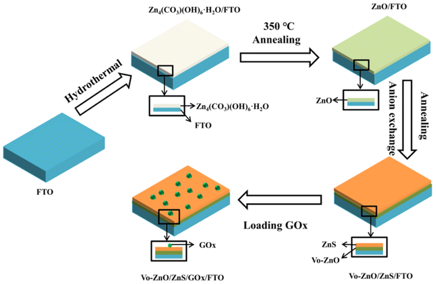 | ||
| Scheme 1 Simple schematic of the preparation process of the Vo-ZnO/ZnS/FTO electrodes and glucose sensor preparation. | ||
3. Results and discussion
3.1. Characterization of nanomaterials
The properties of two sets of photocatalytic materials, Vo-ZnO/ZnS and ZnO, were analyzed and compared, in which Vo-ZnO/ZnS was prepared by 0.21 M S2− in situ sulfidation and calcination at 300 °C. The phase analysis of the photocatalyst was performed using XRD, and the results are presented in Fig. S1† and 1. The peaks shown in Fig. S1† agree with Zn4(CO3)(OH)6·H2O (JCPDS 11-0287).5 After annealing, Zn4(CO3)(OH)6·H2O was decomposed into ZnO, as depicted in Fig. 1. As shown in Fig. 1, ZnO has a hexagonal wurtzite crystal structure (JCPDS 89-0511) with high crystallinity.18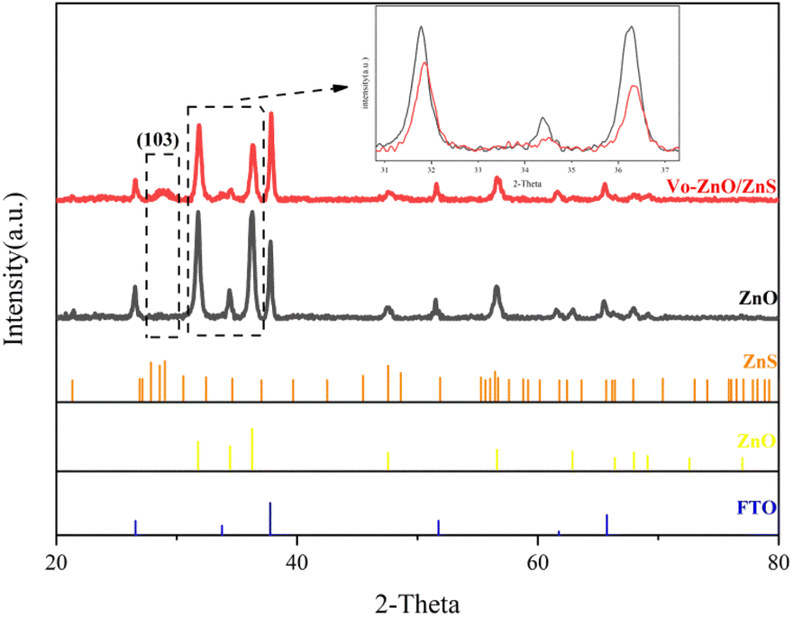 | ||
| Fig. 1 XRD spectra of the ZnO and Vo-ZnO/ZnS. | ||
After the in situ anionic sulfidation process, a new diffraction peak (103) was observed at 28.9° belonging to hexagonal ZnS (JCPDS 72-0163). The peak of ZnO in Vo-ZnO/ZnS also shifted to a higher angle, which suggested lattice distortion toward ZnO. According to a previous report,19 this phenomenon could be attributed to the strain effect between the two phases given the lattice mismatch between and ZnS. To reduce the lattice mismatch, more defect states appear in the interface of ZnO and ZnS according to thermodynamic law. The analysis of the defect states is presented hereinafter.
The microscopic morphology of the sample was investigated using SEM. The Zn4(CO3)(OH)6·H2O comprised uniform nanosheets that are relatively smooth (Fig. S2a–c†). The micromorphology of the ZnO nanoclusters (Fig. 2a, c and e) reveal that it is in the same nanoclusters as Zn4(CO3)(OH)6·H2O, but the ZnO nanosheets are made of closely packed nanoparticles. In contrast, the morphology of the Vo-ZnO/ZnS nanoclusters (Fig. 2b, d and f) indicates that the ZnS crystalline phase could not change the morphology of the ZnO during the growth process, and the morphology of Vo-ZnO/ZnS does not change significantly. Therefore, morphology was not the main factor in the improved performance of the Vo-ZnO/ZnS nanoclusters.
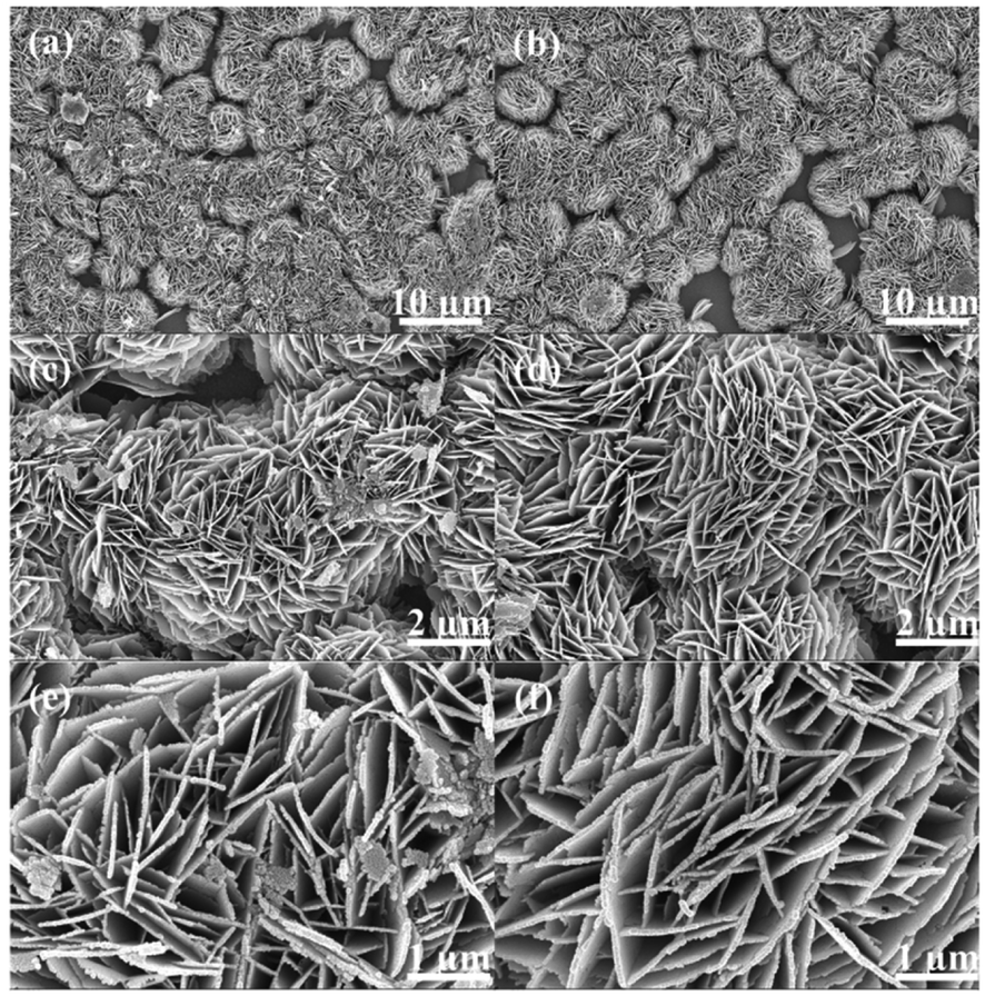 | ||
| Fig. 2 SEM images of ZnO (a, c and e) and Vo-ZnO/ZnS nanoclusters (b, d and f). | ||
The high magnification transmission electron microscopy (HRTEM) pattern of the Vo-ZnO/ZnS nanoclusters is shown in Fig. 3. The image suggests that Vo-ZnO/ZnS comprises small nanoparticles and is a porous material (Fig. 3a and b). As shown in Fig. 3c and d, the interplanar distances of 0.26 and 0.30 nm corresponded to the (002) crystal plane of ZnO and the (103) crystal plane of ZnS, respectively,20 suggesting that both ZnO and ZnS were in the sample. In addition, the poorly crystalline or amorphous regions between ZnO and ZnS are shown in Fig. 3d, suggesting the existence of a substantial number of defects in the interface. The appearance of the defect may arise from the stress between ZnO and ZnS and could cause lattice distortion between the interfaces of the two phases. To analyze the distribution of the elements, EDS was employed (Fig. 3e–h). According to the results, Zn, O, and S were equidistributed on the Vo-ZnO/ZnS surface.
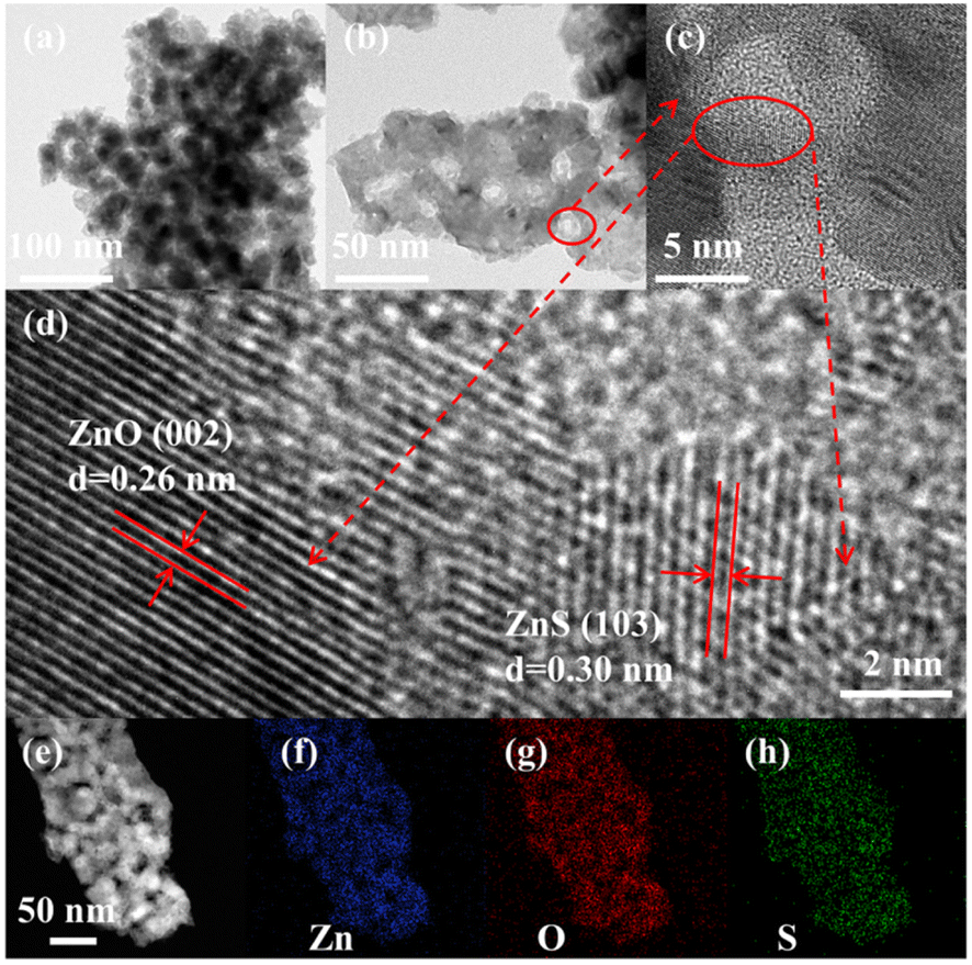 | ||
| Fig. 3 TEM images of Vo-ZnO/ZnS nanoclusters (a and b), HRTEM of Vo-ZnO/ZnS nanoclusters (c and d) and EDS elemental mapping images of Zn, O, and S (e–h). | ||
To analyze the surface element chemical state of ZnO and Vo-ZnO/ZnS, the survey-scanned XPS spectra of the Zn 2p, S 2p, and O 1s binding energies of the samples were investigated by XPS (Fig. 4). The survey spectra of ZnO and Vo-ZnO/ZnS (Fig. 4a) indicated that Zn and O were contained in ZnO and Vo-ZnO/ZnS, but S was only found in Vo-ZnO/ZnS. The peak positions (Fig. 4b) of Zn 2p1/2 and Zn 2p3/2 were 1044.4 and 1021.3 eV, respectively. The peak difference of 23.1 eV implied that Zn was in ZnO,8 which agrees with previous studies. Furthermore, the shift in the Zn 2p peak positions toward high binding energy for the Vo-ZnO/ZnS nanoclusters may arise from the preparation of ZnS, which could increase the binding energy of Zn 2p. As illustrated in Fig. 4c, positions 161.7 and 162.9 eV belonged to S 2p3/2 and S 2p1/2, respectively, and both were correlated with the Zn–S bond, indicating the synthesis of ZnS.18 The O 1s chemical elemental states of ZnO and Vo-ZnO/ZnS are shown in Fig. 4d, where the peaks at 530.1 and 531.5 eV represent the lattice oxygen and oxygen vacancies of ZnO,21 respectively. The oxygen vacancy intensity was evaluated by calculating the integral area ratio of the lattice oxygen and oxygen vacancy peaks, and the results showed that the oxygen vacancy ratio (0.503) in ZnO is significantly weaker than the oxygen vacancy ratio (1.97) in Vo-ZnO/ZnS. This finding indicates an improvement in oxygen vacancy after in situ sulfidation and annealing. Furthermore, the O 1s peak position shifted, suggesting the presence of electron transport between ZnO and ZnS22 and the formation of heterojunctions between ZnO and ZnS.
 | ||
| Fig. 4 XPS spectra of ZnO and Vo-ZnO/ZnS: (a) complete survey and (b) Zn 2p, (c) S 2p, and (d) O 1s peak. | ||
EPR could be used to investigate defects inside materials. The g values of Vo-ZnO/ZnS and ZnO are 2.0058 and 2.0057, respectively (Fig. 5a), which resulted from surface oxygen defects according to the literature results.23 Furthermore, the oxygen vacancy signal of Vo-ZnO/ZnS is significantly stronger than that of ZnO, which suggests a higher concentration of surface oxygen defects in Vo-ZnO/ZnS. This outcome was consistent with the XPS results.
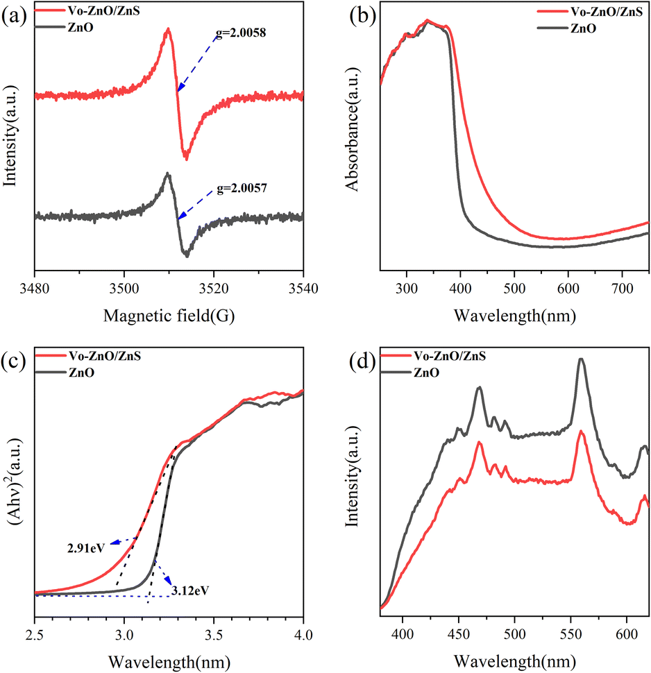 | ||
| Fig. 5 EPR spectra (a), UV-vis absorption spectra (b and c) and PL spectra (d). | ||
To understand the band gap of the two materials, the UV spectra of ZnO and Vo-ZnO/ZnS were investigated. Clearly, the absorption band edge of ZnO is in the UV spectral region and that of Vo-ZnO/ZnS shifted to the visible spectral region. The band gaps for ZnO and Vo-ZnO/ZnS were 3.12 and 2.91 eV, respectively, as calculated using Tauc’s plot (Fig. 5c). The narrowed band gap could be explained as follows: the lattice mismatch generates numerous active surface oxygen vacancies at the interface between ZnO and ZnS,18 which makes the absorption of the two wide-bandgap semiconductors24 combined to shift to the visible spectral region. This effect is very favorable for the improvement of photocatalytic activity.
PL intensity can also reflect the photogenerated carrier recombination strength of semiconductor materials.25 The fluorescence intensity (Fig. 5d) of Vo-ZnO/ZnS under UV irradiation is weaker than that of ZnO, implying the long life-time toward Vo-ZnO/ZnS, which, in turn, means that the heterojunction of the two phases could promote the carrier separation ability.
3.2. Photoelectrochemical performance of nanomaterials
The data in Fig. S3† show that different calcination temperatures and sulfidation concentrations significantly affect the photoelectric response of Vo-ZnO/ZnS and show a trend of enhancement, followed by weakening, where the material has better photocurrent intensity under 0.21 M S2−sulfuration and 300 °C calcination conditions. The photocurrent responses of ZnO and Vo-ZnO/ZnS are shown in Fig. 6a. The photocurrents of the two materials decay from a spike photocurrent (Im) to a stable photocurrent (Is) over time, and the stable photocurrent intensity of Vo-ZnO/ZnS is three times that of ZnO. Moreover, the Vo-ZnO/ZnS nanocluster has a larger spike current mainly because of the better ability of Vo-ZnO/ZnS to absorb light in the visible region.26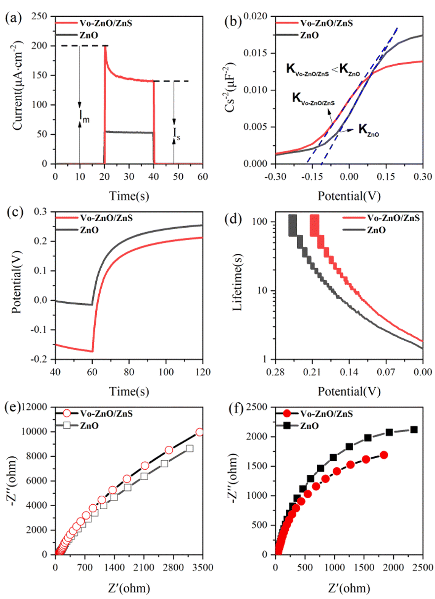 | ||
| Fig. 6 Photoelectric responses of the ZnO and Vo-ZnO/ZnS (a); Mott–Schottky plot of ZnO and Vo-ZnO/ZnS under dark conditions (b); open-circuit photovoltage decay curves (c) and lifetime of photogenerated carriers of the ZnO and Vo-ZnO/ZnS nanoclusters (d); Nyquist plots of the EIS of ZnO and Vo- ZnO/ZnS under (e) dark and (f) visible light illumination conditions. | ||
The Mott–Schottky (MS) test can be used to determine the type of semiconductor materials and the carrier density of semiconductors. In this study, the MS test was performed in the dark and fitted to the MS curves using eqn (1).27 As shown in Fig. 6b, ZnO and Vo-ZnO/ZnS are N-type semiconductors. The slope of the MS curves for ZnO (KZnO) is larger than that for the Vo-ZnO/ZnS nanoclusters (KVo-ZnO/ZnS), indicating that the carrier concentration of ZnO is lower than that of the Vo-ZnO/ZnS. A possible reason for this phenomenon is that Vo-ZnO/ZnS included relatively abundant surface oxygen vacancies, resulting in more lone electrons in the photocatalyst and leading to greater carrier density:
 | (1) |
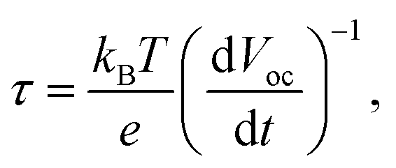
Subsequently, the OCP test (Fig. 6c and d) was used to analyze the lifetimes of different materials by applying eqn (2).5 The lifetime of Vo-ZnO/ZnS was longer than that of ZnO at the same bias voltage, suggesting that more electrons were assembled on the surface of Vo-ZnO/ZnS nanoclusters, making them more active in chemical reactions:16
 | (2) |
The carrier transport capacities of ZnO and Vo-ZnO/ZnS were examined by comparing the radii of the impedance arcs in the EIS spectra.28 As shown in Fig. 6e, the radius of the impedance arc for Vo-ZnO/ZnS increases compared with that of ZnO, which indicates that ZnO benefitted from carrier transport. However, the impedance arc radius of the Vo-ZnO/ZnS nanocluster is smaller than that of ZnO under light conditions (Fig. 6f), which indicates that the heterojunction formed by ZnO and ZnS promotes charge separation and the reduction of charge interfacial resistance.
3.3. Photoelectrochemical performance of nanomaterials
To investigate the potential applications of Vo-ZnO/ZnS in photoelectrochemical sensors, an AA-assisted glucose detection method was used (Scheme 2). According to previous studies, AA is commonly employed as a hole sacrificial agent in photocatalytic systems to improve photocatalytic efficiency.29 In this method, the reduction reaction between the AA and the hole excited by the semiconductor led to a significant increase in carrier utilization, resulting in an improved photovoltaic response of the photocatalyst (Fig. S4†). The detailed sensing mechanism is as follows: (1) light irradiating to Vo-ZnO/ZnS can generate photogenerated electron–hole pairs. (2) Owing to the surface oxygen defect that improves the light absorption ability of the material, the ability of the heterojunction to promote carrier separation makes the surface of the material pool more carriers to participate in the photocatalytic reaction; the addition of AA that has electron donor property, and the photocatalytic activity of the material is further improved. (3) When glucose is added to the above photocatalytic system, it decomposes into gluconic acid and hydrogen peroxide in the presence of glucoamylase and oxygen. Hydrogen peroxide reacts with the electrons pooled in the conduction band of ZnO, making the photocurrent intensity decrease. When AA is present in the photocatalytic system, the high redox hydrogen peroxide reacts with AA, making the intensity of the photocurrent enhanced by AA in (2) decrease. This phenomenon is directly demonstrated by the increased sensitivity of the material. AA also contributes to the stability of glucose detection30 because it could promptly consume hydrogen peroxide, which, in turn, adsorbs on the electrode surface and reduces enzyme activity.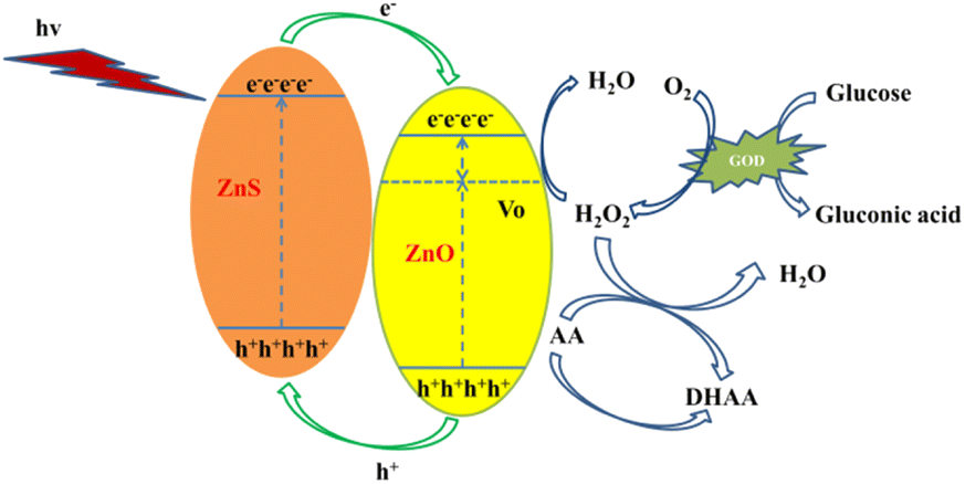 | ||
| Scheme 2 Detection mechanism for the Vo-ZnO/ZnS glucose photoelectrochemical sensor. | ||
According to the above detection strategy, a photoelectrochemical sensor toward glucose was built, and its performance is shown in Fig. 7. The photocurrent intensities of ZnO and Vo-ZnO/ZnS decrease to different degrees as the glucose concentration increased and exhibited different performances for glucose detection. In detail, the linear detection range of ZnO photoelectrochemical sensors is 0.2–0.8 mM, and the sensitivity is 15.7 μA cm−2 mM−1, with a detection limit of 29.9 μM (3N/S). For comparison, Vo-ZnO/ZnS photoelectrochemical sensors showed excellent comprehensive performance with longer linear detection ranges (0.2–1.2 mM and 1.4–3.0 mM), higher sensitivity (49.43 μA cm−2 mM−1 for low concentration and 17.64 μA cm−2 mM−1 for high concentration), and a detection limit of up to 15.5 μM (3N/S). According to these results, Vo-ZnO/ZnS is a better material for photoelectrochemical sensor applications.
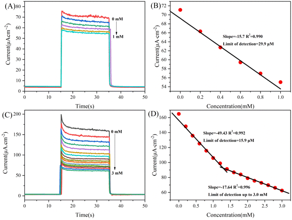 | ||
| Fig. 7 Photoelectrochemical responses with different concentrations of glucose of ZnO (A) and Vo-ZnO/ZnS (C) and the calibration curves between the photocurrent and the concentration of glucose of ZnO (B) and Vo-ZnO/ZnS (D). | ||
The glucose sensing performance of Vo-ZnO/ZnS was compared with the glucose sensors reported in recent years (Table S1†). By comparing with electrochemical sensors (Nafion/GOx/PtNDs/ZnONRs/ITO, GR/PANI:rGO/GOx, and graphene), Vo-ZnO/ZnS has a lower detection limit (15.9 μM), which may be due to the photoelectrochemical sensor's operating mode of optical signal excitation and electrical signal output. This can effectively reduce the background signal. Compared with the photoelectrochemical sensor (BiVO4/FTO, Fe2O3 films, ITO/MTiO2-Au NPs-MoS2-GOx), the advantage of ZnO in sensing sensitivity (49.43 μA cm−2 mM−1 for low concentration and 17.64 μA cm−2 mM−1 for high concentration) is more obvious, and the main reason here may be related to the construction of the material and the design of the sensing strategy. The properties of the electron donor AA, surface oxygen defects and heterojunctions synergistically improve the photocatalytic performance of the material, which makes Vo-ZnO/ZnS exhibit better sensitivity in glucose sensing. However, the detection limit of Vo-ZnO/ZnS is deficient relative to the photoelectrochemical sensors, which we believe is mainly due to surface oxygen defects. This is a highly reactive group that can improve the photocatalytic activity of the material but may cause instability during the sensing process, but we believe this is acceptable relative to the improved overall performance of the material.
To further evaluate the sensing performance of Vo-ZnO/ZnS, the experiment was repeated seven times in a glucose solution, and the data showed relatively good stability (Fig. S5a†). To investigate the anti-interference performance of the sensor, the photoelectric response of possible co-existing biomolecules (such as AA (b), suc (c), UA(d), NaCL (e), DA (f), TCD (g), Ur (h), lac (i), fru(j), cys (k), and gly(l)) added to the sensing test solution was investigated. The results showed that after 0.03 mM of interference, molecules were added to the sensing test solution containing 3 mM of glucose (a). The interference induced photocurrent changes of 0.85%, 1.3%, 5.1%, 4.2%, 2.5%, 0.99%, 1.2%, 2.3%, 3.5%, 3.2%, and 3.6%. These experimental results (Fig. S5b†) indicate that the photoelectrode has good interference immunity performance.
4. Conclusions
In this study, oxygen-defect-rich Vo-ZnO/ZnS heterojunctions were successfully prepared using hydrothermal and ion exchange techniques and calcination in a nitrogen environment. The Vo-ZnO/ZnS nanocluster heterojunctions with abundant oxygen defects have enhanced visible light absorption, high carrier lifetime, high carrier concentration, and low solution semiconductor interfacial resistance. These advantages make the Vo-ZnO/ZnS nanocluster heterojunctions have better photoelectrochemical performance. Finally, the results of sensing tests on glucose show that the Vo-ZnO/ZnS nanocluster heterojunction is a better photocatalytic material and can be applied to photoelectrochemical sensors.Conflicts of interest
The authors declare that they have no competing interests.Acknowledgements
This research was financially supported by the Hainan Province Science and Technology Special Fund (No. ZDYF2021SHFZ068 and ZDKJ2021029), the National Natural Science Foundation of China (No. 52262014), the Hainan Provincial Natural Science Foundation of China (No. 823CXTD376), CAMS Innovation Fund for Medical Sciences (No. 2019-I2M-5-023), Key Laboratory Open Project Fund of Emergency and Trauma of Ministry of Education (No. KLET-202110), and Hainan Province Clinical Medical Center.Notes and references
- C. Lops, A. Ancona, K. Di Cesare, B. Dumontel, N. Garino, G. Canavese, S. Hernandez and V. Cauda, Appl. Catal., B, 2019, 243, 629–640 CrossRef CAS PubMed.
- X. Zhao, J. Feng, J. Liu, J. Lu, W. Shi, G. Yang, G. Wang, P. Feng and P. Cheng, Adv. Sci., 2018, 5, 1700590 CrossRef PubMed.
- D. Zhao, Y. Zhang, S. Ji, Y. Lu, X. Bai, M. Yin, C. Huang and N. Jia, Biosens. Bioelectron., 2020, 173, 112816 CrossRef PubMed.
- J. Sun, Z. Chen, C. Xu, B. Jin, Z. Guo, X. Wang, N. He and M. Wang, Biosens. Bioelectron., 2022, 214, 114491 CrossRef CAS PubMed.
- D. Chen, X. Zou, F. Dong, C. Zhen, D. Xiao, X. Wang, Q. Wu, Y. Cao and J. Tu, ACS Appl. Mater. Interfaces, 2021, 13, 33006–33014 CrossRef CAS PubMed.
- N. P. Shetti, S. D. Bukkitgar, K. R. Reddy, C. V. Reddy and T. M. Aminabhavi, Biosens. Bioelectron., 2019, 141, 111417 CrossRef CAS PubMed.
- D. Chen, L. Lv, L. Peng, J. Peng, Y. Cao, X. Wang, X. Wang, Q. Wu and J. Tu, Ceram. Int., 2019, 45, 18044–18051 CrossRef CAS.
- Y. Wang, H. Ping, T. Tan, W. Wang, P. Ma and H. Xie, RSC Adv., 2019, 9, 28165–28170 RSC.
- X. Wang, G. Li, J. Peng, X. Lai, Q. Wu, Y. Cao, L. Ding and J. Tu, J. Alloys Compd., 2021, 873, 159721 CrossRef CAS.
- P. Kalisamy, M. Lallimathi, M. Suryamathi, B. Palanivel and M. Venkatachalam, RSC Adv., 2020, 10, 28365–28375 RSC.
- J. Jiang, G. Wang, Y. Shao, J. Wang, S. Zhou and Y. Su, Chin. J. Catal., 2022, 43, 329–338 CrossRef CAS.
- M. Kwiatkowski, I. Bezverkhyy and M. Skompska, J. Mater. Chem. A, 2015, 3, 12748–12760 RSC.
- W. Zhang, Y. Sun, Z. Xiao, W. Li, B. Li, X. Huang, X. Liu and J. Hu, J. Mater. Chem. A, 2015, 3, 7304–7313 RSC.
- S. Feng, T. Wang, B. Liu, C. Hu, L. Li, Z. J. Zhao and J. Gong, Angew. Chem., 2020, 59, 2044–2048 CrossRef CAS PubMed.
- H. L. Guo, Q. Zhu, X. L. Wu, Y. F. Jiang, X. Xie and A. W. Xu, Nanoscale, 2015, 7, 7216–7223 RSC.
- Q. Ding, D. Xu, J. Ding, W. Fan, X. Zhang, Y. Li and W. Shi, J. Colloid Interface Sci., 2021, 603, 120–130 CrossRef CAS PubMed.
- Q. Zhang, X. Zhao, L. Duan, H. Shen and R. Liu, J. Photochem. Photobiol., A, 2020, 392, 112156 CrossRef CAS.
- K. S. Ranjith, R. B. Castillo, M. Sillanpaa and R. T. Rajendra Kumar, Appl. Catal., B, 2018, 237, 128–139 CrossRef CAS.
- F. Yu, Y. Zhou, J. Cui, Z. Liu, Y. Li, L. He, J. Zhang, X. Tang and Y. Liu, J. Mater. Sci., 2022, 57, 983–1005 CrossRef CAS.
- Y. Piña-Pérez, O. Aguilar-Martínez, P. Acevedo-Peña, C. E. Santolalla-Vargas, S. Oros-Ruíz, F. Galindo-Hernández, R. Gómez and F. Tzompantzi, Appl. Catal., B, 2018, 230, 125–134 CrossRef.
- F. Qiao, K. Sun, W. Liu, Y. Xie and H. Chu, Vacuum, 2022, 196, 110788 CrossRef CAS.
- C. Li, S. Chen, Y. Wang and Z. Hou, Int. J. Hydrogen Energy, 2019, 44, 25416–25427 CrossRef CAS.
- Y. Xu, H. Li, B. Sun, P. Qiao, L. Ren, G. Tian, B. Jiang, K. Pan and W. Zhou, Chem. Eng. J., 2020, 379, 122295 CrossRef CAS.
- C. Huo, T. Wang, Z. Yin, X. Xu, J. He and S. Cao, Ceram. Int., 2023, 49, 14673–14680 CrossRef CAS.
- F. Gao, J. Yuan, X. Huang, R. Lei, C. Jiang, J. Zhuang and P. Liu, Chem. Eng. J., 2021, 416, 129159 CrossRef CAS.
- W. Xia, L. Guan, X. Zeng, J. Yang, H. He and Y. Cao, J. Phys. D: Appl. Phys., 2019, 52, 035501 CrossRef.
- J. Ma, M. Zhang, W. Su, B. Wu, Z. Yang, X. Wang, B. Qiao, H. Pei, J. Tu, D. Chen and Q. Wu, Langmuir, 2022, 38, 751–761 CrossRef CAS PubMed.
- X. Zhang, D. Yue, L. Zhang and S. Lin, J. Mater. Sci. Technol., 2020, 56, 162–169 CrossRef CAS.
- Q. Zhang, X. Liu, H. Wang, Q. Liu, Q. Liu and X. Zhang, Analyst, 2021, 146, 855–863 RSC.
- D. Chen, X. Wang, K. Zhang, Y. Cao, J. Tu, D. Xiao and Q. Wu, Biosens. Bioelectron., 2020, 166, 112466 CrossRef CAS PubMed.
Footnote |
| † Electronic supplementary information (ESI) available: Reagents and apparatus, photoelectrochemical and glucose sensing testing; Fig. S1: XRD spectra of Zn4(CO3)(OH)6·H2O, Table S1: Comparison of analytical performances of glucose sensors; Fig. S2: SEM images of Zn4(CO3)(OH)6·H2O (a–c); Fig. S3: effect of temperature (a) and sodium sulfide concentration (b) on the photoelectric response of Vo-ZnO/ZnS; Fig. S4: photoelectric response of ZnO and Vo-ZnO/ZnS with and without AA; Fig. S5: stability test of Vo-ZnO/ZnS under the absence of 3 mM glucose condition (a); influence of interferences on the photoelectric response (b). See DOI: https://doi.org/10.1039/d3ra02869k |
| This journal is © The Royal Society of Chemistry 2023 |