
 Open Access Article
 This Open Access Article is licensed under a Creative Commons Attribution-Non Commercial 3.0 Unported Licence
Oxygen functionalized InSe and TlTe two-dimensional materials: transition from tunable bandgap semiconductors to quantum spin Hall insulators†
Qing Lu a,
Lin Lia,
Shilin Luoa,
Yue Wanga,
Busheng Wang*b and
Fu-Ti Liu*a
a,
Lin Lia,
Shilin Luoa,
Yue Wanga,
Busheng Wang*b and
Fu-Ti Liu*a
aKey Laboratory of Computational Physics of Sichuan Province, Faculty of Science, Yibin University, Yibin 644000, China. E-mail: futiliu@163.com
bDepartment of Chemistry, State University of New York at Buffalo, Buffalo, NY 14260-3000, USA. E-mail: bushengw@buffalo.edu
First published on 21st June 2023
Abstract
From first-principles calculations, we found that oxygen functionalized InSe and TlTe two-dimensional materials undergo the following changes with the increased concentrations of oxygen coverage, transforming from indirect bandgap semiconductors to direct bandgap semiconductors with tunable bandgap, and finally becoming quantum spin hall insulators. The maximal nontrivial bandgap are 0.121 and 0.169 eV, respectively, which occur at 100% oxygen coverage and are suitable for applications at room temperature. In addition, the topological phases are derived from SOC induced p–p bandgap opening, which can be further determined by Z2 topological invariants and topologically protected gapless edge states. Significantly, the topological phases can be maintained in excess of 75% oxygen coverage and are robust against external strain, making the quantum spin hall effect easy to achieve experimentally. Thus, the oxygen functionalized InSe and TlTe are fine candidate materials for the design and fabrication of topological devices.
1. Introduction
Group III sulfur compound layered materials have become a research hotspot1,2 due to their high carrier mobility, p-type electronic behavior and wide-cap shaped band edges. Their layered or monolayer materials (GaS, GaSe and InSe) have been experimentally realized,3–5 forming a new class of two-dimensional (2D) materials. These 2D materials can be used as candidates for optoelectronic devices and electronic devices,6–8 where field effect transistors made with monolayer InSe have high carrier mobility and large switching ratio,6,7 photodetectors made with GaS,4 GaSe,5 GaTe,9 InSe10 and TlTe11 show high photoresponsiveness and fast response time. In addition, these 2D materials have potential applications in thermoelectric,12 piezoelectric13 and electrocatalytic fields.14Quantum spin hall (QSH) insulators, which is called 2D topological insulators, was first proposed in graphene15,16 and then experimentally achieved in HgTe/CdTe17,18 and InAs/GaSb19,20 quantum wells. Chemically functionalized 2D materials are an effective way to modulate structural and electronic properties.21–24 Halogenation, hydrogenation, methyl and ethynyl functionalization, oxidation of 2D materials have been studied in theoretical detail, with tunable electronic and topological properties. With halogenation and hydrogenation, germanene,25,26 stanene,26–28 phosphene,29 arsenene,30,31 antimonene32 and bismuthene33 as well as binary compounds with inversion asymmetry31,34–40 are 2D topological insulators with large bandgap, with the largest bandgap reaching 1.08 eV. In addition, methyl functionalized stanene,41,42 arsenene43 and bismuthene,44 as well as ethynyl functionalized stanene45 can further improve the nontrivial topological bandgap. Finally, with oxygen functionalization, arsenene,46 antimonene47 and bismuthene48 can also achieve QSH insulators with large bandgap. All of these topological insulators have the potential for room-temperature applications.
Despite the considerable properties of group III sulfur compounds, few studies have focused on their chemical modification. Oxidized InSe monolayer by heat treatment, Balakrishnan et al. obtained the InSe/In2O3 heterojunction and found that it could be used as a p–n junction with tunable bandgap.49 Researchers have also found that oxidized GaSe and GaTe films could lead to a decrease in photoluminescence.50,51 Monolayer InSe has rich electronic and optical properties, which can obtain nontrivial topological phases through full oxygen coverage.52 Considering that partial oxygen coverage may occur under experimental conditions, it is of great significance to study the electronic and topological properties of InSe 2D materials with different concentrations of oxygen coverage. Among the group III elements, Tl and Te elements have stronger spin–orbit coupling (SOC) than In and Se elements, respectively, and should be able to further induce and stabilize their topological phases.
In this paper, we have studied InSe and TlTe 2D materials with different concentrations of oxygen coverage through 2 × 2 supercell. The InSe changes from an indirect bandgap semiconductor to a direct bandgap semiconductor at 25% oxygen coverage (InSeO0.25), and the bandgap is decreased from 1.392 eV to 0.636 eV. The InSe also keeps a direct bandgap semiconductor at 50% oxygen coverage (InSeO0.5) with the bandgap further reduced to 0.123 eV, transforming into a QSH insulator at 75% oxygen coverage (InSeO0.75). The 2D material InSe at 100% oxygen coverage, namely InSeO, has a nontrivial bandgap of 0.121 eV, which is suitable for applications at room temperature. The oxygen functionalized TlTe shows the same trend as the oxygen functionalized InSe. With the increased concentrations of oxygen coverage, the TlTe changes from an indirect bandgap semiconductor to a direct bandgap semiconductor, and turns into a QSH insulator at 75% oxygen coverage (TlTeO0.75). The TlTe 2D material at 100% oxygen coverage (TlTeO) has a nontrivial bandgap increased to 0.169 eV due to the strong SOC of Tl elements. Their topological phases are derived from SOC-induced p–p bandgap opening and can be further determined by Z2 topological invariants and topologically protected gapless edge states.
2. Theoretical methods and computational details
First-principles calculations were performed using the projected augmented wave (PAW) method53 as implemented in the Vienna ab initio simulation package (VASP).54 The exchange-correlation energy was treated using Perdew–Burke–Ernzerhof (PBE)55 generalized gradient approximation. The energy cutoff of the plane wave basis was selected as 500 eV with an energy precision of 10−5 eV. Meanwhile, 11 × 11 × 1 K point grid56 was selected for Brillouin-zone sampling. All atoms are relaxed until the force on each atom is lower than 0.01 eV Å−1. The setting of these parameters is sufficient to ensure the accuracy of structure optimization. For self-consistent and energy band calculations, the energy cutoff of plane wave basis was remained as 500 eV, with energy precision improved to 10−6 eV, and the Brillouin-zone sampling was increased to 15 × 15 × 1 K point grid. The influence of SOC was taken into account in all the processes starting from static self-consistent calculation. Phonopy57 based on density functional perturbation theory was used to calculate the phonon spectra. The Wannier90 function58 combined with WannierTools59 was used to calculate the topological invariant Z2 and topologically protected edge states.3. Results and discussion
3.1 Crystal and electronic structures of oxygen functionalized InSe
The crystal of InSe contains two layers of In atoms between two layers of Se atoms, which can be regarded as two layers of InSe with hexagonal honeycomb shape connected by In atoms, as shown in Fig. 1(a). Therefore, an InSe primitive cell contains two In and Se atoms. After structure optimization, the lattice constant a, the bond length dIn–Se formed by In and Se atoms, and the bond length dIn–In formed between In atoms are 4.085, 2.682 and 2.824 Å, respectively. The calculated band structure of InSe is shown in Fig. 1(b). It is obvious that the valence band top is located between Γ and K points, while the conduction band bottom is located at Γ point, forming an indirect bandgap of 1.392 eV, which has the characteristics of semiconductor. In addition, the valence band top and the conduction band bottom have a wide brimmed hat and a parabolic shape, respectively. By constructing 2 × 2 supercells of InSe, and adsorbing O atoms simultaneously on Se atoms at both ends, we can study the effect of oxygen coverage at different concentrations.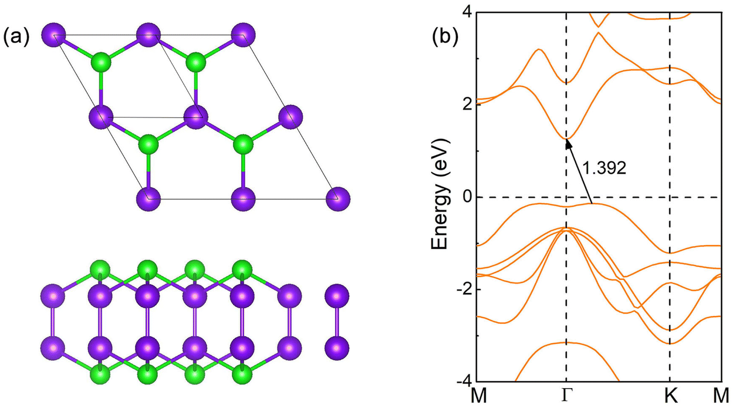 | ||
| Fig. 1 (a) Top view and side view of the structure of InSe 2D material. The blue and green spheres represent In and Se atoms, respectively. The small square represents one of the primitive cells. (b) The band structure of InSe with the bandgap size. | ||
The structure and band structure of InSe at 25% oxygen coverage (InSeO0.25) are shown in Fig. 2(a). Compared with InSe, we adsorb O atoms simultaneously on Se atoms at both ends of a single cell. After structure optimization, the lattice constant a and the bond length dSe–O of InSeO0.25 are 8.263 and 1.679 Å, respectively, as shown in Table 1. The band structure of InSeO0.25 changes from indirect bandgap to direct bandgap with the bandgap also decreasing from 1.392 eV to 0.636 eV. For InSe 2D materials at 50% oxygen coverage (InSeO0.5), we adsorbed O atoms simultaneously on Se atoms at both ends of two single cells. After structure optimization, the lattice constant a of InSeO0.5 is 8.423 Å and the bond length dSe–O formed by Se and O atoms is 1.688 Å. The InSeO0.5 2D material is still a direct bandgap semiconductor with the bandgap further reduced to 0.123 eV, as shown in Fig. 2(b).
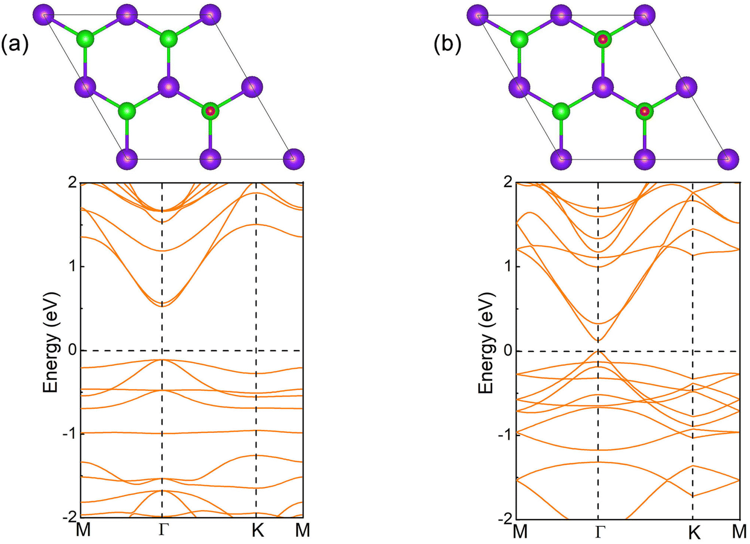 | ||
| Fig. 2 Top view and calculated band structure of the oxygen functionalized InSe. (a) InSeO0.25, and (b) InSeO0.5. The blue, green and red balls represent In, Se and O atoms respectively. | ||
| InSeO0.25 | InSeO0.50 | InSeO0.75 | InSeO | |
|---|---|---|---|---|
| a | 8.263 | 8.423 | 8.67 | 4.478 |
| dSe–O | 1.679 | 1.688 | 1.683 | 1.68 |
For InSe 2D material at 75% oxygen coverage (InSeO0.75), we adsorbed O atoms simultaneously on Se atoms at both ends of three single cells. After structure optimization, the lattice constant a of InSeO0.75 is 8.67 Å and the bond length dSe–O formed by Se and O atoms is 1.683 Å, as shown in Table 1. From the band structure and the orbital projection band structure of InSeO0.75, it can be seen that the two px,y orbitals are degenerated at the Γ point of Fermi level and occupy the conduction band bottom and the valence band top, showing the gapless semi-metallic characteristics in the absence of SOC. After considering the SOC, the two degenerate px,y orbitals are split apart, with one degenerate px,y orbital moving up, the other degenerate px,y orbital moving down, as shown in Fig. 3(a) and 4(a). Thus, the SOC induced p–p bandgap opening occurs in InSeO0.75. Both px,y orbitals exhibit parabolic quasi-quadratic dispersion relations and there are still very few s and pz orbitals above and below the two px,y orbitals.
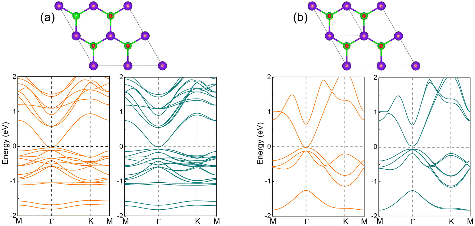 | ||
| Fig. 3 Structure and band structure of (a) InSeO0.75 and (b) InSeO. Orange and dark gray curves represent the band structures without and with SOC, respectively. The blue, green and red balls represent In, Se and O atoms respectively. | ||
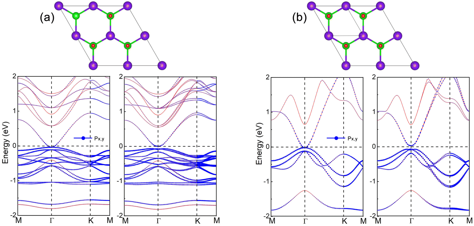 | ||
| Fig. 4 Structure and orbital projected band structure of (a) InSeO0.75 and (b) InSeO. The left and right sides represent the band structures without and with SOC, respectively. The blue circle represents the px,y orbitals, with the size of the circle corresponding to the weight of the projected orbit. | ||
For InSe 2D material at 100% oxygen coverage (InSeO), O atoms are simultaneously adsorbed on Se atoms at both ends of four single cells. However, a single cell is still used in the calculation. The lattice constant a of the optimized InSeO, the bond lengths dIn–Se formed by In atoms and Se atoms, and the bond lengths dIn–In formed between In atoms are increased to 4.478, 2.826 and 2.931 Å. The bond formed by Se and O atoms is perpendicular to InSe to reduce the influence of Coulomb repulsion. The bond length dSe–O is 1.68 Å, and the corresponding bond overlap number is 0.58, indicating that Se and O atoms are covalently bonded. Just like InSeO0.75, when SOC is not considered, two degenerate px,y orbitals occupy the Fermi level, showing the gapless semi-metallic characteristics. After considering the SOC, the two degenerate px,y orbitals are split, and p–p bandgap opening appears, as shown in Fig. 3(b) and 4(b). The parabolic shape of the two px,y orbitals is much more pronounced, and there are also very few s and pz orbitals above and below the two px,y orbitals.
Wang et al. used the three orbitals s, px and py as the minimum basis to construct tight-binding model in triangular lattice.60 They confirmed that QSH phase can originate from two mechanisms, namely, SOC induced s–p band inversion or SOC induced p–p bandgap opening. For the first mechanism, the s orbital is above the p orbital, and after considering the SOC, a degenerate p and s orbital are reversed, resulting in the formation of the QSH phase. For the second mechanism, the p orbitals are degenerated at the Γ point, and when SOC is taken into account, the p–p bandgap opens and the QSH phase is generated. The second mechanism was also proposed by Liang et al.61 They used multiple p orbitals, mainly px and py orbitals, to construct the k·p model, and proved that multiple p orbitals would exhibit degenerate and quasi-quadratic band dispersion at Γ point, and when SOC is included, the p–p bandgap would open and generate nontrivial topological phase. Thus, for InSeO0.75 and InSeO 2D materials, their QSH phases arise from SOC induced p–p bandgap opening. The systems with the same mechanism include Au on GaAs(1 1 1) surface,60 Bi on Si(1 1 1) surface, Bi-AU-H on SiC(1 1 1) surface61 and Bi/Ag on Si(1 1 1) surface.62 The nontrivial bandgap of InSeO is 0.097 eV, which is sufficient for room temperature applications. As the PBE functional55 usually underestimate the bandgap, the HSE06 functional63 is employed to correct the bandgap. In the absence of SOC, the InSeO maintains semi-metallic characteristics with HSE06. After considering the SOC, the nontrivial band gap of InSeO is increased to 0.121 eV, as shown in Fig. S1.† We also employ G0W0 method21–24 to calculate the band gap of InSeO, which further increased to 0.351 eV.
Oxygen functionalized InSe provide the opportunity to modulate the band gap. To reveal the origin of these electronic properties, we examine the partial charge densities of the functionalized InSe, as illustrated in Fig. S2.† Pristine InSe have the top valence band (VB) originated from the pz orbitals of In and Se atoms, and the bottom conduction band (CB) dominated by the s orbitals of both atoms. Accordingly, the top VB charge densities exhibit the pz orbital character, while the bottom CB charge densities are accumulated in between the In and Se atoms showing the in-plane σ bond character. In contrast, InSeO monolayers have the top VB and bottom CB both dominated by the px and py orbitals of In, Se, and O atoms. The partial charge densities of the bands are localized individually on the Se and O atoms, indicating the occupancy of antibonding states between Se and O atoms that leads to the narrowing of band gap.
We use the following formula to calculate the formation energy of InSeO![[thin space (1/6-em)]](https://www.rsc.org/images/entities/char_2009.gif) :Ef = E(InSeO) − E(InSe) + E(O), where E(InSeO) is the total energy of InSeO, E(InSe) is the total energy of InSe, and E(O) is the chemical potential of O atom. The calculated formation energy for InSeO is −2.774 eV. Therefore, O atoms are strongly bound to InSe through chemical bonding, and InSeO exhibit high thermodynamic stability. Correspondingly, the InSeO0.25, InSeO0.5 and InSeO0.75 are also thermodynamically stable. In Fig. 5, the phonon spectra of InSe and InSeO are also calculated. It can be seen that although the InSe has been synthesized experimentally, there is still a little virtual frequency at its Γ point. However, InSeO has no virtual frequency in the whole Brillouin area, which indicates that InSeO is dynamically stable. Therefore, the stability of InSe 2D material can be improved by oxygen functionalization. To further inspect the thermal stability of InSeO, we carry out ab initio molecular dynamics simulations (MD) with 4 × 4 × 1 supercell. The snapshot of atomic configuration at 300 K is plotted for InSeO at 2 ps, as illustrated in Fig. S3.† Neither structure reconstruction nor structure disruption appeared in InSeO, indicating that InSeO possess good thermal stability and maintains structural integrity at room-temperature. Like oxygen functionalized graphene,64 oxygen functionalized InSe 2D materials also hold great promise for synthesis by oxygen plasma technology.
:Ef = E(InSeO) − E(InSe) + E(O), where E(InSeO) is the total energy of InSeO, E(InSe) is the total energy of InSe, and E(O) is the chemical potential of O atom. The calculated formation energy for InSeO is −2.774 eV. Therefore, O atoms are strongly bound to InSe through chemical bonding, and InSeO exhibit high thermodynamic stability. Correspondingly, the InSeO0.25, InSeO0.5 and InSeO0.75 are also thermodynamically stable. In Fig. 5, the phonon spectra of InSe and InSeO are also calculated. It can be seen that although the InSe has been synthesized experimentally, there is still a little virtual frequency at its Γ point. However, InSeO has no virtual frequency in the whole Brillouin area, which indicates that InSeO is dynamically stable. Therefore, the stability of InSe 2D material can be improved by oxygen functionalization. To further inspect the thermal stability of InSeO, we carry out ab initio molecular dynamics simulations (MD) with 4 × 4 × 1 supercell. The snapshot of atomic configuration at 300 K is plotted for InSeO at 2 ps, as illustrated in Fig. S3.† Neither structure reconstruction nor structure disruption appeared in InSeO, indicating that InSeO possess good thermal stability and maintains structural integrity at room-temperature. Like oxygen functionalized graphene,64 oxygen functionalized InSe 2D materials also hold great promise for synthesis by oxygen plasma technology.
 | ||
| Fig. 5 Phonon spectrum of (a) InSe and (b) InSeO. | ||
3.2 Crystal and electronic structures of oxygen functionalized TlTe
After structure optimization, the lattice constant a of TlTe 2D material is 4.535 Å, the bond length dTl–Te formed by Tl atoms and neighboring Te atoms and the bond length dTl–Tl formed between the upper and lower layers of Tl atoms are 2.963 and 2.922 Å, respectively. The calculated band structure is shown in Fig. 6(a), same as InSe, the valence band top is located between the Γ and K points, and the conduction band bottom is located at Γ point, forming an indirect bandgap of 0.433 eV with a semiconductor characteristic. | ||
| Fig. 6 Structure and band structure of (a) TlTe, (b) TlTeO0.5 and (c) TlTeO. Orange and dark gray curves represent the band structures without and with SOC, respectively. The blue, green and red balls represent Tl, Te and O atoms, respectively. | ||
For TlTe at 50% oxygen coverage (TlTeO0.5), the lattice constant a and the bond length dTe–O formed by Te and O atoms are 9.4 and 1.854 Å, respectively. The bandgap of TlTeO0.50 changes from the indirect bandgap to the direct bandgap, and the bandgap also decreases from 0.433 eV to 0.152 eV, as shown in Fig. 6(b). For TlTe 2D material at 100% oxygen coverage (TlTeO), the lattice constant a, the bond length dTe–O of Te and O atoms, the bond length dTl–Te of Tl atoms and neighboring Te atoms, and the bond length dTl–Tl between the upper and lower layers of the Tl atoms are 5.032, 1.848, 3.135 and 3.104 Å, respectively. When the SOC is not considered, the two px,y orbitals are degenerated at the Fermi level Γ point, exhibiting the semi-metallic characteristics. After considering the SOC, two degenerate px,y orbitals are split apart, accompanied by the p–p bandgap opening, as shown in Fig. 6(c), indicating that TlTeO is the QSH insulator. Since the SOC intensity of Tl is larger than that of In, the nontrivial bandgap of TlTeO is increased to 0.124 eV by PBE functional55 (or 0.169 eV by HSE06 functional63), which has the more potential to be applied at room temperature, as shown in Fig. S1.† In fact, TlTe also become QSH insulator at 75% oxygen coverage (TlTeO0.75). However, the bandgap induced by the SOC is extremely small, which is easily destroyed by the thermally excited charge carriers. Thus, in terms of device application, it is better to choose the TlTeO. The calculated formation energy of TlTeO is −3.98 eV, which is larger than that of InSeO. It also shows great thermodynamic stability, so TlTeO has great hope of being synthesized by oxygen plasma technology.64 The snapshot of atomic configuration at 300 K is also plotted for TlTeO, as illustrated in Fig. S3.† Neither structure reconstruction nor structure disruption appeared in TlTeO.
3.3 Z2 topological invariants and topologically protected edge states
The topological properties of 2D materials can be determined by Z2 topological invariants and topologically protected edge states. In orbital projection, px and py orbitals have a great influence on the energy bands close to the Fermi level and the topological properties of the system, which are must be considered. However, there are still a small number of s and pz orbitals in the selected energy range, which will affect the overall smoothness of the projected bands, and should also be considered. After the projection orbitals are set, the Wannier90 function58 combined with VASP53 is used to calculate and generate Wannier function. By adjusting the freezing window, resolving entanglement window and related parameters, a good tight-binding model will be acquired. Finally, the obtained tight-binding model is brought into the WannierTools59 for calculation.Using WannierTools software to calculate the evolution of Wannier Charge Center (WCC),65 Z2 topological invariants can be obtained to identify the topological states. For InSeO and TlTeO 2D materials, the calculated Z2 topological invariants are 1, which confirms that they are both QSH insulators. The topologically protected edge states in bulk gap are also intuitive representations of the topological properties. Using iterative Green's function59 embedded in the WannierTools, we can obtain topologically protected edge states of InSeO and TlTeO, as shown in Fig. 7(a) and (b). Their edge states connect the valence and conduction bands and cross the Fermi level from X point to G point odd number of times, further confirming that InSeO and TlTeO are QSH insulators. These edge states are protected from backscattering by time-inversion symmetry and can ensure non-dissipative electron transport.62
 | ||
| Fig. 7 Topologically protected edge states of (a) InSeO and (b) TlTeO. | ||
3.4 Bandgap variation and orbital evolution under strain
Strains can effectively regulate the electronic and topological properties of 2D materials.66–73 The strains in InSeO and TlTeO can be defined as Ɛ = (a – a0)/a0, where a0 and a denote lattice constants at equilibrium and under strains, respectively. The changes of the bandgap EΓ-with and Eg-with under strains are shown in Fig. 8(a) and (b), where EΓ-with represents the direct bandgap at the Γ point under SOC and Eg-with represents the global bandgap under SOC. For InSeO, EΓ-with increases slowly with strains and reaches a maximum value of 0.121 eV at 7% strain. Eg-with increases monotonically with strains at first, reaches a maximum value of 0.102 eV at 3% strain, and then decreases monotonically with strains. The EΓ-with and Eg-with are consistent at −9% to 2% strains, and the band of InSeO shows a direct bandgap. Under other strains, the EΓ-with and Eg-with are separated from each other, and the band of InSeO appears as an indirect bandgap. When the strains are greater than 6%, the value of Eg-with is less than 0, and InSeO exhibits semi-metallic characteristics. For TlTeO, EΓ-with and Eg-with show the same trend as InSeO. The maximum value of EΓ-with is 0.172 eV at 9% strain, and the maximum value of Eg-with is 0.128 eV at 1% strain. The EΓ-with and Eg-with are consistent under strains of −4% to 1%, and the band of TlTeO shows a direct bandgap. When the applied strains are greater than 5%, the value of Eg-with is less than 0, and TlTeO exhibits semi-metallic characteristics. | ||
| Fig. 8 The bandgaps EΓ-with and Eg-with of (a) InSeO and (b) TlTeO change with strain. EΓ-with represents the direct bandgap at the Γ point under SOC and Eg-with represents the global bandgap under SOC. (c) Orbital evolution of InSeO and TlTeO under strain. (d) Band structure of InSeO at 7% tensile strain considering the SOC. (e) Band structure of TlTeO at 6% tensile strain considering the SOC. | ||
Next, we will analyze the evolution of orbitals under strains. Since O atoms hybridize with pz orbitals in the same energy range, pz orbitals leave the Fermi level, so px,y orbitals are mainly left around the Fermi level. Chemical bonding causes px,y orbitals to split into bonded and antibonded states |px,y±〉, where ± represents the bonded and antibonded states, respectively. When SOC is not considered, the |px,y+〉 state are occupied at the Fermi level, exhibiting semi-metallic characteristics. After considering the SOC, the |px,y+〉 are further split into |px+iy,↑+, px−iy,↓+〉 and |px−iy,↑+, px+iy,↓+〉, with |px+iy,↑+, px−iy,↓+〉 moving up and |px−iy,↑+, px+iy,↓+〉 moving down, so that a large energy gap opens and the QSH phase is generated, as shown in Fig. 8(c). It is obvious that once the SOC is taken into account, the p–p bandgap can be opened, with the generation of QSH phase. However, when the applied strains are greater than 6% and 5%, respectively, the valence band top at point K rises above the Fermi level, so that InSeO and TlTeO become semi-metallic again, as shown in Fig. 8(d) and (e).
4. Conclusions
By constructing InSe and TlTe 2 × 2 supercells, the structure, electronic and topological properties of oxygen functionalized InSe and TlTe are studied. With the increased concentrations of oxygen coverage, the InSeO0.25, InSeO0.5 and InSeO0.75, experience the transformation from indirect bandgap semiconductor to direct bandgap semiconductor and finally to QSH insulator. The nontrivial bandgap of InSeO is 0.121 eV, which owns potential applications at room temperature. The oxygen functionalized TlTe shows the same trend as the oxygen functionalized InSe. Due to the stronger SOC, the nontrivial bandgap of TlTeO is increased to 0.169 eV. In addition, the QSH phases in oxygen functionalized InSe and TlTe are derived from SOC induced p–p bandgap opening. Significantly, the QSH phases can be maintained in excess of 75% oxygen coverage and are robustly against the external strain, making the QSH effect easy to be achieved experimentally. Thus, the oxygen functionalized InSe and TlTe are fine candidate materials for the design and fabrication of the topological device.Conflicts of interest
There are no conflicts to declare.Acknowledgements
This work was supported by the National Natural Science Foundation of China (Grant No. 11904314), the Sailing Plan Project of Yibin University (No. 412-2021QH06, 412-2021QH08, 2018RC18, 2022PY18) and the Open Research Fund of Key Laboratory of Computational Physics of Sichuan Province (No. 412-2020JSWLZD008, JSWL2018KF01).References
- K. Xu, L. Yin, Y. Huang, T. A. Shifa, J. Chu, F. Wang, R. Cheng, Z. Wang and J. He, Nanoscale, 2016, 8, 16802 RSC.
- R. M. A. Lieth and J. C. J. M. Terhell, Transition Metal Dichalcogenides, Springer Press, Dordrecht, 1977 Search PubMed.
- S. Lei, F. Wen, L. Ge, S. Najmaei, A. George, Y. Gong, W. Gao, Z. Jin, B. Li, J. Lou, J. Kono, R. Vajtai, P. Ajayan and N. J. Halas, Nano Lett., 2015, 15, 3048 CrossRef CAS PubMed.
- P. A. Hu, L. Wang, M. Yoon, J. Zhang, W. Feng, X. Wang, Z. Wen, J. C. Idrobo, Y. Miyamoto, D. B. Geohegan and K. Xiao, Nano Lett., 2013, 13, 1649 CrossRef CAS PubMed.
- S. Lei, L. Ge, Z. Liu, S. Najmaei, G. Shi, G. You, J. Lou, R. Vajtai and P. M. Ajayan, Nano Lett., 2013, 13, 2777 CrossRef CAS PubMed.
- S. Sucharitakul, N. J. Goble, U. R. Kumar, R. Sankar, Z. A. Bogorad, F. C. Chou, Y. T. Chen and X. P. A. Gao, Nano Lett., 2015, 15, 3815 CrossRef CAS PubMed.
- D. A. Bandurin, A. V. Tyurnina, G. L. Yu, A. Mishchenko, V. Zólyomi, S. V. Morozov, R. K. Kumar, R. V. Gorbachev, Z. R. Kudrynskyi, S. Pezzini, Z. D. Kovalyuk, U. Zeitler, K. S. Novoselov, A. Patanè, L. Eaves, I. V. Grigorieva, V. I. Falko, A. K. Geim and Y. Cao, Nat. Nanotechnol., 2017, 12, 223 CrossRef CAS PubMed.
- D. J. Late, B. Liu, J. Luo, A. Yan, H. S. S. R. Matte, M. Grayson, C. N. R. Rao and V. P. Dravid, Adv. Mater., 2012, 24, 3549 CrossRef CAS PubMed.
- F. Liu, H. Shimotani, H. Shang, T. Kanagasekaran, V. Zólyomi, N. Drummond, V. I. Falko and K. Tanigaki, ACS Nano, 2014, 8, 752 CrossRef CAS PubMed.
- S. R. Tamalampudi, Y. Y. Lu, U. R. Kumar, R. Sankar, C. D. Liao, B. K. Moorthy, C. H. Cheng, F. C. Chou and Y. T. Chen, Nano Lett., 2014, 14, 2800 CrossRef CAS PubMed.
- J. A. Olmos-Asar, C. R. Leāo and A. Fazzio, J. Appl. Phys., 2018, 124, 045104 CrossRef.
- G. Han, Z. G. Chen, J. Drennan and J. Zhou, Small, 2014, 14, 2747 CrossRef PubMed.
- Y. Guo, S. Zhou, Y. Bai and J. Zhao, Appl. Phys. Lett., 2017, 110, 163102 CrossRef.
- A. Harvey, C. Backes, Z. Gholamvand, D. Hanlon, D. McAteer, H. C. Nerl, E. McGuire, A. Seral-Ascaso, Q. M. Ramasse, N. McEvoy, S. Winters, N. C. Berner, D. McCloskey, J. F. Donegan, G. S. Duesberg, V. Nicolosi and J. N. Coleman, Chem. Mater., 2015, 27, 3483 CrossRef CAS.
- C. L. Kane and E. J. Mele, Phys. Rev. Lett., 2005, 95, 146802 CrossRef CAS PubMed.
- C. L. Kane and E. J. Mele, Phys. Rev. Lett., 2005, 95, 226801 CrossRef CAS PubMed.
- M. König, S. Wiedmann, C. Brüne, A. Roth, H. Buhmann, L. W. Molenkamp, X. L. Qi and S. C. Zhang, Science, 2007, 318, 766 CrossRef PubMed.
- B. A. Bernevig, T. L. Hughes and S. C. Zhang, Science, 2006, 314, 1757 CrossRef CAS PubMed.
- I. Knez, R. R. Du and G. Sullivan, Phys. Rev. Lett., 2011, 107, 136603 CrossRef PubMed.
- C. Liu, T. L. Hughes, X. L. Qi, K. Wang and S. C. Zhang, Phys. Rev. Lett., 2008, 100, 236601 CrossRef PubMed.
- H. B. Shu, Eur. Phys. J. Plus, 2022, 137, 1225 CrossRef CAS.
- H. B. Shu and X. M. Liu, Appl. Surf. Sci., 2022, 605, 154591 CrossRef CAS.
- H. B. Shu, Phys. Chem. Chem. Phys., 2021, 23, 18951–18957 RSC.
- H. B. Shu, X. H. Niu, X. J. Ding and Y. Wang, Appl. Surf. Sci., 2019, 479, 475–481 CrossRef CAS.
- J. E. Padilha, L. B. Abdalla, A. J. R. da Silva and A. Fazzio, Phys. Rev. B, 2016, 93, 045135 CrossRef.
- R. W. Zhang, W. X. Ji, C. W. Zhang, P. Li and P. J. Wang, Phys. Chem. Chem. Phys., 2016, 18, 28134 RSC.
- X. Chen, L. Li and M. Zhao, Phys. Chem. Chem. Phys., 2015, 17, 16624 RSC.
- Y. Xu, B. Yan, H. J. Zhang, J. Wang, G. Xu, P. Tang, W. Duan and S. C. Zhang, Phys. Rev. Lett., 2013, 111, 136804 CrossRef PubMed.
- G. Yang, Z. Xu, Z. Liu, S. Jin, H. Zhang and Z. Ding, J. Phys. Chem. C, 2017, 121, 12945 CrossRef CAS.
- J. Zhao, W. Guo and J. Ma, Nano Res., 2017, 10, 491 CrossRef CAS.
- Q. Zhang and U. Schwingenschlögl, Phys. Rev. B, 2016, 93, 045312 CrossRef.
- Z. Song, C. C. Liu, J. Yang, J. Han, M. Ye, B. Fu, Y. Yang, Q. Niu, J. Lu and Y. Yao, NPG Asia Mater., 2014, 6, e147 CrossRef CAS.
- R. R. Q. Freitas, R. Rivelino, F. de Brito Mota and C. M. C. de Castilho, J. Phys. Chem. C, 2015, 119, 23599 CrossRef CAS.
- Y. Ma, L. Kou, A. Du and T. Heine, Nano Res., 2015, 8, 3412 CrossRef CAS.
- R. Juarez-Mosqueda, Y. Ma and T. Heine, Phys. Chem. Chem. Phys., 2016, 18, 3669 RSC.
- Y. Z. Jia, W. X. Ji, C. W. Zhang, P. Li, M. J. Ren and P. J. Wang, J. Mater. Chem. C, 2016, 4, 8750 RSC.
- L. Li, O. Leenaerts, X. Kong, X. Chen, M. Zhao and F. M. Peeters, Nano Res., 2017, 10, 2168 CrossRef CAS.
- Y. Ma, X. Li, L. Kou, B. Yan, C. Niu, Y. Dai and T. Heine, Phys. Rev. B, 2015, 91, 235306 CrossRef.
- R. R. Q. Freitas, F. de Brito Mota, R. Rivelino, C. M. C. de Castilho, A. Kakanakova-Georgieva and G. K. Gueorguiev, Nanotechnology, 2016, 27, 055704 CrossRef CAS PubMed.
- C. P. Crisostomo, L. Z. Yao, Z. Q. Huang, C. H. Hsu, F. C. Chuang, H. Lin, M. A. Albao and A. Bansil, Nano Lett., 2015, 15, 6568 CrossRef CAS PubMed.
- Y. P. Wang, W. X. Ji, C. W. Zhang, P. Li, F. Li, P. J. Wang, S. S. Li and S. S. Yan, Appl. Phys. Lett., 2016, 108, 073104 CrossRef.
- H. Zhao, W. X. Ji, C. W. Zhang, P. Li, S. F. Zhang, F. Li, P. J. Wang, S. S. Li and S. S. Yan, J. Mater. Chem. C, 2017, 5, 2656 RSC.
- D. Wang, L. Chen, C. Shi, X. Wang, G. Cui, P. Zhang and Y. Chen, New J. Phys., 2016, 18, 033026 CrossRef.
- L. Kou, H. Fu, Y. Ma, B. Yan, T. Liao, A. Du and C. Chen, Phys. Rev. B, 2018, 97, 075429 CrossRef.
- R. W. Zhang, C. W. Zhang, W. X. Ji, S. S. Li, S. S. Yan, S. J. Hu, P. Li, P. J. Wang and F. Li, Sci. Rep., 2016, 6, 18879 CrossRef CAS PubMed.
- Y. P. Wang, W. X. Ji, C. W. Zhang, P. Li, S. F. Zhang, P. J. Wang, S. S. Li and S. S. Yan, Appl. Phys. Lett., 2017, 110, 213101 CrossRef.
- S. Zhang, W. Zhou, Y. Ma, J. Ji, B. Cai, S. A. Yang, Z. Zhu, Z. Chen and H. Zeng, Nano Lett., 2017, 17, 3434 CrossRef CAS PubMed.
- Y. P. Wang, S. S. Li, W. X. Ji, C. W. Zhang, P. Li and P. J. Wang, J. Phys.: Condens. Matter, 2018, 30, 105303 CrossRef PubMed.
- N. Balakrishnan, Z. R. Kudrynskyi, E. F. Smith, M. W. Fay, O. Makarovsky, Z. D. Kovalyuk, L. Eaves, P. H. Beton and A. Patanè, 2D Mater., 2017, 4, 025043 CrossRef.
- O. D. Pozo-Zamudio, S. Schwarz, M. Sich, I. A. Akimov, M. Bayer, R. C. Schofield, E. A. Chekhovich, B. J. Robinson, N. D. Kay, O. V. Kolosov, A. I. Dmitriev, G. V. Lashkarev, D. N. Borisenko, N. N. Kolesnikov and A. I. Tartakovskii, 2D Mater., 2015, 2, 035010 CrossRef.
- T. E. Beechem, B. M. Kowalski, M. T. Brumbach, A. E. McDonald, C. D. Spataru, S. W. Howell, T. Ohta, J. A. Pask and N. G. Kalugin, Appl. Phys. Lett., 2015, 107, 173103 CrossRef.
- S. Zhou, C. C. Liu, J. Zhao and Y. Yao, npj Quantum Mater., 2018, 3, 16 CrossRef.
- G. Kresse and J. Furthmuller, Phys. Rev. B: Condens. Matter Mater. Phys., 1996, 54, 11169 CrossRef CAS PubMed.
- G. Kresse and D. Joubert, Phys. Rev. B: Condens. Matter Mater. Phys., 1999, 59, 1758 CrossRef CAS.
- J. P. Perdew, K. Burke and M. Ernzerhof, Phys. Rev. Lett., 1996, 77, 3865 CrossRef CAS PubMed.
- H. J. Monkhorst and J. D. Pack, Phys. Rev. B: Condens. Matter Mater. Phys., 1976, 13, 5188 CrossRef.
- X. Gonze and C. Lee, Phys. Rev. B: Condens. Matter Mater. Phys., 1997, 55, 10355 CrossRef CAS.
- A. A. Mostofi, J. R. Yates, Y. S. Lee, I. Souza, D. Vanderbilt and N. Marzari, Comput. Phys. Commun., 2008, 178, 685 CrossRef CAS.
- Q. S. Wu, S. N. Zhang, H. F. Song, M. Troyer and A. A. Soluyanov, Comput. Phys. Commun., 2017, 224, 405 CrossRef.
- Z. F. Wang, K. H. Jin and F. Liu, Nat. Commun., 2016, 7, 12746 CrossRef CAS PubMed.
- Q. F. Liang, R. Yu, J. Zhou and X. Hu, Phys. Rev. B, 2016, 93, 035135 CrossRef.
- C. Li, K. H. Jin, S. Zhang, F. Wang, Y. Jia and F. Liu, Nanoscale, 2018, 10, 5496 RSC.
- J. Heyd, G. E. Scuseria and M. Ernzerhof, J. Chem. Phys., 2003, 118, 8207 CrossRef CAS.
- M. Z. Hossain, J. E. Johns, K. H. Bevan, H. J. Karmel, Y. T. Liang, S. Yoshimoto, K. Mukai, T. Koitaya, J. Yoshinobu, M. Kawai, A. M. Lear, L. L. Kesmodel, S. L. Tait and M. C. Hersam, Nat. Chem., 2012, 4, 305 CrossRef CAS PubMed.
- R. Yu, X. L. Qi, A. Bernevig, Z. Fang and X. Dai, Phys. Rev. B: Condens. Matter Mater. Phys., 2011, 84, 075119 CrossRef.
- X. L. Qi and S. C. Zhang, Rev. Mod. Phys., 2011, 83, 1057 CrossRef CAS.
- J. J. Zhou, W. Feng, C. C. Liu, S. Guan and Y. Yao, Nano Lett., 2014, 14, 4767 CrossRef CAS PubMed.
- P. F. Liu, L. Zhou, T. Frauenheim and L. M. Wu, Nanoscale, 2017, 9, 1007 RSC.
- T. H. Hsieh, H. Lin, J. W. Liu, W. H. Duan, A. Bansil and L. Fu, Nat. Commun., 2012, 3, 982 CrossRef PubMed.
- H. B. Shu, J. Mater. Chem. C, 2021, 9, 4505–4513 RSC.
- H. B. Shu, Appl. Surf. Sci., 2021, 559, 149956 CrossRef CAS.
- H. B. Shu, M. L. Zhao and M. L. Sun, ACS Appl. Nano Mater., 2019, 2, 6482–6491 CrossRef CAS.
- H. B. Shu, Y. H. Li, X. H. Niu and J. Y. Guo, J. Mater. Chem. C, 2018, 6, 83–90 RSC.
Footnote |
| † Electronic supplementary information (ESI) available. See DOI: https://doi.org/10.1039/d3ra02518g |
| This journal is © The Royal Society of Chemistry 2023 |