
 Open Access Article
 This Open Access Article is licensed under a Creative Commons Attribution-Non Commercial 3.0 Unported Licence
A combination of angle insensitive stopband/passband filters based on one-dimensional hyperbolic metamaterial quasiperiodic photonic crystals
Aliaa G. Mohamed,
Hussein A. Elsayed,
Walied Sabra,
Arafa H. Aly * and
Ahmed Mehaney
* and
Ahmed Mehaney
TH-PPM Group, Physics Department, Faculty of Science, Beni-Suef University, Beni-Suef, 62521, Egypt. E-mail: arafa.hussien@science.bsu.edu.eg; arafaaly@aucegypt.edu
First published on 20th June 2023
Abstract
In the present work, we demonstrate the transmittance properties of one dimensional (1D) quasi-periodic photonic crystals that contain a superconductor material and a hyperbolic metamaterial (HMM). A HMM layer is engineered by the subwavelength undoped and doped Indium Arsenide (InAs) multilayers. Many resonance peaks with angle stability are obtained from the proposed Fibonacci sequence structure using the transfer matrix method (TMM). In this case, the Fibonacci sequence serves as the mainstay in the design of our structure. The permittivity of the utilized superconductor and the HMM are also analyzed, respectively. The numerical findings showed that the incident angle has no effect on the wavelength positions of the resonance peaks. The effects of many parameters such as the superconductor material thickness, Fibonacci sequence number, and sequence type are discussed for the proposed structure. At various operating temperatures and superconductor material types, the transmittance characteristics of the proposed structure were also examined. The designed structure can serve as a combination of pass/stop band filters for near-infrared (NIR) applications.
1. Introduction
During the last four decades, the interaction of electromagnetic radiation with synthetic periodic structures has significantly increased because of its importance in numerous physical, optical, and clinical applications. Later in the literature, these periodic arrangements are referred to as photonic crystals (PCs). Because of the development of photonic band gaps (PBGs) and photon localization, PCs are involved in the confining and guiding of incident electromagnetic waves.1–14The PBGs can prevent the incident electromagnetic waves of specific frequencies from passing through them.15–20 The physical explanation of the formation of these PBGs is described by the interference of Bragg scattering at the interfaces of the PC component materials,21,22 while periodic modification of the refractive indices of PC component materials may cause such scattering.21,22 On the other hand, the directing of incident electromagnetic waves or photon localization is caused by the periodicity of PCs being interrupted by addition or deletion of a layer from the periodic structure. In this instance, one or more discontinuous electromagnetic waves may occur inside the PBG as a result of the disordered and abnormal PCs.4 Many optical, physical, and clinical applications, such as optical reflectors,23 filters,24 gas sensing,25 switches,26 salinity detection,27 integrated circuits,28 biomedical sensors29,30 and light harvesting for solar applications,31,32 may depend heavily on the original characteristics of PCs. Furthermore, PCs are dominating in a variety of potential applications, including cancer diagnosis,33 clinical analysis and food poisoning,34 and structural color applications.35 Because of the inherent properties of quasi-crystals, they have recently gained a lot of attention in the world of PCs. The transitional state between ordered and disordered PCs is represented by quasi-periodic PCs.36,37 Furthermore, because quasi-periodic PCs exhibit more than one form of periodicity, an advantage of these structures is over regular PCs in terms of managing the quantity and width of PBGs.36–41 In contrast, quasiperiodic structures can be created using a variety of sequences, including Thue–Morse, Fibonacci, Rudin–Shapiro and period doubling.42 Furthermore, due to their low decay rate and rich self-similar structure, quasi-crystals are preferred in photon localization.43
Meanwhile, the incorporation of dispersive elements in PCs such as semiconductors,44,45 metals,46,47 and superconductors,46–48 has a considerable effect on PBG modulation. The tunability in PC can occur. Because of the significant influence of temperature and external magnetic field on permittivities, such materials have a tuning advantage. Superconducting materials, on the other hand, have an advantage over other forms of dispersive materials. At frequencies below the superconducting gap, the dispersion of incident electromagnetic waves caused by the imaginary part of the dielectric function is significantly lower than for metallic particles.47 As a result, the dielectric losses induced by superconducting PCs are comparable to those caused by metal PCs.
The anisotropic dielectric hyperbolic metamaterial (HMM)49–51 with the hyperbolic shape of the dispersion relation can be described by the effective medium theory.52,53 Without loss of generalization, HMMs with varied dielectric constant tensors can be created by combining and stacking metal,54 graphene,55 or plasma56 with regular dielectric. It is well-known that the filling rate change and the physical characteristics in HMM can affect the value of the dielectric constant tensor.
When electromagnetic (EM) waves propagate in HMMs due to the hyperbolic equal frequency dispersion, there are some unusual optical and physical phenomena near-infrared frequency regions57 and in the terahertz,58 such as improving the photon density of the state59 and supporting high propagation wave vectors,60 which may be useful in high-resolution imaging61 and optical waveguide structures.62
Furthermore, HMM can improve the rate of attenuation of its surface radiation source, allowing for a variety of uses in the construction of efficient absorption materials.63,64 Devices with and without angle sensitivities have emerged as a new research focus in recent years. The former (previous) is useful for angle filtering and sensing,65 while the latter is useful for waveguide and omnidirectional devices.66 Kong et al.67 investigated thoroughly the angle insensitive multi-channel absorber made of non-linear plasma and complementary metamaterials. They stated that changing the periodic number could change the number of absorption channels. Guo et al.68 designed and experimentally validated spaced photonic structures with optical broadband oblique filtration. The numerical findings demonstrate that the range of the angular selection region. Also, the maximum width of the half passband may be modified by varying the number of elements composing the stagger parameters and the stagger structure. Tanaka et al.69 theoretically investigated the parameters of 1D-photonic crystals with circularly polarized light oblique filtration, which is required in a wide range of applications. They also demonstrated how to create a visible reflection angle filter. Ma et al.70 look into the characteristics of HMMs made up of plasma and regular medium and use it to build Thue–Morse sequences. The advanced structure then achieves single-frequency reflection in absorption (SFRA) with angle stability after selecting the parameter optimization.
In our paper, we will go over the characteristics of HMM made of undoped InAs and silicon-doped InAs where designed in quasi-periodic PC in case of Fibonacci sequence. Moreover, we obtained many resonance peaks in our structure near-infrared (NIR) range with more angle stability.
In this work, we alternate this type of single-material HMM layer with superconductor layer to construct a quasi-periodic PC in case of Fibonacci sequence, and then establish an angle-insensitive due to resonance peaks NIR depending on the phase variation compensation theory developed in ref. 71. In fact, in the suggested structure, a single-material system composed of undoped and doped InAs that may be manufactured using molecular beam epitaxy.72 We investigate the effective permittivity of the HMM and the superconductor material NIR. Additionally, we demonstrated how the thickness, operating temperature, and type of superconductor layer affected the outcomes. The number of the periodicity of HMM inside the structure, Fibonacci sequence number, and sequence type are studied as well. Finally, the effective medium theory and the transfer matrix method (TMM) are used to investigate the effects of incident angle, on the performance of resonance peaks.
2. Simulation model and theoretical method
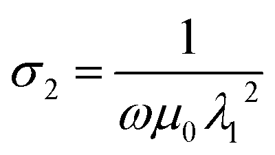
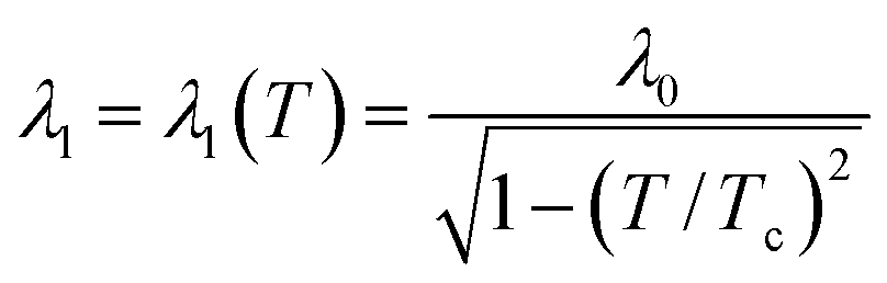
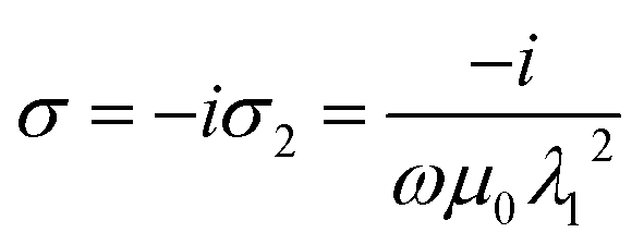
The standard two fluid model can be used to explain the frequency dependence of the permittivity of the superconductor material.73 So, the form of complex conductivity can be used to express the electromagnetic response of a superconductor as σ = σ1 − iσ2, where σ1 and σ2 represent the losses caused by regular electrons and super-electrons, respectively. The imaginary portion is written as74
 | (1) |
 | (2) |
 | (3) |
Therefore, the permittivity of the superconductor can be described as
 | (4) |
As illustrated in Fig. 1A, we mimic (imitate) the HMM layer with a subwavelength single-material semiconductor multilayer comprised of alternating undoped and doped InAs layers. (CD)8 refers to the subwavelength single-material semiconductor multilayer, where C represents the undoped InAs layer with the relative permittivity ε = nC2 = 3.52 (ref. 77) and D depicts the silicon-doped InAs(Si:InAs) layer with the relative permittivity D. The Drude model78 can be used to determine the relative permittivity of the Si:InAs layer.
 | (5) |
| εBx = pεC + (1 − p)εD | (6) |
 | (7) |
 | (8) |
 | (9) |
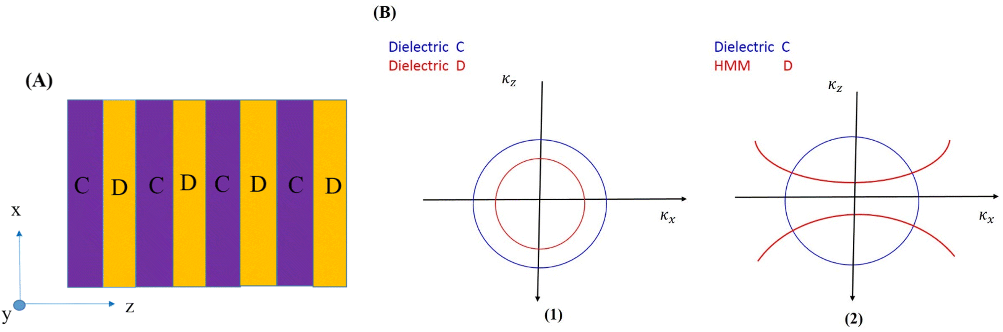 | ||
| Fig. 1 (A) Schematic of the subwavelength multilayer (CD)8 made of undoped InAs and silicon-doped InAs, those layers mimic (imitated) single-material semiconductor HMM layer. (B) Diagram of the dielectric and HMM iso-frequency curves under TM polarization. | ||
κ0 = ω/c denotes the wave vector in vacuum.
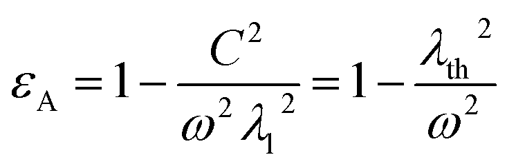
Furthermore, the iso-frequency curves of the PC media can be used to describe the process. The permittivity of the dielectric layers A and B is defined as εA and εB, respectively. The iso-frequency curves are shown in Fig. 1B(1). As the incident angle of light increases, the wave vector components κAz and κBz immediately decrease, whereas the horizontal component κx of the incident wave vector increases. Therefore, we consider a PC [AB]N with HMMs, where medium A is a conventional dielectric material and medium B is an HMM. The iso-frequency curves for layers A and B are shown in Fig. 1B(2). It was discovered that as κx increased, κBz increased in layer B while κAz reduced in layer A. The shifting performance of the band edge in the PC changes as the incident angle increases due to a phase variation compensating effect in the unit cell made up of the HMM and dielectric layers.80,81
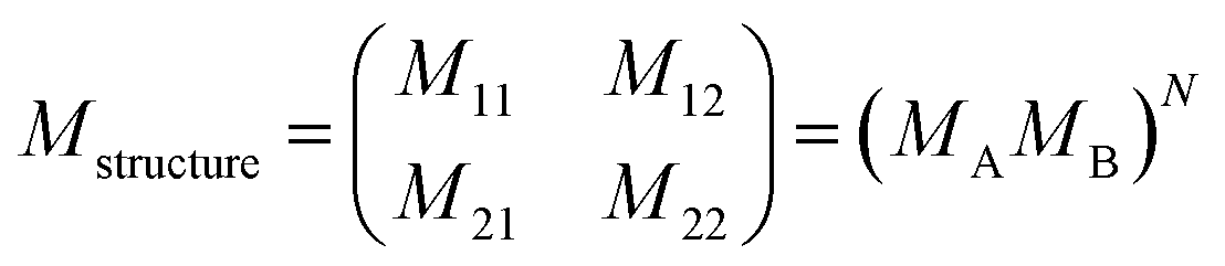
We offer a quick introduction of the characteristic matrix method that used to investigate the numerical findings. This approach is used to describe the interaction of incident electromagnetic waves with macroscopic material.82 The one-dimensional quasi-periodic PCs are made up of layers of superconductor material layered with HMM in the Fibonacci sequence. The superconductor layer is denoted by the sign (A), whereas the HMM layer is denoted by the symbol (B). The complete structure is then submerged in air. As a result, the Fibonacci sequence required to construct our design can be derived as Fj+1 = Fj + Fj−1. As a result, the Fibonacci sequence employed to construct our design is j ≥ 1 with F0 = {B} and F1={A}, resulting in F2 = F1F0 = {AB}, F2 = F2F1 = {ABA} and so on.36 The schematic illustration of the 1D quasi-periodic PCs based on the Fibonacci type of F7 is shown in Fig. 2. This illustration was made to show how our quasi-periodic PCs interact with the incident electromagnetic waves. The distinctive matrix method was used to explain such interactions.83–85
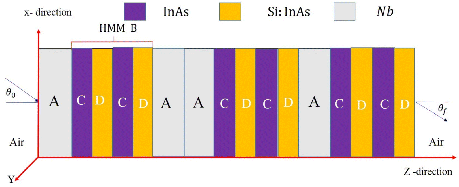 | ||
| Fig. 2 Schematic diagram of quasi-periodic PCs of F7 that configured as [Nb/(InAs/Si:InAs)8]. | ||
The response of Electromagnetic Waves (EMWs) through use of PCs was simply investigated using the transfer matrix method.86,87 To specify our design, we used the matrix equation below.
 | (10) |
MA and MB are the characteristic matrices for the superconductor layer (layer A) and the HMM layer (layer B), respectively, where:
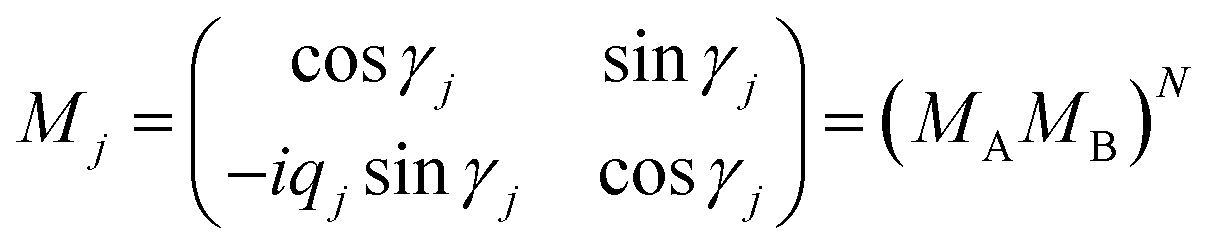 | (11) |
 | (12) |
 | (13) |
The transmittance can then be written as follows:
 | (14) |
3. Results and discussion
On the basis of the theoretical model described in the previous section, we now present the numerical results of our structure. We show the transmittance properties of one-dimensional quasi-periodic PCs across a wide range of incident electromagnetic wave wavelengths at normal incidence. Our results for the case of F7 are investigated, and the range is expanded from 800 to 2600 nm. The framework of our findings is based on the effect of superconductor material and HMM characteristics on the transmittance characteristics of Fibonacci-based structures. Thus, we set the thicknesses of the superconductor layer Niobium (Nb) and the single-material HMM layer to be dA = 30 nm and dB = 80 nm, respectively. A subwavelength InAs/Si:InAs multilayer (CD)s mimics the single-material HMM. The undoped InAs layer has a filling ratio of p = 0.5, where, the thickness InAs and the thickness of Si:InAs are dC = dD = 5![[thin space (1/6-em)]](https://www.rsc.org/images/entities/char_2009.gif) nm and periodicity of HMM s = 8 can be obtained. The HMM layer unit cell thickness is only 10 nm (approximately 0.031 times the designed Bragg wavelength), ensuring the accuracy of the effective medium theory.88 The optical properties of the proposed design have been demonstrated in the following sections based on the prior analysis. Meanwhile, we introduced the permittivity of superconductor material and HMM. We studied the transmittance characteristic of quasi-periodic PC containing HMM at different incident angle of EMW for TM polarization. We showed how the thickness of the Nb layer d1 and the periodicity of HMM affect the suggested PCs transmittance characteristics. Moreover, we studied the effect of the operating temperature and the filling ratio of InAs in our structure. Additionally, the transmittance properties of the designed quasi-periodic PC have been used to demonstrate the type of Fibonacci and the type of quasi-sequences.
nm and periodicity of HMM s = 8 can be obtained. The HMM layer unit cell thickness is only 10 nm (approximately 0.031 times the designed Bragg wavelength), ensuring the accuracy of the effective medium theory.88 The optical properties of the proposed design have been demonstrated in the following sections based on the prior analysis. Meanwhile, we introduced the permittivity of superconductor material and HMM. We studied the transmittance characteristic of quasi-periodic PC containing HMM at different incident angle of EMW for TM polarization. We showed how the thickness of the Nb layer d1 and the periodicity of HMM affect the suggested PCs transmittance characteristics. Moreover, we studied the effect of the operating temperature and the filling ratio of InAs in our structure. Additionally, the transmittance properties of the designed quasi-periodic PC have been used to demonstrate the type of Fibonacci and the type of quasi-sequences.
Fig. 3 indicated the effect of the operating temperature on the permittivity of the superconductor material through the wavelength range from 800 to 2600 nm. Both the wavelength of incident radiation and the operating temperature have a significant impact on the permittivity. In Fig. 3, we observed that the superconductor permittivity is increased by increasing the operating temperature as 4.2 K, 6 K and 8 K according to eqn (1) and (2). The value of the London penetration depth varies as the operating temperature increases, which have an effect on the permittivity of the superconductor layer. Then, the permittivity decreases with increasing the wavelength of the incident radiation where the permittivity has negative values for all range of wavelengths.
 | ||
| Fig. 3 The relationship between the wavelength of the incident electromagnetic waves and the Nb permittivity at various operating temperatures. | ||
Fig. 4 gives the response of the effective relative permittivity of the subwavelength InAs/Si:InAs multilayer (CD)8 through the wavelength range from 800 nm to 2600 nm. Eqn (6) and (7) could be used to quickly clarify such an effect. Wherein, at changing the filling ratio, the permittivity of HMM material along the x and z components change. This occurs as a result of an increase in the filling ratio of InAs. As a result, the permittivity of HMM material along the x and z components become pronounced. This figure led us to the concluding that the real Re(εBx) and the real Re(εBz) are changing with changing the filling ratio as shown in Fig. 4A and C, respectively. Wherein both of them are increasing with changing the filling ratio of InAs values as p = 0.35, p = 0.55, and p = 0.75. We observe that as the wavelength increases, the real Re(εBx) and Re(εBz) are essentially decrease. Fig. 4B and D depict how the imaginary Img(εBx) and Img(εBz) tends to zero where they independent of the incident radiation wavelength ranges.
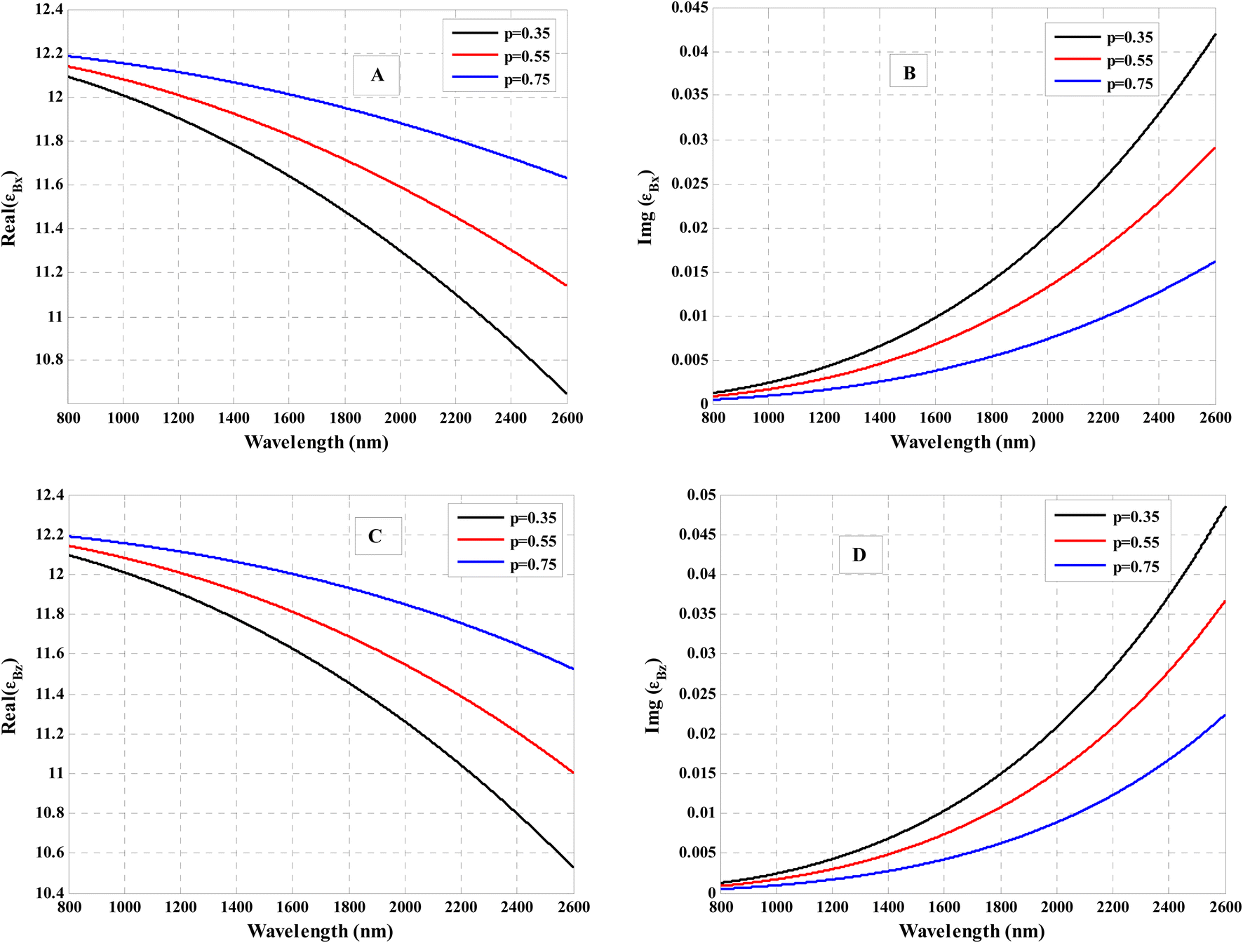 | ||
| Fig. 4 The response of the real and imaginary parts of the permittivity tensor of the subwavelength InAs/Si:InAs multilayer (CD)8 with the wavelength of the incident electromagnetic waves at various filling ratio of InAs where (A) Re(εBx), (B) Img(εBx), (C) Re(εBz) and (D) Img(εBz). | ||
Here, we investigate the transmittance spectra (TM polarization) of the proposed quasi-periodic photonic crystal [A(CD)8] for the case of F7 at different incident angles of 0°, 30°, 60°, and 75° by using the transfer matrix method89 as shown in Fig. 5. At normal incidence, multi resonance peaks have formed NIR region. Moreover, the intensity of their peaks are different. As demonstrated in Fig. 5, there is a resonance peak has a fixed position (called angle insensitive resonance peak). Other peaks have slightly blue and red shift with increasing the incident angle from 0° to 75° while their intensity are decreased. For example, the resonance peak at 1562 nm unaffected for its position but its intensity decreased from 0.54 to 0.49, to 0.43 and 0.33 when the incident angles changes of 0°, 30°, 60°, and 75° respectively. It is important to note that the insensitivity in this peak occur according to Fig. 1B(2) where the phase-variation compensation condition must be satisfied for  to be obtained,90 as shown in this equations
| Φ(λ,θ) = κAz(λ,θ)dA + κBz(λ,θ)dB | (15) |
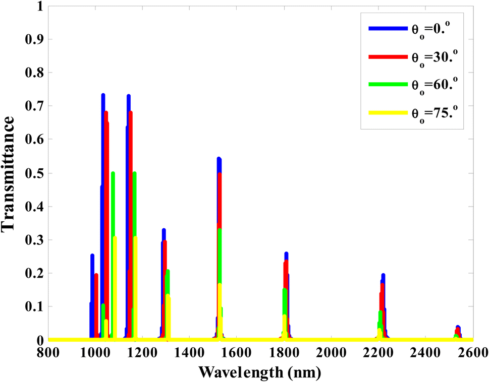 | ||
| Fig. 5 The transmittance spectra (TM polarization) of the designed quasi-periodic photonic crystal [A(CD)8] at various incident angles. | ||
Since ∂κBz/∂θ > 0 and ∂κAz/∂θ < 0
 | (16) |
Additionally, slightly blue shift occurs for the resonance peaks higher than the wavelength of 1562 nm and red shift occurs for the resonance peaks less than 1562 nm due to different values of the phase-variation compensation that may be more or less than the value of ∂κBz/∂θ. The slightly blue and red shift do not effect on the feasibilities of the design as it not reached to lower wavelengths, so these shifts cannot limit the fabrication of such design.
In addition, Fig. 5 present the intensity of transmittance for their resonance peaks in this wavelength range have significantly decreased. Eqn (13) and (14) show how transmission and incident angle are related. We discovered that as the angle of incidence increased, the transmission decreased. This result may be used as combination of pass bands and stop bands filter.
In this section, we show how certain parameters affect the transmittance characteristics of the suggested Fibonacci-based structure. This study will be done at constant operating (T = 4 K) temperature and filling ratio of InAs (p = 0.5). Fig. 6 depicts the transmittance properties of the structure at various thicknesses of superconductor (Nb) material. The resonance peaks are significantly affected as the thickness increases from 30 to 40, 50, and 60 nm, particularly NIR region, as shown in Fig. 6b–d, respectively. From Fig. 6, we found that the number of resonance peaks (8) becomes constant but the intensity of the transmittance decreases. Also, there is a definite shift towards the higher wavelengths in the range (800–1600 nm) while there is a shift towards the lower wavelengths in the range (1600–2600 nm). Wherein, the resonance peak at 1600 nm not shifted. Furthermore, using the following equation, this shift to the higher wavelengths as thickness increases can be explained:91
|
φi = 2πnidicos(θi)/λ
| (17) |
 .92,93 In this equation, ns represents the superelectrons, q gives the charge, m is the charge carriers mass, and μ0 denotes the permeability of the free space. Since the London penetration depth decreases, it suggests that the magnetic field of the incident electromagnetic wave has less penetration inside the superconductor layer. As a result, the intensity of the transmission of the resonance peaks decreases.
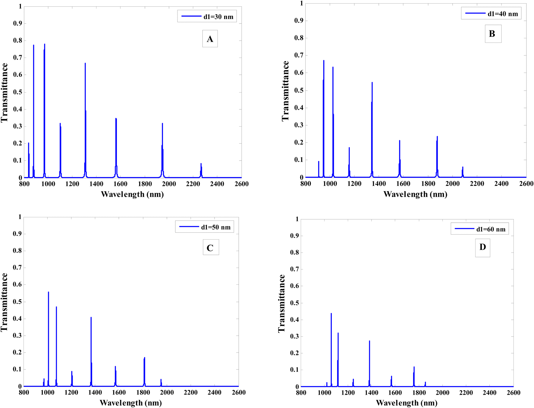 | ||
| Fig. 6 The transmittance spectra (TM polarization) of the designed quasi-periodic photonic crystal [A(CD)8] at various thickness of layer A (Nb) where (A) d1 = 30 nm, (B) d1 = 40 nm, (C) d1 = 50 nm and (D) d1 = 60 nm. | ||
In the following study, we investigate the effect of the number of periods of the HMM layer inside the suggested structure on the transmittance properties. As the number of period is increased, we noticed a difference in the number of resonance peaks, as shown in Fig. 7. The periodic number of HMM S = 2 results in two resonance peaks, as shown in Fig. 7A. Moreover, with increasing S = 4, 6 and 8 as seen in Fig. 7B–D, the number of resonance peaks increased until 8 resonance peaks with different intensity as shown in Fig. 7D. Increasing the HMM periodicity means increasing the thickness of this layer. Therefore, as the HMM layer thickness increases, different resonance peaks form at lower wavelengths, and the number of resonance peaks increases, which can be useful in some applications as a pass band and stop band filter. As a result, we can choose S = 8 as the optimization value of HMM periodicity.
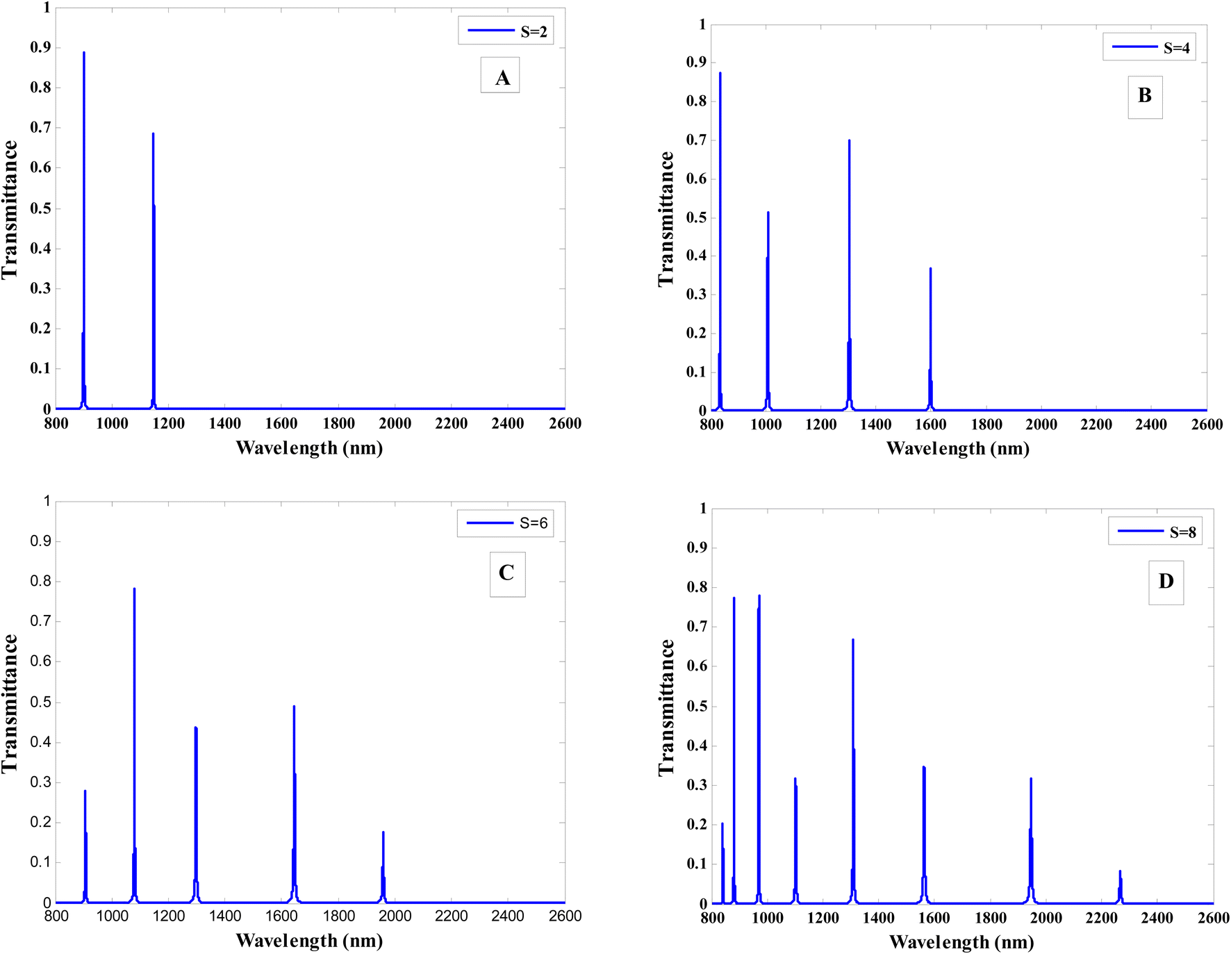 | ||
| Fig. 7 Transmittance spectra (TM polarization) of the quasi-periodic photonic crystal design [A(CD)8] at different periods in HMM layer (CD)S where (A) S = 2, (B) S = 4, (C) S = 6 and (D) S = 8. | ||
The study that follows will look into the effect of operating temperature on the transmittance. The theoretical model shows a clear relationship between the permittivity of such superconducting material and the operating temperature. As a result, there is a substantial different in the transmission spectra due to changes in operating temperature as shown in Fig. 8. The results show definitively that the number and location of the resonance peaks significantly change as the operating temperature of the superconductor material increases. As shown in Fig. 8A, the number, the position, and the amplitude are almost unaffected by variations in operating temperature at low values of the operating temperature, particularly for T < 4 K. For further increase in the temperature, the resonance peaks shifts to higher wavelengths as shown in Fig. 8C and D. In Fig. 8D, the number of resonance begin to decrease with increasing operating temperature to T = 8 K, because the number of super electrons has decreased relative to the number of normal electrons.94 Fig. 7 shows our observation that as the temperature of the SC layer increases, the intensity of the transmission of the resonance peaks increases. Eqn (2) provides an explanation for this behaviour. It is clear from this equation that the LPD λl increases with increasing the temperature. Since the London penetration depth increases, it indicates that the magnetic field of the incident electromagnetic wave has more penetration inside the superconductor layer. As a result, the intensity of the transmission of the resonance peaks increases.
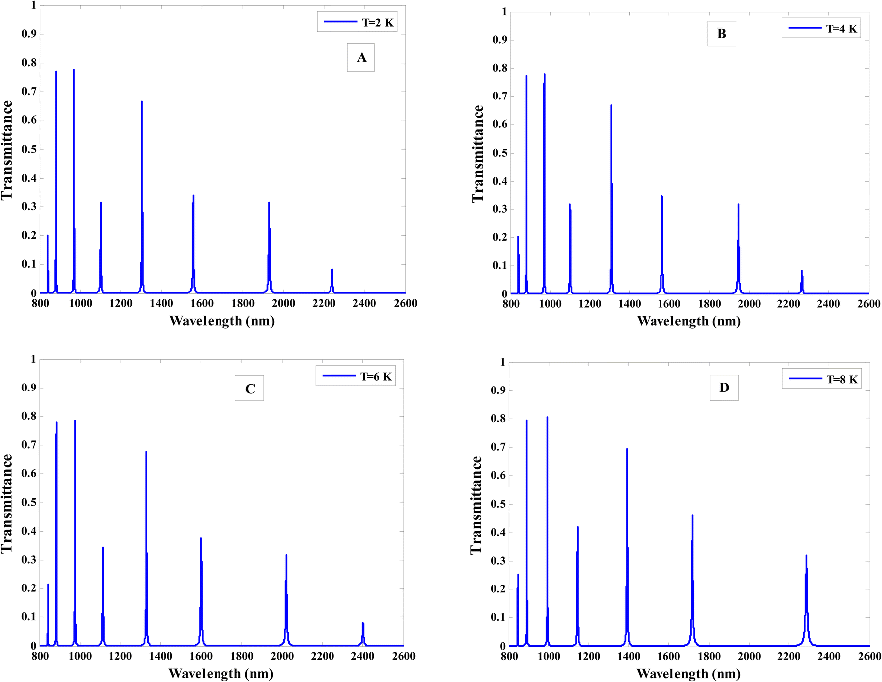 | ||
| Fig. 8 Transmittance spectra (TM polarization) of the designed quasi-periodic photonic crystal [A(CD)8] at different operating temperature of Nb layer where (A) T = 2 K, (B) T = 4 K, (C) T = 6 K and (D) T = 8 K. | ||
We investigate in Fig. 9 the dependence of the transmittance spectra on the threshold frequency of superconductor material. For using of Gallium (Ga) of Tc = 1.09 K and λl = 120 nm (ref. 95) in our design, Fig. 9A shows the appearance of 7 resonance peaks in all range of wavelength with highly different amplitudes. For substituting Nb of Tc = 9.2 K and, λl = 85.7 nm (ref. 96), there are 8 resonance peaks which are observed NIR until 2250 nm as shown in Fig. 9B. Moreover, the position and the intensity of this resonance peaks different that in case of Ga. The positions of resonance peaks shift to lower wavelengths where the intensity of resonance peaks are decreased. As Nb is replaced with vanadium silicide (V3Si) with Tc = 17.1 K and, λl = 70 nm (ref. 95), the resonance peaks shifts to lower wavelengths until reached to 1960 nm which are observed in NIR region. In addition to, the intensity of their resonance peaks is slightly decreased as seen in Fig. 9C. The position and intensity of the resonance peaks with changing the threshold frequency of the superconductor material. Finally, in the case of vanadium (V) (Tc = 5.3 K and λl = 39.8 nm),95 the resonance peaks extended from 800 nm to 1330 nm NIR range and their intensity are more decreased as shown in Fig. 9D.
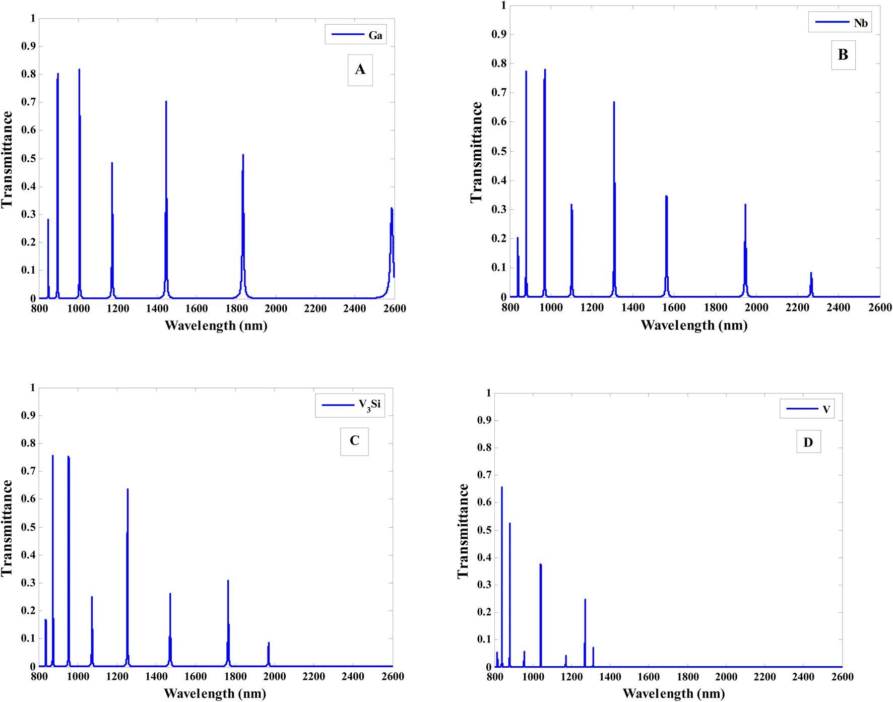 | ||
| Fig. 9 The transmittance spectra (TM polarization) of the quasi-periodic photonic crystal design [A(CD)8] at various types of the superconductor layer where (A) Ga with (Tc = 1.09 K and λ1 = 120 nm), (B) Nb with (Tc = 9.2 K and λ1 = 85.7 nm), (C) V3Si with (Tc = 17.1 K and λ1 = 70 nm) and (D) V with (Tc = 5.3 K and λ1 = 39.8 nm). | ||
Then, as shown in Fig. 10, we discuss the influence of the number of sequences on the transmittance response of our structure. The transmittance properties for the situation of F7 are studied in Fig. 10A. The figure shows the appearance of resonance peaks with different intensity. According to Fig. 10B and C, respectively, the number of resonance peaks starts to increase as the sequence number rises to F9 and F11, especially through the low wavelengths region. Moreover, the intensity of resonance peaks is decreased as comparable with the case of F7. In this case, increasing the sequence number results in more forms of periodicity that could be useful in tuning the resonance peaks.
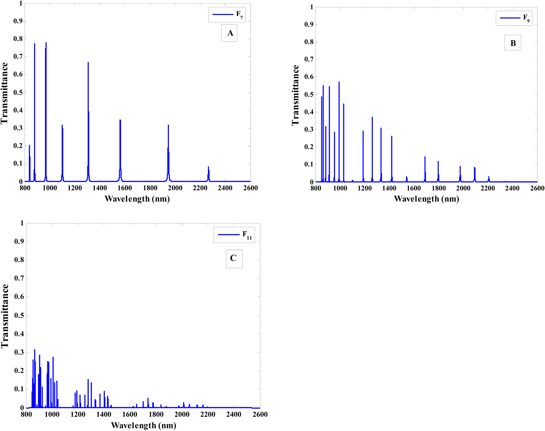 | ||
| Fig. 10 The transmittance spectra (TM polarization) of the designed quasi-periodic photonic crystal [A(CD)8] at various the sequence number for, (A) F7, (B) F9 and (C) F11. | ||
Finally, as shown in Fig. 11, we have studied the effect of using the various sequences. This figure shows transmittance in the cases of the seventh Fibonacci number, the fifth Thue–Morse number, and the fifth period doubling number. The most basic form of the Thue–Morse sequence is defined by the nested relations Tn = Tn−1Tn−1+ and Tn+ = Tn−1+Tn−1 for (n ≥ 1) with T0 = A, T0+ = B. This sequence can also be constructed using the inflation rules A → AB and B → BA. The Thue–Morse generations are97,98 T0 = A; T1 = AB; T2 = ABBA; T3 = ABBABAAB; etc. On the other hand, the double period sequence is obtained by Dn = Dn−1Dn−1+ and Dn+ = Dn−1+Dn−1 for (n ≥ 1) with D0 = A, D0+ = B. In addition to that, the double period sequence remains unchanged under the transitions A → AB and B → AA. The double-period generations are98,99 D0 = A; D1 = AB; D2 = ABAA; D3 = ABAAABAB; etc. Fig. 11B shows how the resonance peaks mostly follow a different path for Thue–Morse than for Fibonacci. Here, the intensity of resonance peaks decrease and their position becomes different. In the case of period doubling, it almost follows the same procedure as Thue–Morse, as shown in Fig. 11C. However, the intensity some resonance peaks increase and some other more decreased in comparable with the case of Thue–Morse sequence.
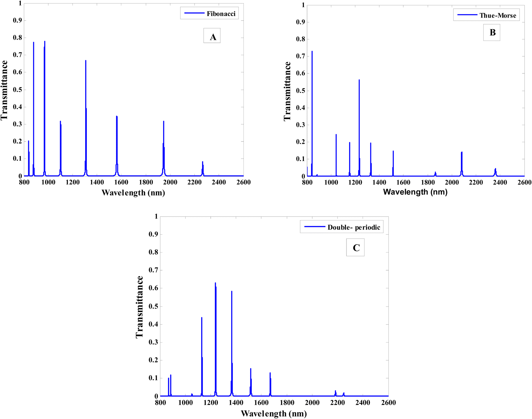 | ||
| Fig. 11 The transmittance spectra (TM polarization) of the designed quasi-periodic photonic crystal [A(CD)8] at different type of sequence for, (A) Fibonacci sequence, (B) Thue–Morse sequence and (C) the period doubling sequence. | ||
4. Fabrication feasibility and experimental tolerance
We present in this section the fabrication feasibility regarding our designed one-dimensional quasi-periodic PC, which consists of superconductor (Nb) and HMM based on the Fibonacci sequence, which can be fabricated through several steps. The fabrication of Nb layer, highly doped InAs and undoped InAs layer is already occurred with high quality. There are some examples of fabrication ultrathin films of Nb through a combined structure and electronic analysis of niobium ultrathin films (from 2 to 10 nm) formed in an ultra-high vacuum on atomically flat R-plane sapphire wafers.100,101 Thinner than 3.3 nm, or almost the first measurement of a superconducting state, hetero-epitaxy is not possible, as shown by the textured polycrystalline morphology of the thinnest films. One monolayer (ML) is typically the thickness range over which the superconducting critical temperature rises. Standard nanofabrication methods can be applied to the thinnest superconducting sample (3 nm/9 ML), which has a compensate critical temperature above 4.2 K, to produce air- and time-stable superconducting nanostructures that are helpful for quantum devices.By multilayer sequential sparking on niobium at substrate temperatures ranging from room temperature to 250 °C, Md Nizam Sayeed et al. actually described the fabrication of niobium tin (Nb3Sn) films.102 They examined the resistivity of the superconducting films from room temperature to below the superconducting critical temperature Tc. The multilayers were deposited at room temperature, yielding a film Tc of 17.76 K. The films Tc of 17.58 K are produced when the deposition temperature is increased to 250 °C, and voids were significantly reduced.
The synthesis of high-quality materials is supported by manufactured InAs/GaSb (like our structure), which has a strong optical signal at room temperature. The current–voltage characteristics of manufactured InAs/GaSb p-i-n tunnel diodes when measured at 77 K and 290 K showed two bias-dependent transport mechanisms.103 Also, there is no errors can be expected as layered semiconductor hyperbolic metamaterials already fabricated for the mid-infrared and are grown by molecular beam epitaxy (MBE) using a single material system, doped and undoped InAs.104 This material of choice has two benefits: it can be grown by MBE relatively easily, and it has the shortest plasma wavelength of any III/V material. Additionally, the capability of tuning across the mid-infrared spectrum, adjusting the doping level in the metal layers, and controlling the onset of HMM behaviour.
On the other hand, the fabrication tolerance is a crucial variable that can have a significant impact on how well this structure performs in a variety of applications. A range of suitable variations in the layer's thickness is usually employed to define the allowed tolerance in the thickness for a proposed structure. Tight tolerances in the thickness are occurred usually in nano photonics, where such a tolerance of the thin film can significantly affect the performance of optical devices. The required specifications for the film and the specific application determine the acceptable tolerances.
Typically, the expected tolerances for the thickness of any film are expressed as a range, like ±5% of the nominal thickness. If the film thickness is outside of this range, it might not be appropriate for the use that was intended. In this regard, Fig. 12 makes clear how tolerance affects both the intensity of the transmittance and the shift in the resonant peaks. Here, two different fabrication tolerance values ±5% and ±10% are taken into account. The investigated numerical findings show that the resonance peaks shift to higher wavelengths and the intensity of the transmittance slightly decreased gradually as the fabrication error receives +5% and +10% as showed in Fig. 12B and D. On the other hand, the resonance peaks shift to lower wavelengths and the intensity of the transmittance slightly increased due to a fabrication tolerance of −5% and −10% as showed in Fig. 12C and E. For further increase in the fabrication tolerance to +10% or −10%, the number of resonance peaks and the intensity of the transmittance may decreased. Therefore, a tolerance value of ±5% is considered an acceptable tolerance value and it was proved that does not possess high perturbations on the performance of this structure. Therefore, the proposed design is stable against the small variations in the thickness.
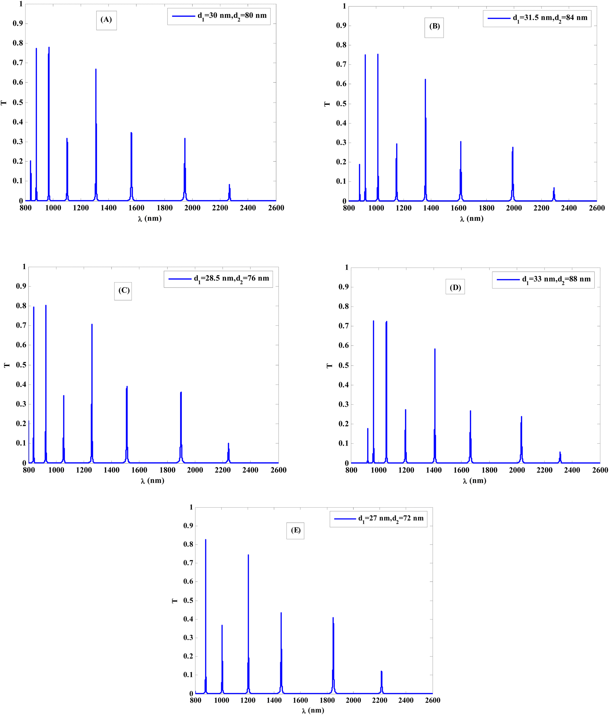 | ||
| Fig. 12 The transmittance spectra (TM polarization) under the effect of fabrication tolerance (A) normal thickness, (B) thickness +5%, (C) thickness −5%, (D) thickness +10% and (E) thickness −10%. | ||
5. Conclusion
In conclusion, we theoretically examined the NIR transmittance characteristics of a one-dimensional quasi-periodic PC. The proposed structure is made up of a superconductor (Nb) and HMM based on the Fibonacci sequence. In our design, the properties of resonance peaks with angle stability are theoretically calculated by using the characteristic matrix model and the effective medium theory. The effects of thickness, operating temperature, and the type of superconductor layer on the properties of the resonance peaks are studied. The permittivity of (Nb) at various operating temperatures and the permittivity of HMM at different filling ratios are also investigated. Moreover, the number of Fibonacci sequences and type of each sequence have proved to sustain a pronounced effect on the number and position of the resonance peaks. The proposed structure has the ability to enhance the quality and performance of the preceding fields and can be used as an optical pass/stop band filter for NIR applications.Conflicts of interest
There are no conflicts to declare.References
- E. Yablonovitch, Inhibited Spontaneous Emission in Solid-State Physics and Electronics, Phys. Rev. Lett., 1987, 58, 2059–2062 CrossRef CAS PubMed.
- S. John, Strong localization of photons in certain disordered dielectric superlattices, Phys. Rev. Lett., 1987, 58, 2486 CrossRef CAS PubMed.
- H. A. Elsayed, A multi-channel optical filter by means of one dimensional n doped semiconductor dielectric photonic crystals, Mater. Chem. Phys., 2018, 216, 191–196, DOI:10.1016/j.matchemphys.2018.06.016.
- A. H. Aly and H. A. Elsayed, Defect mode properties in a one-dimensional photonic crystal, Physica B Condens. Matter, 2012, 407, 120–125, DOI:10.1016/j.physb.2011.09.137.
- H. A. Elsayed, Photonic Band Gaps Properties of Two-Dimensional Ternary Superconductor Photonic Crystals, Surf. Rev. Lett., 2019, 26(3), 1850152, DOI:10.1142/S0218625X18501524.
- A. H. Aly, W. Sabra and H. A. Elsayed, Dielectric and Superconducting Photonic Crystals, J. Supercond. Nov. Magnetism, 2013, 26, 553–560, DOI:10.1007/s10948-012-1791-y.
- A. H. Aly, D. Mohamed, H. A. Elsayed and A. Mehaney, Fano Resonance by Means of the One-Dimensional Superconductor Photonic Crystals, J. Supercond. Novel Magn., 2018, 31, 3827–3833, DOI:10.1007/s10948-018-4660-5.
- Mohamed, H. A. ElSayed, A. Mehaney, A. H. Aly and W. Sabra, The transmissivity of one-dimensional photonic crystals comprisingthree phases nanocomposite layer for optical switching purposes, Phys. Scr., 2021, 96, 115504, DOI:10.1088/1402-4896/ac15c6.
- A. H. Aly and W. Sabra, Superconductor-Semiconductor Metamaterial Photonic Crystals, J. Supercond. Nov. Magn., 2016, 29, 1981–1986 CrossRef CAS.
- C. Malek, A. H. Aly, S. Alamri and W. Sabra, Tunable PBGs with a cutoff frequency feature in Fibonacci quasi-periodic designs containing a superconductor material at THz region, Phys. Scr., 2021, 96(10), 105501–105510 CrossRef.
- W. Sabra, H. A. Elsayed, A. Mehaney and A. H. Aly, Numerical optimization of 1D superconductor photonic crystals pressure sensor for low temperatures applications, Solid State Commun., 2022, 343, 15 CrossRef.
- C. Malek, M. Al-Dossari, S. K. Awasthi, Z. S. Matar, N. S. Abd El-Gawaad, W. Sabra and A. H. Aly, Employing the Defective Photonic Crystal Composed of Nanocomposite Superconducting Material in Detection of Cancerous Brain Tumors Biosensor: Computational Study, Crystals, 2022, 12(4), 540 CrossRef CAS.
- A. H. Aly, S. K. Awasthi, A. M. Mohamed, Z. S. Matar, M. A. Mohaseb, M. Al-Dossari, M. T. Tammam, Z. A. Zaky, A. F. Amin and W. Sabra, Detection of Reproductive Hormones in Females by Using 1D Photonic Crystal-Based Simple Reconfigurable Biosensing Design, Crystals, 2021, 11, 1533 CrossRef CAS.
- H. A. Elsayed, Quasiperiodic photonic crystals for filtering purpose by means of the n doped semiconductor material, Phys. Scr., 2020, 95, 065504, DOI:10.1088/1402-4896/ab7f4a.
- Mohamed, W. Sabra, A. H. Aly, M. Mobarak and A. S. Shalaby, A defective one-dimensional superconducting photonic crystal design for the generation of the Fano resonance feature, Phys. Scr., 2020, 95, 115503, DOI:10.1088/1402-4896/abbd69.
- H. Aly, W. Sabra and H. A. Elsayed, Cutoff frequency in metamaterials photonic crystals within Terahertz frequencies, Int. J. Mod. Phys. B, 2017, 31, 1750123, DOI:10.1142/S0217979217501235.
- J. Barvestani, E. Rezaei and A. S. Vala, Tunability of waveguide modes in twodimensional photonic crystals based on superconducting materials, Opt. Commun., 2013, 297, 74–78, DOI:10.1016/j.optcom.2013.01.069.
- H. A. Elsayed, S. A. El-Naggar and A. H. Aly, Thermal properties and twodimensional photonic band gaps, J. Mod. Opt., 2014, 61, 385–389, DOI:10.1080/09500340.2014.887155.
- A. Mehaney, A. M. Ahmed, H. A. Elsayed, A. H. Aly and W. Sabra, Hydrostatic pressure effects for controlling the phononic band gap properties in a perfect phononic crystal, Opt. Quant. Electron., 2022, 54, 94 CrossRef CAS.
- H. A. Elsayed, A. Sharma, F. Segovia-Chaves and W. Sabra, Multi passbands filter for THz applications based on the one-dimensional photonic crystals heterostructure, Optik, 2021, 248, 168056 CrossRef CAS.
- A. H. Aly, H. A. Elsayed and H. S. Hamdy, The optical transmission characteristics in metallic photonic crystals, Mater. Chem. Phys., 2010, 124, 856–860, DOI:10.1016/j.matchemphys.2010.08.006.
- H. A. Elsayed, Transmittance properties of one dimensional ternary nanocomposite photonic crystals, Mater. Res. Express, 2018, 5, 036209, DOI:10.1088/2053-1591/aaaf79.
- R. H. Hadfield, Single-photon detectors for optical quantum information applications, Nat. Photonics, 2009, 3, 696–705, DOI:10.1038/nphoton.2009.230.
- H. Kong and H.-Y. Lee, Thermal darkening of one-dimensional photonic crystal containing tellurium suboxide, Opt. Mater., 2019, 88, 167–175, DOI:10.1016/j.optmat.2018.11.032.
- Y.-H. Chen, W.-H. Shi, L. Feng, X.-Y. Xu and M.-Y. Shang-Guan, Study on simultaneous sensing of gas concentration and temperature in one-dimensional photonic crystal, Superlatt. Microstr., 2019, 131, 53–58, DOI:10.1016/j.spmi.2019.05.033.
- H. A. Elsayed and A. H. Aly, Terahertz frequency superconductor-nanocomposite photonic band gap, Int. J. Mod. Phys. B, 2018, 32, 1850056, DOI:10.1142/S021797921850056X.
- S. R. Qutb, A. H. Aly and W. Sabra, Salinity and temperature detection for seawater based on a 1D-defective photonic crystal material, Int. J. Mod. Phys. B, 2021, 2150012 CrossRef CAS.
- S. Razi and F. Ghasemi, Tunable graphene based one dimensional photonic crystal with applications in terahertz optical integrated circuits, Physica B Condens. Matter, 2019, 566, 77–85, DOI:10.1016/j.physb.2019.05.001.
- O. A. Abd El-Aziz, H. A. Elsayed and M. I. Sayed, One-dimensional defective photonic crystals for the sensing and detection of protein, Appl. Opt., 2019, 58, 8309–8315, DOI:10.1364/AO.58.008309.
- H. A. Elsayed and A. Mehaney, A new method for glucose detection using the one dimensional defective photonic crystals, Mater. Res. Express, 2019, 6, 036201, DOI:10.1088/2053-1591/aaf3da.
- S. Mokkapati and K. R. Catchpole, Nanophotonic light trapping in solar cells, J. Appl. Phys., 2012, 112, 101101, DOI:10.1063/1.4747795.
- Y. Wu, J. Lu, M. Li, J. Yuan, P. Wu, X. Chang, C. Liu and X. Wang, Bismuth silicate photocatalysts with enhanced light harvesting efficiency by photonic crystal, J. Alloys Compd., 2019, 810, 151839, DOI:10.1016/j.jallcom.2019.151839.
- Q. Li, S. Zhou, T. Zhang, B. Zheng and H. Tang, Bioinspired sensor chip for detection of miRNA-21 based on photonic crystals assisted cyclic enzymatic amplification method, Biosens. Bioelectron., 2020 DOI:10.1016/j.bios.2019.111866.
- X. Qiu, W. Chen, Y. Luo, Y. Wang, Y. Wang and H. Guo, Highly sensitive α- amanitin sensor based on molecularly imprinted photonic crystals, Anal. Chim. Acta, 2020, 1093, 142–149, DOI:10.1016/j.aca.2019.09.066.
- R. Dalmis, O. Y. Keskin, N. Funda Ak Azem and I. Birlik, A new onedimensional photonic crystal combination of TiO2/CuO for structural color applications, Ceram. Int., 2019, 45, 21333–21340, DOI:10.1016/j.ceramint.2019.07.119.
- H. F. Zhang, J. P. Zhen and W. P. He, Omnidirectional photonic band gaps enhanced by Fibonacci quasi-periodic one-dimensional ternary plasma photonic crystals, Optik, 2013, 124(20), 4182–4187, DOI:10.1016/j.ijleo.2012.12.047.
- H. A. Elsayed, Quasiperiodic photonic crystals for filtering purpose by means of the n doped semiconductor material, Phys. Scr., 2020, 109766, DOI:10.1088/1402-4896/ab7f4a.
- E. F. Silva, C. H. Costa, M. S. Vasconcelos and D. H. A. L. Anselmo, Transmission spectra in graphene-based octonacci one-dimensional photonic quasicrystals, Opt. Mater., 2019, 89, 623–629, DOI:10.1016/j.optmat.2018.06.031.
- Y. Trabelsi, N. B. Alia, A. Elhawil, R. Krishnamurthy, M. Kanzari, I. S. Amiri and P. Yupapin, Design of structural gigahertz multichanneled filter by using generalized Fibonacci superconducting photonic quasicrystals, Results Phys., 2019, 13, 102343, DOI:10.1016/j.rinp.2019.102343.
- M. Bellingeri, A. Chiasera, I. Kriegel and F. Scotognella, Optical properties of periodic, quasi-periodic, and disordered one-dimensional photonic structures, Opt. Mater., 2017, 72, 403–421, DOI:10.1016/j.optmat.2017.06.033.
- A. H. Aly, C. Malek and H. A. Elsayed, Transmittance properties of a quasi-periodic one-dimensional photonic crystals that incorporate nanocomposite material, Int. J. Mod. Phys. B, 2018, 32, 1850220, DOI:10.1142/S021797921850220X.
- W. Steurer and D. S. Widmer, Photonic and phononic quasicrystals, J. Phys. D: Appl. Phys., 2007, 40, R229, DOI:10.1088/0022-3727/40/13/R01.
- T. Fujiwara, M. Kohmoto and T. Tokihiro, Multifractal wave functions on a Fibonacci lattice, Phys. Rev. B: Condens. Matter Mater. Phys., 1989, 40, 7413, DOI:10.1103/PhysRevB.40.7413.
- H. A. Elsayed, S. A. El-Naggar and A. H. Aly, Two dimensional tunable photonic crystals and n doped semiconductor materials, Mater. Chem. Phys., 2015, 160, 221, DOI:10.1016/j.matchemphys.2015.04.027.
- A. H. Aly, H. A. Elsayed and H. S. Hamdy, Mater. Chem. Phys., 2010, 124, 856 CrossRef CAS.
- S. A. El-Naggar, H. A. Elsayed and A. H. Aly, J. Supercond. Nov. Magn., 2014, 27, 1615 CrossRef CAS.
- A. H. Aly, S. W. Ryu, H. T. Hsu and C. J. Wu, Mater. Chem. Phys., 2009, 113, 382 CrossRef CAS.
- A. H. Aly, J. Supercond. Nov. Magn., 2008, 21, 421 CrossRef CAS.
- S. Y. Xiao, T. T. Liu, L. Cheng, C. B. Zhou, X. Y. Jiang, Z. Li and C. Xu, J. Lightwave Technol., 2018, 37, 3290 Search PubMed.
- P. Alexander, I. Ivan, B. Pavel and K. Yuri, Nat. Photonics, 2013, 948 Search PubMed.
- V. P. Drachev, V. A. Podolskiy and A. V. Kildishev, Opt. Express, 2013, 21, 15048 CrossRef PubMed.
- A. M. DaSilva, Y. C. Chang, T. Norris and A. H. MacDonald, Phys. Rev. B, 2013, 88, 195411 CrossRef.
- C. Guclu, S. Campione and F. Capolino, Hyperbolic metamaterial as super absorber for scattered fields generated at its surface, Phys. Rev. B: Condens. Matter Mater. Phys., 2012, 8, 205130, DOI:10.1103/PhysRevB.86.205130.
- J. Zhou, A. F. Kapla, L. Chen and L. Guo, Experiment and Theory of the Broadband Absorption by a Tapered Hyperbolic Metamaterial Array, ACS Photonics, 2014, 1, 618–624, DOI:10.1021/ph5001007.
- I. Iorsh, I. Mukhin and I. Shadrivov, Phys. Rev. B: Condens. Matter Mater. Phys., 2012, 87, 486 Search PubMed.
- A. W. Zeng and B. Guo, Opt. Quant. Electron., 2017, 49(1), 200 CrossRef.
- M. Shoaei, M. K. Moravvej-Farshi and L. Yousefi, All-optical switching of nonlinear hyperbolic metamaterials in visible and near-infrared regions, J. Opt. Soc. Am. B, 2015, 32, 2358–2365, DOI:10.1364/JOSAB.32.002358.
- X. Zhou, X. Yin, T. Zhang, L. Chen and X. Li, Ultrabroad terahertz bandpass filter by hyperbolic metamaterial waveguide, Opt. Express, 2015, 23, 11657–11664, DOI:10.1364/OE.23.011657.
- Y. Shen, Y. Yan, A. N. Brigeman, H. Kim and N. C. Giebink, Efficient Upper-Excited State Fluorescence in an Organic Hyperbolic Metamaterial, Nano Lett., 2018, 18, 1693–1698, DOI:10.1021/acs.nanolett.7b04738.
- J. Liu, G. V. Naik, S. Ishii, C. DeVault and A. Boltasseva, Optical absorption of hyperbolic metamaterial with stochastic surfaces, Opt. Express, 2014, 22, 8893–8901, DOI:10.1364/OE.22.008893.
- H. W. Dong, S. D. Zhao, Y. S. Wang and C. Zhang, Topology optimization of anisotropic broadband double-negative elastic metamaterials, Sci. Rep., 2017, 105, 54–80, DOI:10.1016/j.jmps.2017.04.009.
- Y. Sun, Z. Zheng, J. Cheng, G. Sun and G. Qiao, Highly efficient second harmonic generation in hyperbolic metamaterial slot waveguides with large phase matching tolerance, Opt. Express, 2015, 23, 6370–6378, DOI:10.1364/OE.23.006370.
- C. T. Riley, J. S. T. Smalley, J. R. J. Brodie, Y. Fainman, D. J. Sirbuly and Z. Liu, Proc. Natl. Acad. Sci. India, 2017, 114, 1264 CAS.
- M. A. Baqir and P. K. Choudhury, Design of Hyperbolic Metamaterial-Based Absorber Comprised of Ti Nanospheres, IEEE Photon. Technol. Lett., 2019, 31(10), 735–738, DOI:10.1109/LPT.2019.2906323.
- K. Maeno, B. R. Patel, T. Endo and K. Kerman, Angle-Sensitive Photonic Crystals for Simultaneous Detection and Photocatalytic Degradation of Hazardous Diazo Compounds, Micromachines, 2020, 11, 93, DOI:10.3390/mi11010093.
- C. Song, Y. Feng, G. Liu and J. Wang, Angle-Insensitive Color Filters Based on Multilayer Ultrathin-Film Structures, Plasmonics, 2019, 15, 255–261, DOI:10.1007/s11468-019-01028-2.
- X. K. Kong, S. B. Liu, H. F. Zhang, B. Bian and C. Chen, Phys. Plasmas, 2014, 21, 122310 CrossRef.
- J. Guo, S. Chen and S. Jiang, J. Mod. Opt., 2017, 65, 928 CrossRef.
- H. Tanaka, I. Takai, H. Fujikawa and H. J. Lizuka, J. Lightwave Technol., 2018, 36, 2517 CAS.
- Y. Ma, et al., Te electromagnetic wave modulation based on single-frequency refection in absorption with angle stability of hyperbolic metamaterials, J. Opt., 2020, 22, 095103, DOI:10.1088/2040-8986/aba586.
- C. Xue, Y. Ding, H. Jiang, Y. Li, Z. Wang, Y. Zhang and H. Chen, Phys. Rev. B, 2016, 93, 125310 CrossRef.
- D. Wei, C. Harris, C. C. Bomberger, J. Zhang, J. Zide and S. Law, Single-material semiconductor hyperbolic metamaterials, Opt. Express, 2016, 24, 8735–8745, DOI:10.1364/OE.24.008735.
- M. Born and E. Wolf, Principles of Optics, Cambridge, London, 1999 Search PubMed.
- T. Van Duzer and C. W. Turner, Principles of Superductive Devices and Circuits, Edward Arnold, London, 1981 Search PubMed.
- A. H. Aly, H.-T. Hsu, T.-J. Yang, C.-J. Wu and C. K. Hwangbo, J. Appl. Phys., 2009, 105, 083917 CrossRef.
- H. Aly, A. Aghajamali, H. ElSayed and M. Mohamed, Analysis of cutoff frequency in a one-dimensional superconductor-metamaterial photonic crystal, Physica C, 2016 DOI:10.1016/j.physc.2016.05.025.
- E. Palik, Handbook of Optical Constants of Solids, Academic, New York, 1998 Search PubMed.
- A. H. Aly and D. Mohamed, BSCCO/SrTiO3 One Dimensional Superconducting Photonic Crystal for Many Applications , J. Supercond. Novel Magn., 2015, 18, 1699–1703, DOI:10.1007/s10948-015-2993-x.
- A. Poddubny, I. Iorsh, P. Belov and Y. Kivshar, Hyperbolic metamaterials, Nat. Photonics, 2013, 7, 948–957, DOI:10.1038/nphoton.2013.243.
- F. Wu, G. Lu, C. Xue, H. Jiang, Z. Guo, M. Zheng, C. Chen, G. Du and H. Chen, Experimental demonstration of angle-independent gaps in one-dimensional photonic crystals containing layered hyperbolic metamaterials and dielectrics at visible wavelengths, Appl. Phys. Lett., 2018, 112(4), 041902, DOI:10.1063/1.5018070.
- F. Wu, G. Lu, Z. Guo, H. Jiang, C. Xue, M. Zheng, C. Chen, G. Du and H. Chen, Redshift gaps in one-dimensional photonic crystals containing hyperbolic metamaterials, Phys. Rev. Appl., 2018, 10(6), 064022, DOI:10.1103/PhysRevApplied.10.064022.
- H. A. Elsayed and M. M. Abadla, Transmission investigation of one-dimensional Fibonacci-based quasi-periodic photonic crystals including nanocomposite material and plasma, Phys. Scr., 2020, 95(3), 035504, DOI:10.1088/1402-4896/ab4c68.
- M. Born and E. Wolf, Principles of Optics, Cambridge, London, 1999 Search PubMed.
- W. Li-gang, L. Nian-hua, L. Qiang and Z. Shi-yao, Propagation of coherent and partially coherent pulses through one-dimensional photonic crystals, Phys. Rev. E, 2004, 70, 016601, DOI:10.1103/PhysRevE.70.016601.
- S. J. Orfanidis, Electromagnetic Waves and Antennas, Rutger University, 2008 Search PubMed.
- P. Yeh, Optical Waves in Layered Media, Wiley-Interscience, 2005 Search PubMed.
- S. Orfanidis, Electromagnetic Waves and Antennas, NJ Rutgers University, New Brunswick, 2008 Search PubMed.
- V. E. Babicheva, M. Y. Shalaginov, S. Ishii, A. Boltasseva and A. V. Kildishev, Long-range plasmonic waveguides with hyperbolic cladding, Opt. Express, 2015, 23, 9681, DOI:10.1364/OE.23.031109.
- P. Yeh, Optical Waves in Layered Media, Wiley, New York, 1988 Search PubMed.
- A. G. Mohamed, W. Sabra, M. Ahmed, A. H. Aly and H. A. Elsayed, Multiplication of photonic band gaps in one-dimensional photonic crystals by using hyperbolic metamaterial in IR range, Sci. Rep., 2023, 13, 324, DOI:10.1038/s41598-023-27550-2.
- H. A. Elsayed, F. A. Sayed and A. H. Aly, Graphene deposited liquid crystal and thermal sensitivity using photonic crystals, Phys. Scr., 2021, 96, 035503, DOI:10.1088/1402-4896/abdbf5.
- W. Buckel and R. Kleiner, Superconductivity fundamentals and applications Solid State Physics, New York, Wiley, 2004, ch 1 Search PubMed.
- A. H. Aly and W. Sabra, Effective surface impedance of a high temperature superconductor, Physica C, 2013, 495, 126–129 CrossRef CAS.
- A. H. Aly, H. A. Elsayed and S. A. El-Naggar, J. Mod. Opt., 2014, 61, 1064 CrossRef.
- T. Van Duzer and C. W. Turner, Principles of Superductive Devices and Circuits, Edward Arnold, London, 1981 Search PubMed.
- W. Buckel and R. Kleiner, Superconductivity: Fundamentals and Applications, VCH, Weinheim, 2004 Search PubMed.
- Q. Liu, S. Li, H. Chen, J. Li and Z. Fan, High-sensitivity plasmonic temperature sensor based on photonic crystal fiber coated with nanoscale gold film, Appl. Phys. Express, 2015, 8, 046701, DOI:10.7567/APEX.8.046701.
- B. K. Singh and P. C. Pandey, Influence of graded index materials on the photonic localization in one-dimensional quasi-periodic (Thue –Mosre and Double - Periodic) photonic crystals, Opt. Commun., 2014, 333, 84–91, DOI:10.1016/j.optcom.2014.07.043.
- E. L. Albuquerque and M. G. Cottam, Theory of elementary excitations in quasi-periodic structures, Phys. Rep., 2003, 376, 225–337, DOI:10.1016/S0370-1573(02)00559-8.
- C. Delacour, L. Ortega, M. Faucher, T. Crozes, T. Fournier, B. Pannetier and V. Bouchiat, Persistence of superconductivity in niobium ultrathin films grown on R-Plane Sapphire, Phys. Rev. B: Condens. Matter Mater. Phys., 2011, 83(14) DOI:10.1103/PhysRevB.83.144504.
- R. Espiau de Lamaestre, P. Odier, E. Bellet-Amalric, P. Cavalier, S. Pouget and J.-C. Villégier, High Quality Ultrathin NbN Layers On Sapphire for Superconducting Single Photon Detectors, J. Phys.: Conf. Ser., 2008, 97(1), 012046, DOI:10.1088/1742-6596/97/1/012046.
- Sayeed, U. Pudasaini, C. E. Reece, G. V. Eremeev and H. E. Elsayed-Ali, Effect of substrate temperature on the growth of Nb3Sn film on Nb by multilayer sputtering, Thin Solid Films, 2022, 763, 139569, DOI:10.1016/j.tsf.2022.139569.
- J.-S. Liu, M. B. Clavel, R. Pandey, S. Datta, M. Meeker, G. A. Khodaparast and M. K. Hudait, Growth and characterization of metamorphic InAs/GaSb tunnel heterojunction on GaAs by molecular beam epitaxy, J. Appl. Phys., 2016, 119, 244308, DOI:10.1063/1.4954794.
- D. Wei, C. Harris, C. C. Bomberger, J. Zhang, J. Zide and S. Law, Opt. Express, 2016, 24, 8735 CrossRef CAS PubMed.
| This journal is © The Royal Society of Chemistry 2023 |