DOI:
10.1039/D3RA01867A
(Paper)
RSC Adv., 2023,
13, 17968-17977
Semiconductor and topological phases in lateral heterostructures constructed from germanene and AsSb monolayers†
Received
22nd March 2023
, Accepted 23rd May 2023
First published on 13th June 2023
Abstract
Two-dimensional (2D) heterostructures have attracted a lot of attention due to their novel properties induced by the synergistic effects of the constituent building blocks. In this work, new lateral heterostructures (LHSs) formed by stitching germanene and AsSb monolayers are investigated. First-principles calculations assert the semimetal and semiconductor characters of 2D germanene and AsSb, respectively. The non-magnetic nature is preserved by forming LHSs along the armchair direction, where the band gap of the germanene monolayer can be increased to 0.87 eV. Meanwhile, magnetism may emerge in the zigzag-interline LHSs depending on the chemical composition. Such that, total magnetic moments up to 0.49 μB can be obtained, being produced mainly at the interfaces. The calculated band structures show either topological gap or gapless protected interface states, with quantum spin-valley Hall effects and Weyl semimetal characters. The results introduce new lateral heterostructures with novel electronic and magnetic properties, which can be controlled by the interline formation.
I. Introduction
Stimulated by the successful investigations and applications of graphene and its derivatives,1–4 a large variety of two-dimensional (2D) materials have been prepared in experiments and predicted by theoretical calculations.5–10 In comparison with their three-dimensional (3D) bulk counterparts, 2D materials usually exhibit unique properties that make them suitable for diverse applications.11–14 In addition, different feature-rich characteristics can be obtained by means of surface modification,15,16 doping,17,18 application of external strain and electric field,19–21 and formation of heterostructures. Between them, 2D van der Waals vertical heterostructures (VHSs) – two vertically stacked 2D materials – have been commonly investigated, including ones formed by graphene, boron nitride, and transition metal dichalcogenides (TMDs).22–25 Such VHSs exhibit good electrical and optical properties and may be promising candidates for the next generation of optoelectronic and electronic devices.26,27 Besides the development of sophisticated experimental methods and equipment, other fascinating heterostructures, namely lateral heterostructures (LHSs) – where two 2D materials are in-plane interline-connected – have also been synthesized.28–31 In these cases, the chemical bonds are formed between constituent edges to create highly stable materials. Lateral heterostructures provide an effective solution for contamination and the difficulty of stacking orientation, that their VHS counterparts suffer, along with the feasibility of planner device integration.32 Until now, research around LHSs has received much less attention than VHSs, and this lack of knowledge on LHSs should be resolved in order to design more 2D materials for practical applications.
The growth of the germanene-2D form of germanium, on either metallic substrates as Au(111),33 Cu(111),34 Ag(111),35 Pt(111),36 and Al(111),37 or non-metallic substrates as semiconductor MoS2 (ref. 38) and semimetal Sb(111) has been reported. A germanene monolayer exhibits semimetallic nature with a graphene-like Dirac point, possessing high charge carrier mobility. Therefore, it has been considered as a potential Dirac fermion material to be applied in field-effect transistors with high speed and low energy consumption.39,40 In addition, researchers have studied efficient methods to open the germanene monolayer band gap. For example, the semiconductor character with variable energy gap between 0.02 to 0.31 eV can be obtained by adsorption of alkali metals,41 while a halogenation approach may induce larger values ranging from 0.416 to 1.596 eV depending on the functionalization configuration.42
On the other hand, stimulated by the successful fabrication of phosphorene,43,44 researchers have paid special attention to 2D materials based on VA-group atoms including nitrogene,45,46 phosphorene,47,48 arsenene,49,50 antimonene,51,52 and bismuthene.53,54 Interestingly, they exhibit appropriate electronic band gaps for electronic and optoelectronic applications, presenting an advantage in comparison with those based on IVA-group atoms. It has been found that the chemical combination of VA atoms leads to the fine-tuning of electronic properties to broaden their applications.55,56 In this regard, semiconducting 2D VA–VA haeckelite compounds have been predicted by Lin et al.,57 which crystallize in a buckled tetragonal structure. Results indicate good dynamical stability and moderate band gaps ranging from 0.80 to 2.68 eV of these 2D compounds. Similarly, Yu et al.58 have investigated the stability and electronic properties of atomically thin binary V–V semiconductor compounds using first-principles calculations. Crystallizing in the α phase (black phosphorene) and β phase (blue phosphorene), these 2D materials exhibit moderate direct and indirect gaps, respectively. Among them, the AsSb monolayer has energy gaps of 0.48 and 1.27 eV, respectively.
In this study, our main aim is to examine the structural, electronic, and magnetic properties of LHSs formed from germanene and AsSb monolayers using density functional theory (DFT) calculations. In total, 14 LHSs with both armchair and zigzag interlines are considered. It is anticipated that the semiconductor nature is obtained by the armchair interlines, which may be a good choice to increase the germanene band gap. Interestingly, despite the non magnetic nature of both building blocks, the zigzag-connection leads to the emergence of a topological phase with significant magnetic properties. Results suggest that the LHS formation may induce novel properties that are not found in the separate constituent monolayers.
II. Computational details
First-principles calculations based on density functional theory (DFT)59 are performed in the Vienna ab initio Simulation Package (VASP).60,61 The projector augmented wave (PAW) and generalized gradient approximation in the Perdew–Burke–Ernzerhof (GGA-PBE) version62 are adopted in the calculations. Usually, standard GGA functionals underestimate a materials electronic band gap, this defect can be solved with some advanced approaches such as the hybrid HSE functional.63,64 However, HSE-based calculations require high computational cost, specially for large systems containing a large number of atoms. Therefore, we have employed the HSE06 functional only for the AsSb monolayer, meanwhile PBE-based calculations are performed for the LHSs since the PBE functional is proven to describe the electronic profile and magnetic properties of materials well. The plane-wave cutoff kinetic-energy is set to 500 eV, and the first Brillouin zone is integrated using a k-grid size of 2 × 12 × 1, which is generated withing the framework of the Monkhorst–Pack method.65 A vacuum gap of 14 Å is set to minimize the periodic interactions between adjacent images. Structural optimization of all considered LHSs is realized by relaxing the constituent atoms until the forces are less than 0.01 eV Å−1. In all calculations, self-consistent calculations are iterated until reaching the energy convergence of 10−6 eV.
III. Results and discussion
A. Germanene and AsSb monolayers
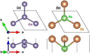
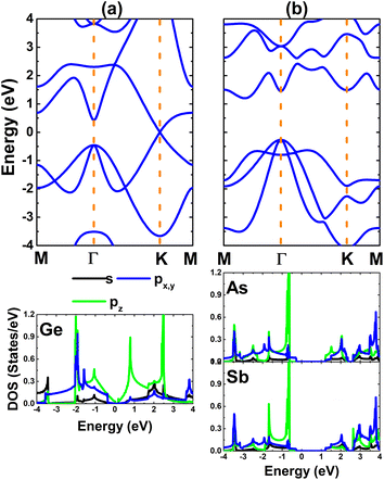
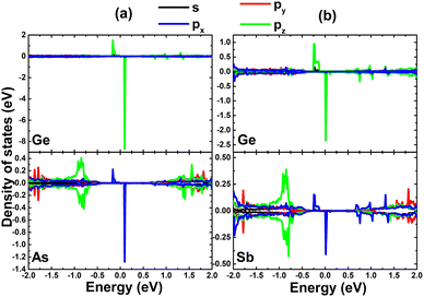
Germanene monolayers adopt a buckled hexagonal honeycomb structure, belonging to the P![[3 with combining macron]](https://www.rsc.org/images/entities/char_0033_0304.gif) m1 (no. 164) space group. There are two equivalent germanium (Ge) atoms in a unit cell as displayed in Fig. 1a. The structure of germanene is optimized by relaxing freely atomic positions and unit cell geometry. Our calculations yield the following optimal parameters: (1) lattice constant a = 4.06 Å; (2) chemical bond length dGe–Ge = 2.44 Å; (3) buckling height ΔGe–Ge = 0.69; and (4) interatomic angle ∠ = 112.34°, which are in good agreement with previous calculations.66 Fig. 2a shows the calculated electronic band structure and projected density of states (PDOS) of the germanene monolayer. The semimetallic character can be noted with a Dirac cone at the K point. In the considered energy from −4 to 4 eV, the band structure is formed from both the s orbital (s state) and p orbital (px,y and pz states). As a characteristic of hexagonal 2D materials, px and py are degenerate,67,68 and are submerged in both the valence band and conduction band of the germanene monolayer. Meanwhile, the pz state is the main contributor at the vicinity of the Fermi level to the Dirac cone.
m1 (no. 164) space group. There are two equivalent germanium (Ge) atoms in a unit cell as displayed in Fig. 1a. The structure of germanene is optimized by relaxing freely atomic positions and unit cell geometry. Our calculations yield the following optimal parameters: (1) lattice constant a = 4.06 Å; (2) chemical bond length dGe–Ge = 2.44 Å; (3) buckling height ΔGe–Ge = 0.69; and (4) interatomic angle ∠ = 112.34°, which are in good agreement with previous calculations.66 Fig. 2a shows the calculated electronic band structure and projected density of states (PDOS) of the germanene monolayer. The semimetallic character can be noted with a Dirac cone at the K point. In the considered energy from −4 to 4 eV, the band structure is formed from both the s orbital (s state) and p orbital (px,y and pz states). As a characteristic of hexagonal 2D materials, px and py are degenerate,67,68 and are submerged in both the valence band and conduction band of the germanene monolayer. Meanwhile, the pz state is the main contributor at the vicinity of the Fermi level to the Dirac cone.
 |
| | Fig. 1 Atomic structure (unit cell is marked) of (a) germanene and (b) AsSb monolayer. | |
 |
| | Fig. 2 Electronic band structure and projected density of states of (a) germanene and (b) AsSb monolayer. | |
A similar structure is considered for the AsSb monolayer (β phase) by alternating the arsenic (As) and antimony (Sb) atoms in a unit cell (see Fig. 1b). The following structural parameters can describe the optimized unit cell: (1) lattice constant a = 3.86 Å; (2) chemical bond length dAs–Sb = 2.70 Å; (3) wrinkle ΔAs–Sb = 1.52 Å; and (4) interatomic angle ∠AsSbAs = ∠SbAsSb = 91.47°. To examine the stability of this monolayer, the phonon dispersion curves are calculated. The results are displayed in Fig. 3. Considering two atoms (N = 2) in a primitive cell, the phonon spectra are composed of 3N = 6 phonon modes (between them 3 acoustic modes and 3N − 3 = 3 optical modes). Most importantly, there is no imaginary phonon frequency to confirm that the AsSb monolayer is dynamically stable. The band structure and PDOS spectra are given in Fig. 2b. The AsSb monolayer is an indirect gap semiconductor considering the valence band maximum (VBM) and conduction band minimum (CBM) located at the Γ point and along the MΓ direction, respectively. The obtained indirect gap value is 1.47 eV, which agrees well with previous calculations.58 In addition, HSE06-based calculations provide a larger band gap of 2.05 eV (see Fig. S1 of the ESI†). In the considered energy range, both constituents form the band structure: due to their similar valence electronic configurations, the As(4s24p3) and Sb(5s25p3) atoms exhibit similar PDOS spectra, where the band gap originates from the separation of electronic states belonging to the p orbitals.
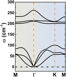 |
| | Fig. 3 Phonon dispersion curves of the AsSb monolayer. | |
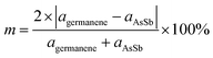
Next, the formation of lateral heterostructures was studied. The lattice mismatch m is calculated as follows:10
| |
 | (1) |
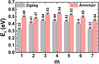
A small lattice mismatch of 5.05% is obtained, suggesting the feasibility of constructing lateral heterostructures from germanene and AsSb monolayers. In this work, a new set of (Ge)m–(AsSb)8−m with both armchair (A-) and zigzag (Z-) interlines are investigated. Fig. 4 shows the atomic structure of A-(Ge)4–(AsSb)4 and Z-(Ge)4–(AsSb)4 LHSs with 32 atoms in a unit cell, where the initial building blocks are clearly indicated. The formation energy Ef is calculated using the following expression:69
| | |
Ef = ELHS − 2mEgermanene − 2(8 − m)EAsSb
| (2) |
where the total energies of the LHS, germanene, and AsSb monolayer are denoted by
ELHS,
Egermanene, and
EAsSb, respectively. The results are given in
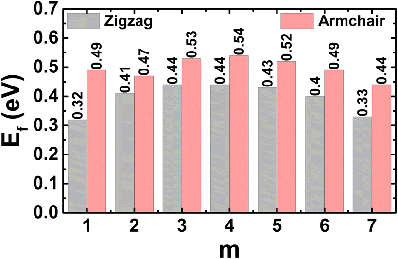
Fig. 5. A slight variation of
Ef with chemical composition is found. Moreover, the formation of A-LHSs (with
Ef between 0.44 and 0.54 eV) require higher energy than Z-LHSs (between 0.32 and 0.44 eV). In order to analyze the thermal stability of (Ge)
m–(AsSb)
8−m LHSs,
Ab Initio Molecular Dynamics (AIMD) simulations are carried out. The results indicate that all studied LHSs are thermally stable at 300 K considering the absence of structural destruction over a large time range of up to 3000 fs (see Fig. S2 of the ESI
†). It is suggested to prepare these LHSs by means of chemical vapor deposition
70 or molecular beam epitaxy,
71 methods which have been widely used to grow a large variety of 2D materials of large size and high quality. So far, experimental investigations have reported the preferable formation of a zigzag interface, meanwhile the armchair interline is only occasionally seen.
29,72 Therefore, germanene–AsSb Z-LHSs are expected to be formed more easily than their A-counterpart, which is in agreement with the calculated formation energies.
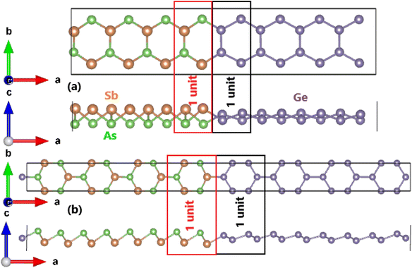 |
| | Fig. 4 Atomic structure of (a) armchair- and (b) zigzag-interline (Ge)4–(AsSb)4 lateral heterostructures. | |
 |
| | Fig. 5 Formation energy of (Ge)m–(AsSb)8−m lateral heterostructures with armchair- and zigzag-interline. | |
B. Armchair-interline lateral heterostructures
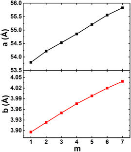
As a first step, the LHSs structures are optimized by freely relaxing the constituent atoms and unit cell geometry. Fig. 6 shows the calculated lattice constants. Remembering that germanene has a larger lattice constant than the AsSb monolayer, consequently, the LHSs unit cell dimensions increase nearly linearly with the number of germanene units. Moreover, there is an abrupt variation of the buckling height at the interface due to each side preserving its original wrinkle (see Fig. 4a).
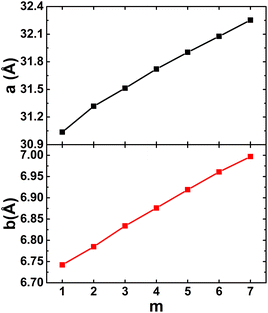 |
| | Fig. 6 Lattice constants of armchair-interline (Ge)m–(AsSb)8−m lateral heterostructures. | |
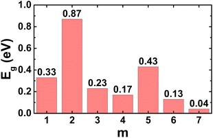
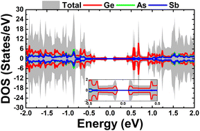
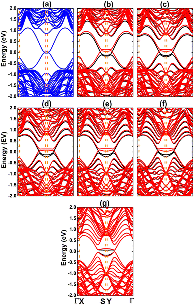
The calculated band structures are displayed in Fig. 7, which show the semiconductor nature of the armchair-interline lateral heterostructures. The direct gap character of (Ge)5–(AsSb)3 and (Ge)7–(AsSb)1 LHSs can be noted, considering the location of both the VBM and CBM at the X point, meanwhile the remaining LHSs are indirect gap semiconductors since their VBM and CBM take place at different high symmetry points. Therefore, the indirect-to-direct gap transition may occur by simply varying the number of building blocks in the lateral heterostructure. The calculated energy gaps are given in Fig. 8. Note that this parameter depends strongly on the chemical composition. The largest band gap of 0.87 eV is obtained with 25% germanene (m = 2). Meanwhile, a large germanene composition of 87.5% (m = 7) leads to a strong reduction of the band gap to 0.04 eV. From the atom-decomposed DOS spectra in Fig. 9, one can see that the Ge atom only, is the origin of the flat energy branches at the vicinity of the Fermi level, which mainly regulates the semiconductor phase of the lateral heterostructures. To obtain more insight into the band gap origin, the PDOS spectra of interline Ge atoms are calculated, the results are given in Fig. 10. One can see that both the upper part of the valence band and the lower part of the conduction band are formed mainly by the pz state. Such that the band gap appears due to the separation of Ge-pz and its value may be impacted by the charge redistribution in this electronic state, which depends on the width of germanene layers. Therefore, it can be concluded that the germanene monolayer band gap can be significantly increased by in-plane interfacial engineering with semiconductor monolayers.
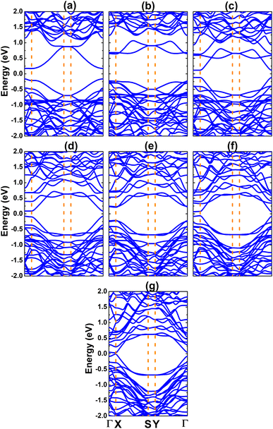 |
| | Fig. 7 Electronic band structure (blue curves: non-spin-polarization) of armchair-interline (Ge)m–(AsSb)8−m lateral heterostructures with (a) m = 1, (b) m = 2, (c) m = 3, (d) m = 4, (e) m = 5, (f) m = 6, and (g) m = 7. | |
 |
| | Fig. 8 Electronic band gap of armchair-interline (Ge)m–(AsSb)8−m lateral heterostructures. | |
 |
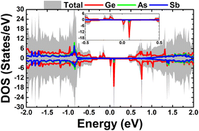
| | Fig. 9 Total and atom-decomposed density of states of the armchair-interline (Ge)4–(AsSb)4 lateral heterostructure. | |
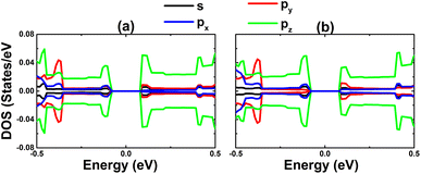 |
| | Fig. 10 Projected density of states of interline Ge atoms of armchair-interline (Ge)4–(AsSb)4 lateral heterostructure: Ge atom of (a) Ge–As and (b) Ge–Sb chemical bonds. | |
C. Zigzag-interline lateral heterostructures
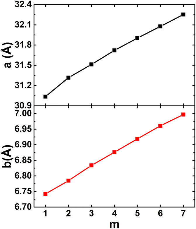
Similar to the previous cases of armchair-interline LHSs, the atomic structures of the zigzag structures are optimized before proceeding with the calculation of electronic and magnetic properties. The variation of unit cell dimensions as a function of chemical composition (number of germanene units) is illustrated in Fig. 11. As expected, the lattice constants increase in order to incorporate more germanene blocks into the lateral heterostructures to satisfy the size criterion, exhibiting a nearly linear relation.
 |
| | Fig. 11 Lattice constants of zigzag-interline (Ge)m–(AsSb)8−m lateral heterostructures. | |
Fig. 12 shows the calculated band structures of Z-(Ge)m–(AsSb)8−m LHSs considering the energy range −2 to 2 eV, where all exhibit clear spin polarization except for m = 1 (Fig. 12a). In all cases, the multivalley in both the valence band and conduction band, induces the quantum valley Hall effect. The valence band and conduction band are connected by flat energy branches, leading to the appearance of topological phases. Normally, the topological phases are obtained in nanoribbons, where the edge states connect the valence band and conduction band.73,74 Therefore, our results may introduce a new efficient approach to obtain a topological phase in 2D materials, with both gap and gapless topological interface states. Moreover, new (Ge)m–(AsSb)8−m LHSs can be considered as potential materials for spintronic applications with quantum spin-valley Hall effects. To analyze the band structure formation, the atom-decomposed DOS spectra are given in Fig. 13. Note that the flat states around the Fermi level are formed mainly from Ge atoms. Therefore, one can conclude that the interface states originate mainly from Ge atoms at the interfaces. Interestingly, the interface states show Weyl semimetal character with the presence of Fermi-arc states75 (see Fig. S3 of the ESI† for band structures from −0.5 to 0.5 eV) enriching the ground state properties of the studied lateral heterostructures, making them promising candidates for practical applications.
 |
| | Fig. 12 Electronic band structure (blue curve: non-spin-polarization; black curve: spin-up; red curve: spin-down) of zigzag-interline (Ge)m–(AsSb)8−m lateral heterostructures with (a) m = 1, (b) m = 2, (c) m = 3, (d) m = 4, (e) m = 5, (f) m = 6, and (g) m = 7. | |
 |
| | Fig. 13 Total and atom-decomposed density of states of zigzag-interline (Ge)4–(AsSb)4 lateral heterostructure. | |
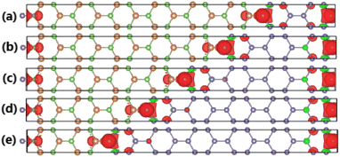
Interestingly, our simulations show the emergence of magnetism in zigzag-interline (Ge)m–(AsSb)8−m LHSs depending on their chemical composition. This feature is reflected in the total magnetic moments, which are given in Fig. 14. Note that the non-magnetic nature of separated monolayers is preserved when forming the (Ge)1–(AsSb)7 LHS. The magnetization takes place with germanene composition between 25% (m = 2) and 75% (m = 6) with magnetic moments between 0.46 μB and 0.49 μB. Meanwhile, a small value of only 0.01 μB is obtained for the (Ge)7–(AsSb)1 LHS, suggesting its low magnetization. The origin of magnetism is examined through the spin density illustrated in Fig. 15. From the figure, one can see that the magnetic properties are produced mainly at interfaces. Herein, the spin-up state of Ge atoms plays a key role in the origin of magnetism, meanwhile As and Sb atoms exhibit a small contribution. All these features agree well with the band structure profiles, where the spin polarization (m = 2 to 7) is observed only for edge states. The PDOS spectra of Ge, As, and Sb atoms at the interlines of (Ge)4–(AsSb)4 LHS are displayed in Fig. 16, as an example, to provide more insight. The degree of spin asymmetry can be attributed to the LHS magnetization of the Ge-pz state. However, we should not neglect the role of the Ge-s, As(Sb)-px, and As(Sb)-pz states considering their presence at the vicinity of the Fermi level, which generate the edge states along with the Ge-pz state.
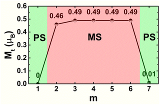 |
| | Fig. 14 Total magnetic moment Mt of zigzag-interline (Ge)m–(AsSb)8−m lateral heterostructures (PS: paramagnetic state; MS: magnetic state). | |
 |
| | Fig. 15 Spin density (red surface: spin-up state; green surface: spin-down state; iso-surface value: 0.0005 e Å−3) in (Ge)m–(AsSb)8−m lateral heterostructures with (a) m = 2, (b) m = 3, (c) m = 4, (d) m = 5, and (e) m = 6. | |
 |
| | Fig. 16 Projected density of states of the interline atoms of the zigzag-interline (Ge)4–(AsSb)4 lateral heterostructure: (a) Ge–As and (b) Ge–Sb chemical bonds. | |
IV. Conclusions
In summary, first-principles calculations have been performed to investigate the structural, electronic, and magnetic properties of germanene and AsSb monolayers, as well as their lateral heterostructures. Germanene is a 2D semimetal with Dirac cone at the K point. Meanwhile, the AsSb monolayer is proven to be dynamically stable and exhibits semiconductor character with a band gap of 1.47 eV. A small lattice mismatch of 2.53% may favor the formation of lateral heterostructures, where Z-LHSs are energetically more favorable than A-LHSs due to their smaller formation energy. Following the size criterion, the unit cell dimensions increase according to increasing germanene composition. The main contribution of Ge atoms at the vicinity of the Fermi level suggest a band gap increase of the germanene monolayer caused by the in-plane interfacial contact with semiconductor AsSb monolayer along the armchair line. Meanwhile, the Z-LHSs band structure shows rich electronic features with topological phase, where the valence band and conduction band are connected by interface states. The multivalley profiles of both the valence band and conduction band may suggest the quantum spin-valley Hall effects for different magnetic applications. In these cases, magnetic properties are produced mainly by the spin-up of interface Ge atoms (Ge-pz state). Our findings may pave a new way to obtain new 2D materials with either semiconductor or topological phases, with the latter rare in 2D materials at equilibrium.
Computational resources
Calculations were performed at the DGCTIC-UNAM Supercomputing Center (projects LANCAD-UNAM-DGTIC-368).
Data availability
The data that support the findings of this study are available from the corresponding author upon request.
Conflicts of interest
The authors declare that they have no known competing financial interests or personal relationships that could have appeared to influence the work reported in this paper.
Acknowledgements
This research is funded by the Vietnam National Foundation for Science and Technology Development (NAFOSTED) under grant number 103.03-2018.358. Pham Quynh Trang would like to extend her gratitude to Thai Nguyen University of Education for their support.
References
- K. S. Novoselov, A. K. Geim, S. V. Morozov, D.-e. Jiang, Y. Zhang, S. V. Dubonos, I. V. Grigorieva and A. A. Firsov, Electric field effect in atomically thin carbon films, Science, 2004, 306(5696), 666–669 CrossRef CAS PubMed
 .
. - M. J. Allen, V. C. Tung and R. B. Kaner, Honeycomb carbon: a review of graphene, Chem. Rev., 2010, 110(1), 132–145 CrossRef CAS PubMed .
- X. J. Lee, B. Y. Z. Hiew, K. C. Lai, L. Y. Lee, S. Gan, S. Thangalazhy-Gopakumar and S. Rigby, Review on graphene and its derivatives: Synthesis methods and potential industrial implementation, J. Taiwan Inst. Chem. Eng., 2019, 98, 163–180 CrossRef CAS .
- M. Tahriri, M. Del Monico, A. Moghanian, M. T. Yaraki, R. Torres, A. Yadegari and L. Tayebi, Graphene and its derivatives: Opportunities and challenges in dentistry, Mater. Sci. Eng., C, 2019, 102, 171–185 CrossRef CAS PubMed .
- K. K. Kim, A. Hsu, X. Jia, S. M. Kim, Y. Shi, M. Hofmann, D. Nezich, J. F. Rodriguez-Nieva, M. Dresselhaus and T. Palacios, et al., Synthesis of monolayer hexagonal boron nitride on Cu foil using chemical vapor deposition, Nano Lett., 2012, 12(1), 161–166 CrossRef PubMed .
- Z. Lin, M. T. Thee, A. L. Elías, S. Feng, C. Zhou, K. Fujisawa, N. Perea-López, V. Carozo, H. Terrones and M. Terrones, Facile synthesis of MoS2 and MoxW1−xS2 triangular monolayers, APL Mater., 2014, 2(9), 092514 CrossRef .
- H. Zhang, M. Holbrook, F. Cheng, H. Nam, M. Liu, C.-R. Pan, D. West, S. Zhang, M.-Y. Chou and C.-K. Shih, Epitaxial growth of two-dimensional insulator monolayer honeycomb BeO, ACS Nano, 2021, 15(2), 2497–2505 CrossRef CAS PubMed .
- B. Luo, Y. Yao, E. Tian, H. Song, X. Wang, G. Li, K. Xi, B. Li, H. Song and L. Li, Graphene-like monolayer monoxides and monochlorides, Proc. Natl. Acad. Sci. U. S. A., 2019, 116(35), 17213–17218 CrossRef CAS PubMed .
- H. Şahin, S. Cahangirov, M. Topsakal, E. Bekaroglu, E. Akturk, R. T. Senger and S. Ciraci, Monolayer honeycomb structures of group-IV elements and III-V binary compounds: First-principles calculations, Phys. Rev. B: Condens. Matter Mater. Phys., 2009, 80(15), 155453 CrossRef .
- H. Zheng, X.-B. Li, N.-K. Chen, S.-Y. Xie, W. Q. Tian, Y. Chen, H. Xia, S. Zhang and H.-B. Sun, Monolayer II-VI semiconductors: A first-principles prediction, Phys. Rev. B: Condens. Matter Mater. Phys., 2015, 92(11), 115307 CrossRef .
- A. Gupta, T. Sakthivel and S. Seal, Recent development in 2D materials beyond graphene, Prog. Mater. Sci., 2015, 73, 44–126 CrossRef CAS .
- J. R. Schaibley, H. Yu, G. Clark, P. Rivera, J. S. Ross, K. L. Seyler, W. Yao and X. Xu, Valleytronics in 2D materials, Nat. Rev. Mater., 2016, 1(11), 1–15 Search PubMed .
- B. Luo, G. Liu and L. Wang, Recent advances in 2D materials for photocatalysis, Nanoscale, 2016, 8(13), 6904–6920 RSC .
- J. An, X. Zhao, Y. Zhang, M. Liu, J. Yuan, X. Sun, Z. Zhang, B. Wang, S. Li and D. Li, Perspectives of 2D materials for optoelectronic integration, Adv. Funct. Mater., 2022, 32(14), 2110119 CrossRef CAS .
- H. Shu, X. Niu, X. Ding and Y. Wang, Effects of strain and surface modification on stability, electronic and optical properties of GaN monolayer, Appl. Surf. Sci., 2019, 479, 475–481 CrossRef CAS .
- T. Kuila, S. Bose, A. K. Mishra, P. Khanra, N. H. Kim and J. H. Lee, Chemical functionalization of graphene and its applications, Prog. Mater. Sci., 2012, 57(7), 1061–1105 CrossRef CAS .
- S. Tiwari, M. L. Van de Put, B. Sorée and W. G. Vandenberghe, Magnetic order and critical temperature of substitutionally doped transition metal dichalcogenide monolayers, npj 2D Mater. Appl., 2021, 5(1), 54 CrossRef CAS .
- D. Hoat, D. K. Nguyen, J. Guerrero-Sanchez, R. Ponce-Pérez, V. Van On, J. Rivas-Silva and G. H. Cocoletzi, Engineering the electronic and magnetic properties of nitrogene monolayer and bilayer by doping: A first-principles study, Appl. Surf. Sci., 2021, 566, 150711 CrossRef CAS .
- G. Zhang and Y.-W. Zhang, Strain effects on thermoelectric properties of two-dimensional materials, Mech. Mater., 2015, 91, 382–398 CrossRef .
- G. G. Naumis, S. Barraza-Lopez, M. Oliva-Leyva and H. Terrones, Electronic and optical properties of strained graphene and other strained 2D materials: a review, Rep. Prog. Phys., 2017, 80(9), 096501 CrossRef PubMed .
- D. Hoat, M. Naseri, R. Ponce-Pérez, N. N. Hieu, T. V. Vu, J. Rivas-Silva and G. H. Cocoletzi, Reducing the electronic band gap of BN monolayer by coexistence of P(As)-doping and external electric field, Superlattices Microstruct., 2020, 137, 106357 CrossRef CAS .
- K. K. Kim, H. S. Lee and Y. H. Lee, Synthesis of hexagonal boron nitride heterostructures for 2D van der Waals electronics, Chem. Soc. Rev., 2018, 47(16), 6342–6369 RSC .
- A. Azizi, S. Eichfeld, G. Geschwind, K. Zhang, B. Jiang, D. Mukherjee, L. Hossain, A. F. Piasecki, B. Kabius and J. A. Robinson, et al., Freestanding van der waals heterostructures of graphene and transition metal dichalcogenides, ACS Nano, 2015, 9(5), 4882–4890 CrossRef CAS PubMed .
- F. Li, B. Xu, W. Yang, Z. Qi, C. Ma, Y. Wang, X. Zhang, Z. Luo, D. Liang and D. Li, et al., High-performance optoelectronic devices based on van der Waals vertical MoS2/MoSe2 heterostructures, Nano Res., 2020, 13, 1053–1059 CrossRef CAS .
- F. Ceballos, M. Z. Bellus, H.-Y. Chiu and H. Zhao, Ultrafast charge separation and indirect exciton formation in a MoS2–MoSe2 van der Waals heterostructure, ACS Nano, 2014, 8(12), 12717–12724 CrossRef CAS PubMed .
- W. Liao, Y. Huang, H. Wang and H. Zhang, Van der Waals heterostructures for optoelectronics: progress and prospects, Appl. Mater. Today, 2019, 16, 435–455 CrossRef .
- Y. Liu, N. O. Weiss, X. Duan, H.-C. Cheng, Y. Huang and X. Duan, Van der Waals heterostructures and devices, Nat. Rev. Mater., 2016, 1(9), 1–17 Search PubMed .
- X.-Q. Zhang, C.-H. Lin, Y.-W. Tseng, K.-H. Huang and Y.-H. Lee, Synthesis of lateral heterostructures of semiconducting atomic layers, Nano Lett., 2015, 15(1), 410–415 CrossRef CAS PubMed .
- J. Zhao, K. Cheng, N. Han and J. Zhang, Growth control, interface behavior, band alignment, and potential device applications of 2D lateral heterostructures, Wiley Interdiscip. Rev.: Comput. Mol. Sci., 2018, 8(2), e1353 Search PubMed .
- J. Lee, S. Pak, Y.-W. Lee, Y. Park, A.-R. Jang, J. Hong, Y. Cho, B. Hou, S. Lee and H. Y. Jeong, et al., Direct epitaxial synthesis of selective two-dimensional lateral heterostructures, ACS Nano, 2019, 13(11), 13047–13055 CrossRef CAS PubMed .
- M. P. Levendorf, C.-J. Kim, L. Brown, P. Y. Huang, R. W. Havener, D. A. Muller and J. Park, Graphene and boron nitride lateral heterostructures for atomically thin circuitry, Nature, 2012, 488(7413), 627–632 CrossRef CAS PubMed .
- J. Wang, Z. Li, H. Chen, G. Deng and X. Niu, Recent advances in 2D lateral heterostructures, Nano-Micro Lett., 2019, 11, 1–31 CrossRef PubMed .
- M. E. Dávila and G. Le Lay, Few layer epitaxial germanene: a novel two-dimensional dirac material, Sci. Rep., 2016, 6(1), 1–9 CrossRef PubMed .
- Z. Qin, J. Pan, S. Lu, Y. Shao, Y. Wang, S. Du, H.-J. Gao and G. Cao, Direct evidence of Dirac signature in bilayer germanene islands on Cu (111), Adv. Mater., 2017, 29(13), 1606046 CrossRef PubMed .
- L. Kesper, J. A. Hochhaus, M. Schmitz, M. G. Schulte, U. Berges and C. Westphal, Tracing the structural evolution of quasi-freestanding germanene on Ag (111), Sci. Rep., 2022, 12(1), 7559 CrossRef CAS PubMed .
- L. Li, S.-z. Lu, J. Pan, Z. Qin, Y.-q. Wang, Y. Wang, G.-y. Cao, S. Du and H.-J. Gao, Buckled germanene formation on Pt (111), Adv. Mater., 2014, 26(28), 4820–4824 CrossRef CAS PubMed .
- M. Derivaz, D. Dentel, R. Stephan, M.-C. Hanf, A. Mehdaoui, P. Sonnet and C. Pirri, Continuous germanene layer on Al (111), Nano Lett., 2015, 15(4), 2510–2516 CrossRef CAS PubMed .
- L. Zhang, P. Bampoulis, A. Rudenko, Q. v. Yao, A. Van Houselt, B. Poelsema, M. Katsnelson and H. Zandvliet, Structural and electronic properties of germanene on MoS2, Phys. Rev. Lett., 2016, 116(25), 256804 CrossRef CAS PubMed .
- X.-S. Ye, Z.-G. Shao, H. Zhao, L. Yang and C.-L. Wang, Intrinsic carrier mobility of germanene is larger than graphene's: first-principle calculations, RSC Adv., 2014, 4(41), 21216–21220 RSC .
- M. Ezawa, Monolayer topological insulators: silicene, germanene, and stanene, J. Phys. Soc. Jpn., 2015, 84(12), 121003 CrossRef .
- M. Ye, R. Quhe, J. Zheng, Z. Ni, Y. Wang, Y. Yuan, G. Tse, J. Shi, Z. Gao and J. Lu, Tunable band gap in germanene by surface adsorption, Phys. E., 2014, 59, 60–65 CrossRef CAS .
- D. Hoat, D. K. Nguyen, R. Ponce-Perez, J. Guerrero-Sanchez, V. Van On, J. Rivas-Silva and G. H. Cocoletzi, Opening the germanene monolayer band gap using halogen atoms: An efficient approach studied by first-principles calculations, Appl. Surf. Sci., 2021, 551, 149318 CrossRef CAS .
- M. Köpf, N. Eckstein, D. Pfister, C. Grotz, I. Krüger, M. Greiwe, T. Hansen, H. Kohlmann and T. Nilges, Access and in situ growth of phosphorene-precursor black phosphorus, J. Cryst. Growth, 2014, 405, 6–10 CrossRef .
- W. Zhang, H. Enriquez, Y. Tong, A. Bendounan, A. Kara, A. P. Seitsonen, A. J. Mayne, G. Dujardin and H. Oughaddou, Epitaxial synthesis of blue phosphorene, Small, 2018, 14(51), 1804066 CrossRef PubMed .
- J.-S. Li, W.-L. Wang and D.-X. Yao, Band gap engineering of two-dimensional nitrogene, Sci. Rep., 2016, 6(1), 34177 CrossRef CAS PubMed .
- W. Lin, J. Li, W. Wang, S.-D. Liang and D.-X. Yao, Electronic structure and band gap engineering of two-dimensional octagon-nitrogene, Sci. Rep., 2018, 8(1), 1674 CrossRef PubMed .
- A. Carvalho, M. Wang, X. Zhu, A. S. Rodin, H. Su and A. H. Castro Neto, Phosphorene: from theory to applications, Nat. Rev. Mater., 2016, 1(11), 1–16 Search PubMed .
- A. H. Woomer, T. W. Farnsworth, J. Hu, R. A. Wells, C. L. Donley and S. C. Warren, Phosphorene: synthesis, scale-up, and quantitative optical spectroscopy, ACS Nano, 2015, 9(9), 8869–8884 CrossRef CAS PubMed .
- J. Shah, W. Wang, H. M. Sohail and R. Uhrberg, Experimental evidence of monolayer arsenene: an exotic 2D semiconducting material, 2D Mater., 2020, 7(2), 025013 CrossRef CAS .
- P. Jamdagni, A. Thakur, A. Kumar, P. Ahluwalia and R. Pandey, Two dimensional allotropes of arsenene with a wide range of high and anisotropic carrier mobility, Phys. Chem. Chem. Phys., 2018, 20(47), 29939–29950 RSC .
- Y. Shao, Z.-L. Liu, C. Cheng, X. Wu, H. Liu, C. Liu, J.-O. Wang, S.-Y. Zhu, Y.-Q. Wang and D.-X. Shi, et al., Epitaxial growth of flat antimonene monolayer: A new honeycomb analogue of graphene, Nano Lett., 2018, 18(3), 2133–2139 CrossRef CAS PubMed .
- D. Singh, S. K. Gupta, Y. Sonvane and I. Lukačević, Antimonene: a monolayer material for ultraviolet optical nanodevices, J. Mater. Chem. C, 2016, 4(26), 6386–6390 RSC .
- J. Zhou, J. Chen, M. Chen, J. Wang, X. Liu, B. Wei, Z. Wang, J. Li, L. Gu and Q. Zhang, et al., Few-layer bismuthene with anisotropic expansion for high-areal-capacity sodium-ion batteries, Adv. Mater., 2019, 31(12), 1807874 CrossRef PubMed .
- R.-B. Chen, D.-J. Jang, M.-C. Lin and M.-F. Lin, Optical properties of monolayer bismuthene in electric fields, Opt. Lett., 2018, 43(24), 6089–6092 CrossRef CAS PubMed .
- M. Long, A. Gao, P. Wang, H. Xia, C. Ott, C. Pan, Y. Fu, E. Liu, X. Chen and W. Lu, et al., Room temperature high-detectivity mid-infrared photodetectors based on black arsenic phosphorus, Sci. Adv., 2017, 3(6), e1700589 CrossRef PubMed .
- W. Yu, C.-Y. Niu, Z. Zhu, X. Cai, L. Zhang, S. Bai, R. Zhao and Y. Jia, Strain induced quantum spin hall insulator in monolayer β-BiSb from first-principles study, RSC Adv., 2017, 7(44), 27816–27822 RSC .
- X.-Y. Lin, F.-S. Meng, Q.-C. Liu, Q. Xue and H. Zhang, Semiconducting two-dimensional group VA–VA haeckelite compounds with superior carrier mobility, Phys. Chem. Chem. Phys., 2020, 22(21), 12260–12266 RSC .
- W. Yu, C.-Y. Niu, Z. Zhu, X. Wang and W.-B. Zhang, Atomically thin binary V–V compound semiconductor: a first-principles study, J. Mater. Chem. C, 2016, 4(27), 6581–6587 RSC .
- W. Kohn and L. J. Sham, Self-consistent equations including exchange and correlation effects, Phys. Rev., 1965, 140(4A), A1133 CrossRef .
- G. Kresse and J. Furthmüller, Efficiency of ab-initio total energy calculations for metals and semiconductors using a plane-wave basis set, Comput. Mater. Sci., 1996, 6(1), 15–50 CrossRef CAS .
- G. Kresse and J. Furthmüller, Efficient iterative schemes for ab initio total-energy calculations using a plane-wave basis set, Phys. Rev. B: Condens. Matter, 1996, 54(16), 11169 CrossRef CAS PubMed .
- J. P. Perdew, K. Burke and M. Ernzerhof, Generalized gradient approximation made simple, Phys. Rev. Lett., 1996, 77(18), 3865 CrossRef CAS PubMed .
- J. Heyd, G. E. Scuseria and M. Ernzerhof, Hybrid functionals based on a screened Coulomb potential, J. Chem. Phys., 2003, 118(18), 8207–8215 CrossRef CAS .
- A. V. Krukau, O. A. Vydrov, A. F. Izmaylov and G. E. Scuseria, Influence of the exchange screening parameter on the performance of screened hybrid functionals, J. Chem. Phys., 2006, 125(22), 224106 CrossRef PubMed .
- H. J. Monkhorst and J. D. Pack, Special points for Brillouin-zone integrations, Phys. Rev. B: Solid State, 1976, 13(12), 5188 CrossRef .
- M. Sun, Q. Ren, S. Wang, Y. Zhang, Y. Du, J. Yu and W. Tang, Magnetism in transition-metal-doped germanene: a first-principles study, Comput. Mater. Sci., 2016, 118, 112–116 CrossRef CAS .
- L. Pardini, S. Löffler, G. Biddau, R. Hambach, U. Kaiser, C. Draxl and P. Schattschneider, Mapping atomic orbitals with the transmission electron microscope: Images of defective graphene predicted from first-principles theory, Phys. Rev. Lett., 2016, 117(3), 036801 CrossRef PubMed .
- F. Ersan, E. Aktürk and S. Ciraci, Stable single-layer structure of group-V elements, Phys. Rev. B, 2016, 94(24), 245417 CrossRef .
- G.-X. Chen, X.-G. Li, Y.-P. Wang, J. N. Fry and H.-P. Cheng, Two-dimensional lateral GaN/SiC heterostructures: First-principles studies of electronic and magnetic properties, Phys. Rev. B, 2017, 95(4), 045302 CrossRef .
- G. H. Han, J. A. Rodríguez-Manzo, C.-W. Lee, N. J. Kybert, M. B. Lerner, Z. J. Qi, E. N. Dattoli, A. M. Rappe, M. Drndic and A. C. Johnson, Continuous growth of hexagonal graphene and boron nitride in-plane heterostructures by atmospheric pressure chemical vapor deposition, ACS Nano, 2013, 7(11), 10129–10138 CrossRef CAS PubMed .
- T. Ogikubo, H. Shimazu, Y. Fujii, K. Ito, A. Ohta, M. Araidai, M. Kurosawa, G. Le Lay and J. Yuhara, Continuous growth of germanene and stanene lateral heterostructures, Adv. Mater. Interfaces, 2020, 7(10), 1902132 CrossRef CAS .
- B. Kundu, P. Mohanty, P. Kumar, B. Nayak, B. Mahato, P. Ranjan, S. K. Chakraborty, S. Sahoo and P. K. Sahoo, Synthesis of lateral heterostructure of 2D materials for optoelectronic devices: challenges and opportunities, Emergent Mater., 2021, 4(4), 923–949 CrossRef CAS .
- B. Fu, M. Abid and C.-C. Liu, Systematic study on stanene bulk states and the edge states of its zigzag nanoribbon, New J. Phys., 2017, 19(10), 103040 CrossRef .
- K. W. Lee and C. E. Lee, Quantum valley Hall effect in wide-gap semiconductor SiC monolayer, Sci. Rep., 2020, 10(1), 5044 CrossRef CAS PubMed .
- X. Wan, A. M. Turner, A. Vishwanath and S. Y. Savrasov, Topological semimetal and Fermi-arc surface states in the electronic structure of pyrochlore iridates, Phys. Rev. B: Condens. Matter Mater. Phys., 2011, 83(20), 205101 CrossRef .
|
| This journal is © The Royal Society of Chemistry 2023 |
Click here to see how this site uses Cookies. View our privacy policy here. 
 Open Access Article
 This Open Access Article is licensed under a Creative Commons Attribution-Non Commercial 3.0 Unported Licence