
 Open Access Article
 This Open Access Article is licensed under a Creative Commons Attribution-Non Commercial 3.0 Unported Licence
Tunable ultra-broadband terahertz metamaterial absorber based on vanadium dioxide strips
Lilit Gevorgyan,
Hovhannes Haroyan *,
Henrik Parsamyan and
Khachatur Nerkararyan
*,
Henrik Parsamyan and
Khachatur Nerkararyan
Department of Microwave Physics, Yerevan State University, A. Manoogian 1, Yerevan, 0025, Armenia. E-mail: hharoyan@ysu.am
First published on 17th April 2023
Abstract
A simple design of an ultra-broadband metamaterial absorber (MMA) of terahertz (THz) radiation based on vanadium dioxide (VO2) configurations is proposed. The system is composed of a top pattern representing orderly distributed VO2 strips, a dielectric spacer and an Au reflector. Theoretical analysis based on the electric dipole approximation is performed to characterize the absorption and scattering properties of an individual VO2 strip. The results then are used to design an MMA composed of such configurations. It is shown that the efficient absorption characteristics of the Au–insulator–VO2 metamaterial structure can be ensured in a broad spectrum of 0.66–1.84 THz with an absorption band relative to the center frequency reaching as high as 94.4%. The spectrum of the efficient absorption can be easily tuned via the corresponding choice of strip dimensions. Wide polarization and incidence angle tolerance for both transverse electric (TE) and transverse magnetic (TM) polarizations are ensured by adding an identical parallel layer rotated by 90 degrees in respect to the first one. Interference theory is applied to elucidate the absorption mechanism of the structure. The possibility of modulation of the electromagnetic response of MMA relying on the tunable THz optical properties of VO2 is demonstrated.
Introduction
During the past two decades, the rapid development of high-frequency communication, medical, and sensing technologies attracted huge attention towards the terahertz spectrum of electromagnetic waves.1,2 Various metamaterial structures, representing periodic arrays of subwavelength unit cells, have been proposed to fill the technological gap of devices working in this spectrum. In particular, numerous metastructures for the amplitude and phase manipulation of the electromagnetic waves with applications in perfect absorption,3–5 sensing,6–8 focusing, filtering, polarization conversion,9–14 imaging,15 and modulation16,17 have been developed. Among these, perfect absorbers play a significant role in applications spanning from energy harvesting and detection to thermal emission.18,19 Depending on the spectral characteristics of the absorptance, single band, multiband and broadband MMAs are distinguished. To engineer an absorption band with various spectral properties, several common strategies are employed. For instance, single-band absorption can be easily ensured by simple unit-cell configurations, such as split-ring resonators, patches, and cut wires. Multi-band or broadband absorption characteristics can be engineered either by combining elements which are identical in shape but individually vary in size or different in shape.20–23 Moreover, the resonators can be arranged whether on the top surface of a unit cell (all in one plane) or stacked in a vertical direction. In ref. 23 the authors designed a polarization-insensitive MMA, where the relatively broad absorption band is due to merging the individual resonances of the double-open rectangular ring and strip cross-shape resonators both arranged on a unit-cell surface. On the contrary, in ref. 24 broadband absorption is engineered by utilizing a number of conductive bars of varying lengths stacked on three polyimide layers. Finally, the MMA presented in ref. 25 demonstrates broadband absorption by dividing the complete square ring structure into four sections and varying the characteristic size of each section. In general, the design of metamaterial absorbers includes metals as a reflector or resonator material. Although in the visible or infrared range, metals are characterized by high dispersion, at terahertz frequencies the conductivity of most metals is of the order of 106–107 S m−1, which does not provide wide control possibilities. In order to dynamically control the response of a metamaterial in the terahertz range, materials sensitive to an external stimulus (temperature, voltage, etc.) are used either as a spacer or resonator medium.26 For example, several semiconductors, such as Si and GaAs are characterized by pronounced photoactivity, making their material properties sensitive to external optical pumping.27,28 Graphene is another material whose conductivity can be effectively manipulated by an external voltage.26,29 Another way to achieve tunable electromagnetic response is by making use of a phase-changing material. VO2 is a common phase-changing material exhibiting an insulator-to-metal transition near ∼67 °C temperature resulting in a high conductivity of about 2 × 10⁵ S m−1. Consequently, by controlling the temperature, it is possible to change the conductivity of VO2 in a wide range, which gives wide control over metamaterials.30,31In this paper efficient broadband terahertz (THz) absorption of an elongated elliptical subwavelength configuration made of VO2 is investigated. The electric-dipole approximation is used to demonstrate the absorption enhancement of an elongated ellipsoid arising due to configurational resonance associated with a special combination of material properties and geometrical parameters. Finite element method-based simulations are conducted for a rectangular strip as an equivalent configuration for elongated oblate ellipsoid. It is shown that ordered arrangement of such strips on a surface of an Au-backed dielectric layer provides an absorption band exceeding 90% in a wide frequency range from 0.66 to 1.84 THz with the absorption bandwidth (BW) of ∼1.18 THz. The bandwidth relative to the center frequency of the absorption band (RBW) is ∼94.4%. Owing to controllable THz optical conductivity of VO2 the absorptance can be modulated from 0 up to 100% by varying the surrounding temperature. VO2 also provides an efficient platform for optimization and establishing prospective material characteristics for near-perfect absorption. Interference theory is applied to reveal the absorption mechanism.
Theory
Let a prolate ellipsoid with semi-axes az ≫ ay > ax, complex dielectric permittivity ε1 and embedded in a lossless dielectric medium ε2 be illuminated by a plane wave polarized along the largest semi-axis az. Considering the configuration in the quasi-static limits, i.e., when the largest semi-axis of a prolate ellipsoid satisfies the inequality condition kaz ≪ 1, where k is the wavenumber in the surrounding medium ε2, the dipole moment of a configuration is determined as:32| p = ε0ε2VχE, | (1) |
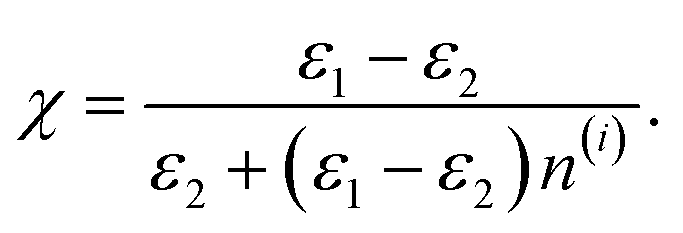 | (2) |
![[thin space (1/6-em)]](https://www.rsc.org/images/entities/char_2009.gif) ln(1.5/η) depends only the shape and sizes of a configuration, γ = ax/az and η = ay/az. The electric dipole polarizability of a configuration then has the following form:
ln(1.5/η) depends only the shape and sizes of a configuration, γ = ax/az and η = ay/az. The electric dipole polarizability of a configuration then has the following form:
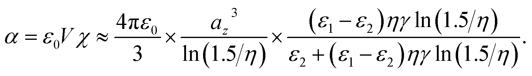 | (3) |
The absorption and scattering cross-sections of a particle can be defined as follows:32
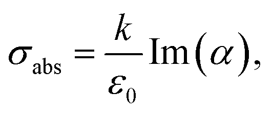 | (4) |
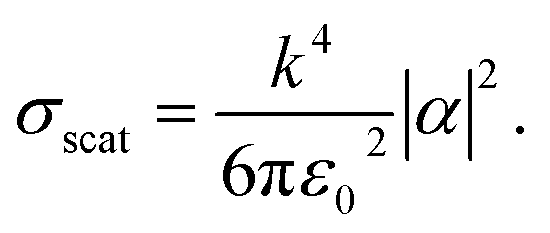 | (5) |
For quantitative analysis the absorption and scattering properties are normalized by the longitudinal geometrical cross-section area S = πayaz. The corresponding quantities called absorption and scattering efficiencies are:35
 | (6) |
Results and discussion
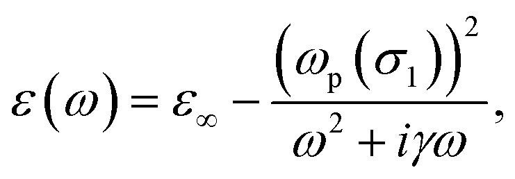
Analysis of the interaction of the elongated ellipsoidal subwavelength particles with plane electromagnetic waves shows that maximum absorption and minute scattering are achieved when the magnitude of the real part and the imaginary part of the dielectric permittivity of the spheroid medium are of the same order. Conductivities, and hence the imaginary part of the dielectric permittivities of common metals (such as Au, Ag, Cu, etc.) noticeably exceed the real part in magnitude as the frequency decreases. However, phase-changing materials can be exploited as their THz optical properties can be effectively manipulated by an external stimulus. Particularly, VO2 can undergo reversible phase transition from an insulator phase at the room-temperature to a ‘poor’ metallic phase at characteristic temperatures of ∼65–75 °C. The complex dielectric permittivity of VO2 in its metallic phase in the THz spectrum can be described according to Drude model,31
 | (7) |
 | (8) |
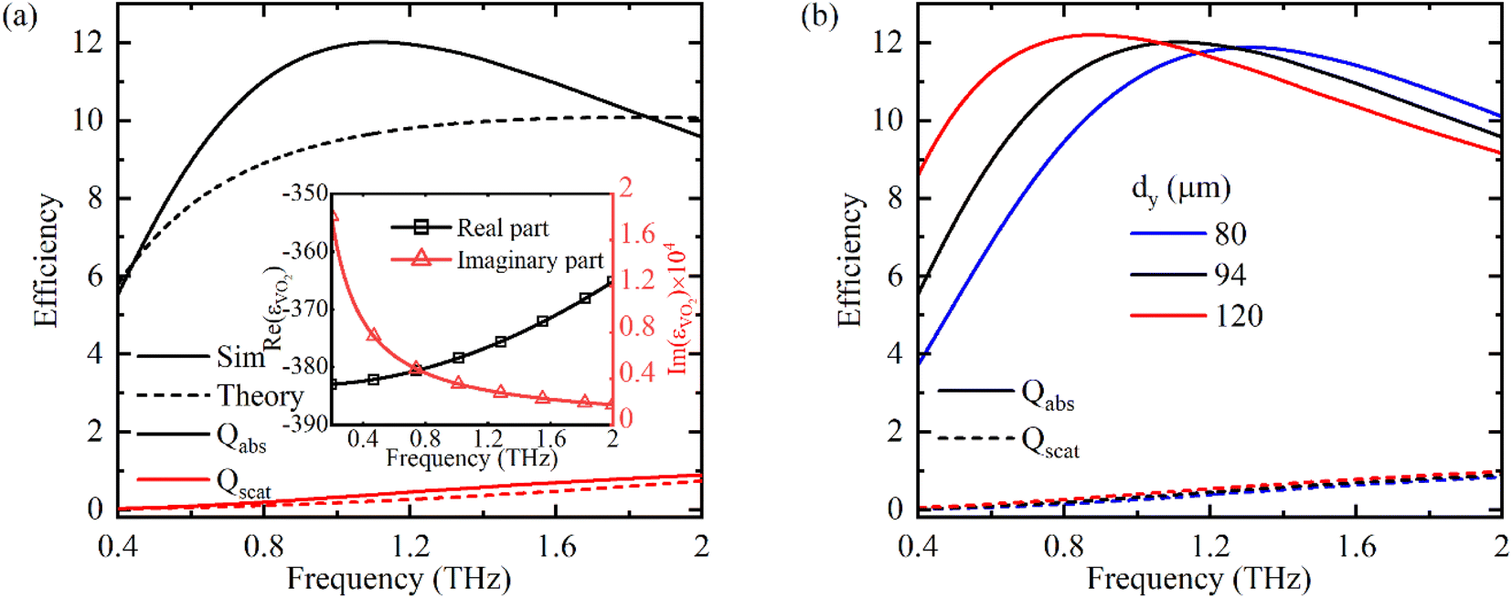 | ||
| Fig. 1 (a) Theoretical (dashed) and simulated (solid) absorption (black) and scattering (red) efficiency factors of ellipsoid- and strip-like VO2 configurations. The geometrical parameters for ellipsoid-strip are: ax = dx/2 = 0.5 μm, ay = dy/2 = 47 μm and az = dz/2 = 100 nm. (b) Absorption (solid lines) and scattering (dashed lines) efficiency spectra of strips with different height dy. Other geometrical sizes were kept constant. | ||
Analytical relation (3) derived within the quasistatic limits represents the depolarization factor of an oblate ellipsoid whose scattering and absorption efficiencies are shown in Fig. 1 by red and black solid lines, respectively. VO2 is used as a strip material and the surrounding medium is air.
Both the absorption and scattering efficiencies gradually increase as the frequency increases, however, the absorption is noticeably larger than the scattering and is around 10 at frequencies above 1 THz, whereas the Qscat is about 0.3. This means that the functional scattering surface of the configuration is much smaller than its geometrical cross-section. However, from a standpoint of integration with planar surfaces, a strip-like configuration can be promising also due to the fact that it is more straightforward for possible fabrication. Hence, hereinafter we use a strip-like configuration with identical geometrical parameters as those of an ellipsoid: the side lengths of the strip di in each coordinate direction are related to the semi-axes ai of the ellipsoid by the relation di = 2ai, where i = x, y, z.
Three-dimensional full-wave numerical simulations based on the finite element method were conducted to analyze the absorption and scattering properties of a VO2 strip. Absorption and scattering efficiencies of a strip are shown in Fig. 1 by black and red dashed lines, respectively. While the scattering properties of both configurations are similar, certain differences are observed between the absorption spectra. In particular, the absorption efficiency spectrum of a strip has resonant nature with a maximum value of about 12 at 1 THz. Here one should note that although the difference between the lateral cross-section areas of a strip and an ellipsoid is small, the volume of a strip is almost twice as large as that of the ellipsoid, which results in an increased absorption efficiency. Comparison of the simulated absorption and scattering properties of VO2 strips with dy values of 80, 94 and 120 μm are shown in Fig. 1(b). Solid lines stand for the absorption and dashed lines – for the scattering efficiency. As expected, a spectral shift towards lower frequencies is observed as dy increases. At the same time, the peak value of the absorption efficiency is almost constant and is around 12. Moreover, the scattering efficiency is negligibly small even when at the largest considered case of dy = 120 μm and barely reaches 0.4 at the peak frequency of 0.8 THz. In these calculations, dx and dz are as for Fig. 1(a). Once the conditions for the enhanced absorption dominating over the scattering are established for an individual strip-like configuration, we used the results above to design a VO2–dielectric–metal metamaterial for near-perfect broadband absorption of the THz irradiation. The metamaterial is composed of planar layers of an Au reflector and a dielectric spacer with nd = 1.5. We want to mention that the dielectric properties of a number of polymer materials, such as polypropylene36 and polyethylene cyclic olefin copolymer37 are suitable to use as a spacer. The third layer represents an array of VO2 strips periodically distributed on the top surface of a dielectric layer. A three-dimensional view of a metamaterial and the top view of the unit cell are depicted in Fig. 2(a). tm and td are the thicknesses of the bottom reflector and spacer, respectively, px and py are periodicities along the indicated directions, and dx and dy are the lateral dimensions of the strip. We used the optimized dimensions for strips and changed the periodicities and spacer thickness to achieve an efficient broad absorption band corresponding to the absorbance equal to or larger than 90%. Generally, the absorptance of the metamaterial is defined as A = 1 − R − T, where R and T are reflectance and transmittance. The latter are defined via frequency-dependent scattering parameters as R = |S11(f)|2 and T = |S21(f)|2. Since the transmission through the structure is blocked by a 3 μm-thick bottom Au layer (T = 0), which is much larger than its skin-depth (δs,Au ∼ 100 nm around 1 THz), the absorption coefficient is expressed only through the reflectance as A(f) = 1 − R(f). The absorption performance of the proposed system is investigated under the y-polarized plane wave. Fig. 2(b) plots the absorption spectrum for spacer thicknesses of 28 μm (green, diamonds) 32 μm (red, rings), 36 μm (black, squares) and 40 μm (blue, triangles). The sizes of a strip are chosen as in Fig. 1. As the spacer thickness decreases, the absorptance at lower frequencies drops below 0.9 level and a rising tendency of the absorptance at higher frequencies is observed. For instance, the efficient absorption band (A ≥ 0.9) for td = 28 μm is ∼1.11 THz (from 0.94 up to 2.05 THz), and that of td = 40 μm is ∼0.72 THz (from 0.59 up to 1.31 THz).
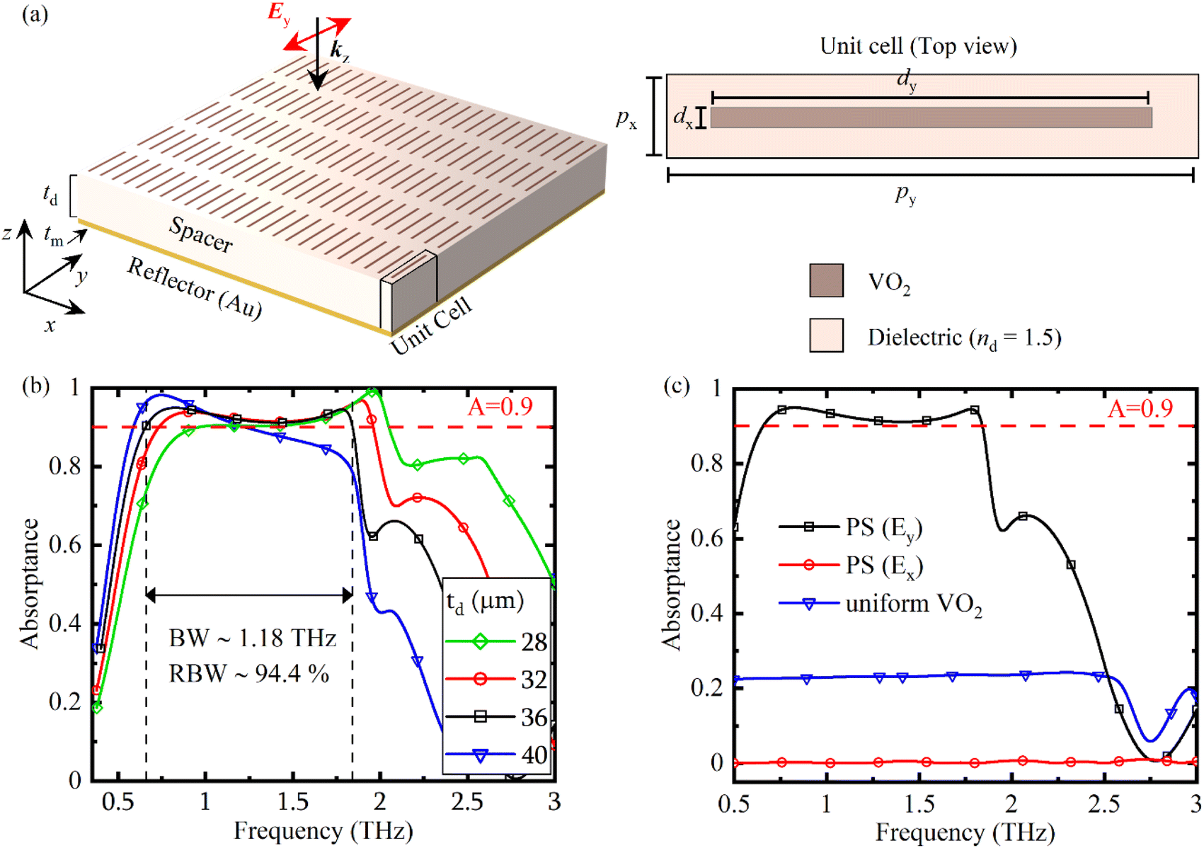 | ||
| Fig. 2 (a) 3D schematic of the periodic structure composed of an Au reflector, dielectric spacer with nd = 1.5 and rectangular VO2 strips as a unit-cell element; and the top-view of the unit cell, tm and td are the thickness of the reflector and spacer, respectively. (b) The absorption spectrum as a function of the thickness of the dielectric spacer. The geometrical parameters are as follows: td = 36 μm, tm = 3 μm, px = 6 μm, py = 114 μm, dz = 200 nm, dx = 1 μm and dy = 94 μm. (c) The absorption spectra of the periodic structure (PS) under x- and y-polarized plane waves (red and black lines, respectively), and the planar structure with strips replaced by a uniform VO2 layer (blue line). | ||
A compromise between the efficient absorption bandwidth and average absorptance above 0.9 is achieved for td = 36 μm. In this case, efficient absorption is achieved from 0.66 up to 1.84 THz with the absorption BW ∼ 1.18 THz. The average absorptance is about 0.93. Another criterion for the absorption performance is the relative bandwidth defined as RBW = BW/fc × 100%, which is about 94.4%. Although at td = 32 μm the absolute absorption BW (1.22 THz) is slightly larger than that of td = 36 μm (1.18 THz), our choice of the optimal spacer thickness of 36 μm is conditioned by the larger RBW and average absorptance of about 94.4% and 0.93, respectively, in contrast to 90% and 0.92 of the former case. Note that the total thickness of the optimized structure is 39.2 μm, which is around one-sixth of the centre wavelength of the efficient absorption band.
The structural asymmetry of the unit cell element dictates certain polarization dependence of the absorptance. Shown in Fig. 2(c) in red (circles) and black (squares) are the absorption spectra of the PS under x- and y-polarized plane waves. It is noted that near-perfect broadband absorption is achieved only when the incident field polarization is parallel to the longest side of strips, whereas, under cross-polarized radiation, strips do not interact with electromagnetic waves which are completely reflected from the bottom Au layer. To find out how the strip-like pattern of the top interface affects the absorption characteristics of the system, in Fig. 2(c) we compared the absorptance of the main design of the MMA with that of a planar Au–dielectric–VO2 structure (from bottom to top) shown by a blue-triangles line. The absorptance of the dielectric spacer sandwiched by 3 μm-thick Au and 200 nm-thick VO2 layers is around 0.22 at the entire considered spectrum up to 2.5 THz, whereas introducing rectangular strips noticeably enhances the absorptance ensuring near-perfect absorption characteristics. The absorption here is mainly conditioned by the attenuation of the electromagnetic waves while passing forward and backward through a thin and lossy VO2 top layer.
The next step includes optimization of the lateral sizes of the unit cell while keeping the strip sizes constant. The absorption spectra for different values of periodicities px and py are shown in Fig. 3(a) and (b), respectively. The absorption performance alters in a similar manner when either of the periodicities is increased, namely, the bandwidth is decreased and the overall absorptance is increased. The values of px = 6 μm and py = 114 μm were found to be optimal to ensure a broad efficient absorption band. Starting from py = 114 μm, a solid broad efficient absorption band is formed, and at larger values of py the average absorption constantly increases and the BW decreases. Such a behaviour can be attributed to reducing the coupling between neighbouring strips when their distance increases, which results in dominant configuration resonances of individual strips. Since all strips are identical, the resonance conditions also match. When the distance between strips is too large to establish coupling between neighbouring strips with a different frequency of the coupled system, resonant absorption bandwidth decreases.
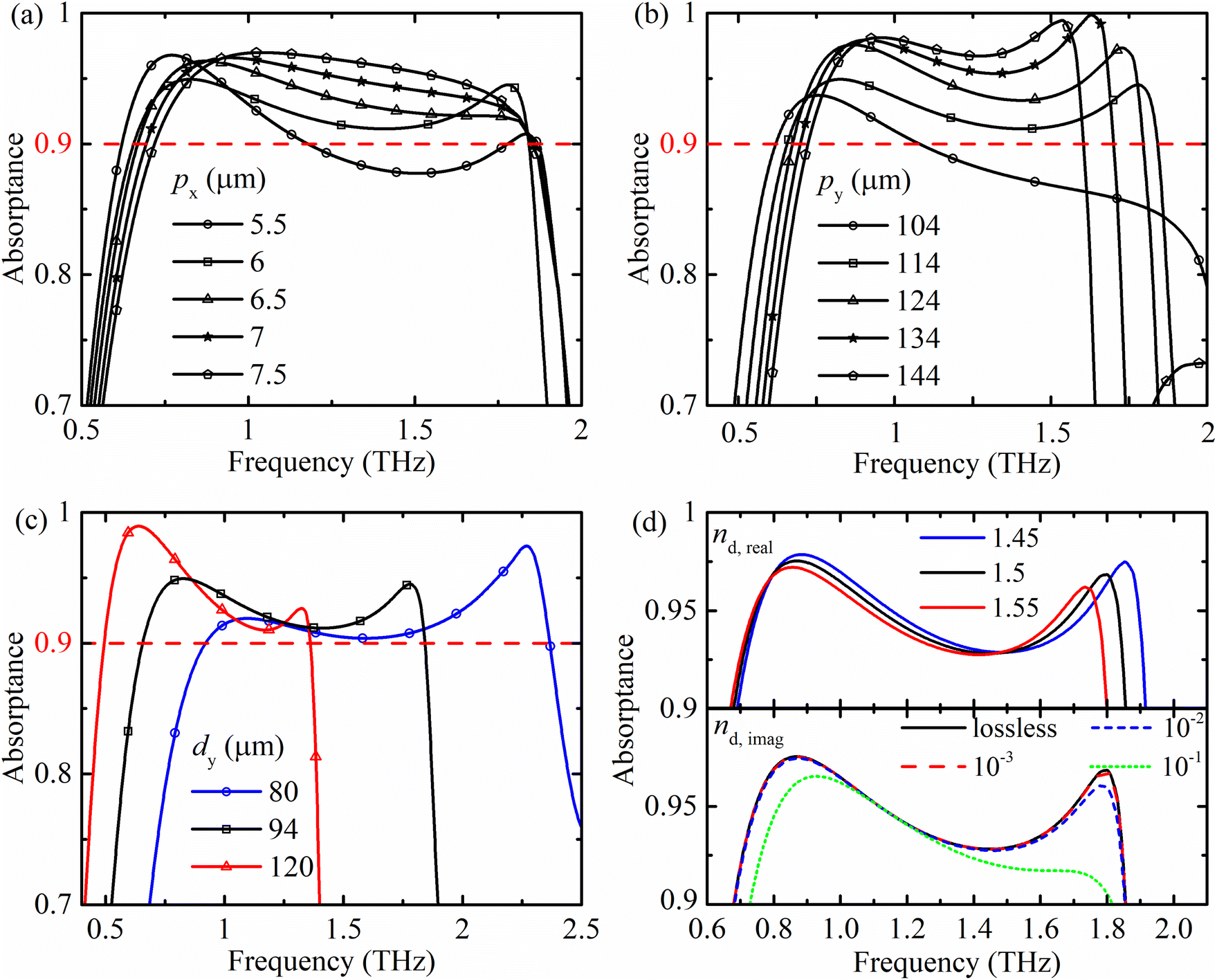 | ||
| Fig. 3 The absorption spectrum at different values of unit-cell periodicities (a) px (5.5, 6, 6.5, 7, 7.5 μm) and (b) py (104, 114, 124, 134 and 144 μm). (c) Absorption spectra of the optimized periodic structures with strips having different dy sizes. (d) The absorption spectra at different values of the real (top) and imaginary (bottom) parts of the spacer refractive index. The spacer is lossless in the top plot and the real part is 1.5 – in the bottom. The optimized sizes are: (i) dy = 120 μm, py = 140 μm, td = 44 μm, (ii) dy = 80 μm, py = 95 μm, td = 26 μm. Other parameters are as above. | ||
From the results presented in Fig. 1(b), one sees that the corresponding choice of the strip dimensions can alter the absorption spectrum. Fig. 3(c) sums up the tunability of the efficient absorptance spectrum of the MMA by varying the unit cell element sizes. First, a strip length is chosen with other geometrical parameters of the strip fixed and then the unit-cell dimensions were optimized to achieve a relatively broad absorption band. In particular, shown by red (triangles), black (squares) and blue (rings) lines (symbols) are the absorption spectra for the MMA with dy of 80, 94 and 120 μm, respectively. One notes that the efficient absorption spectrum gradually shifts to the higher frequencies as the strip length decreases, also resulting in the broadening of the absorption band. For instance, at dy = 120 μm the absorption band lays in 0.49–1.36 THz, with the corresponding BW (RBW) of 0.87 THz (94%). On the other hand, the efficient absorption band at dy = 80 μm expands from 0.92 up to 2.37 THz, with BW (RBW) of 1.45 THz (88%). These results clearly demonstrate the tunability of the suggested periodic structure, in all the considered cases achieving relative bandwidths around 90%. Finally, the top and bottom plots in Fig. 3(d) show the absorption spectra at different values of the real and imaginary parts of the spacer refractive index, respectively. Although the absorption BW slightly increases as the real part of the refractive index decreases, our choice of the real part of the substrate refractive index is 1.5 since it is characteristic of many commercially available polymers in the THz spectrum, such as polypropylene,36 high-density polyethylene,36 polyethylene cyclic olefin copolymer.37 On the other hand, the absorption spectrum is mainly independent of the spacer dielectric losses, hence supporting the practical implementation and widening the possible choice of spacer materials.
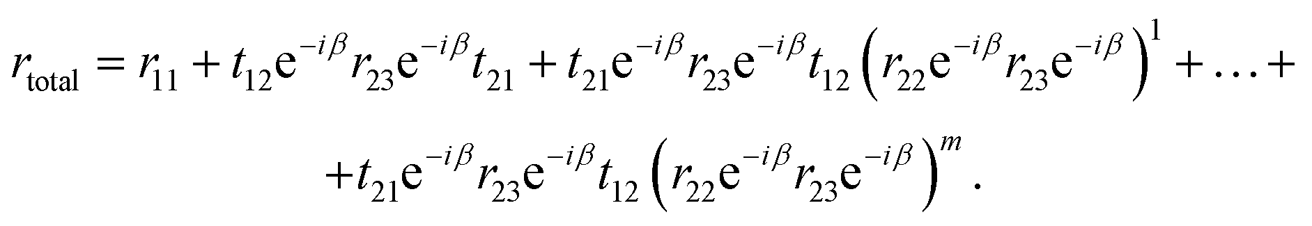
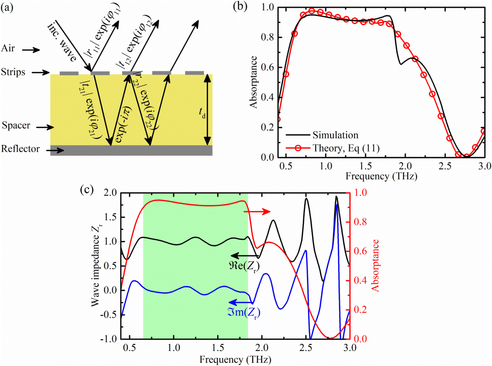
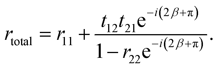
To examine the physical concept of the absorption mechanism and theoretically validate our results, we adopt interference theory based on the modified Fabry–Perot resonant model. In this theory, a metamaterial absorber is represented as a Fabry–Perot resonator, where the ground reflector serves as a perfect mirror and the top interface of strips is a partially reflective mirror.38 The schematic of the multiple reflections model within a metamaterial absorber is illustrated in Fig. 4(a). The plane electromagnetic wave impinging on the top interface of the metamaterial is partially reflected back to the air region and transmitted into the dielectric spacer with corresponding complex coefficients of r11 = |r11|exp(iφ11) and t21 = |t21|exp(iφ21). The latter waves are then totally reflected from the ground reflector and then divide into reflected and transmitted waves upon incidence on the top interface from the spacer side with the transmission coefficient of t12 = |t12|exp(iφ12) and reflection coefficient of r22 = |r22|exp(iφ22). Here φij represent the corresponding phase shift. The propagation phase is β = kh, where k is the wavenumber in the spacer and h is the path length of the beam inside the spacer. For a normal incidence h = td. According to the wave propagation theory in multilayer structures the total reflection coefficient of the layered system is determined as:38
 | (9) |
 | ||
| Fig. 4 (a) The schematic of the multiple reflections model within a metamaterial absorber. (b) Comparison of the absorptance of the proposed MMA derived via numerical simulations (black) and calculated by the interference theory, eqn (11) (red-rings). (c) The real and imaginary parts of the relative effective wave impedance of the absorber (left axis) and absorptance spectrum (right axis). The highlighted region corresponds to the efficient absorption spectrum. | ||
Assuming that the reflection coefficient from the ground plane r23 = −1 and applying some mathematical manipulations with the interaction number m ≫ 1, the total reflection coefficient can be simplified to
 | (10) |
The absorption hence is conditioned by the destructive interference between all r11 and t12 waves (multiple transmissions from spacer–strips interface to air). Since the transmittance from the ground metal layer T = 0, the total absorptance of the metamaterial is defined as
| A(ω) = 1 − R(ω) = 1 − |rtotal|2. | (11) |
The complex reflection/transmission coefficients used in the interference theory were calculated via the so-called decoupled model.38 The spectrum of the absorptance of the MMA calculated by eqn (7) of the interference theory and its comparison to that of obtained by simulation is shown in Fig. 4(b) by red-rings and solid black lines, respectively. One sees that the numerically and theoretically obtained results are in good agreement.
According to the impedance matching theory, a metamaterial structure perfectly absorbs the incident electromagnetic radiation when its complex effective wave impedance is matched to that of the wave impedance of the environment.31,38 Hence, when the total reflectance R(ω) of the structure approaches zero (A(ω) approaches 1), the wave impedance tends to match that of the free space. The relative impedance can be calculated by the following expression
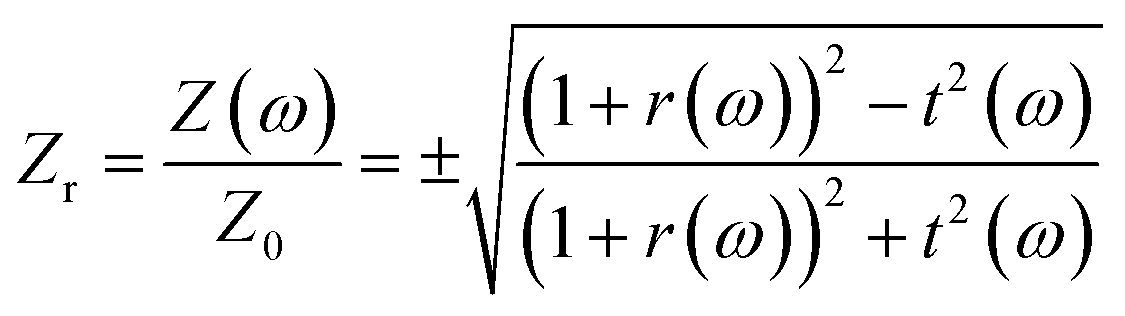 | (12) |
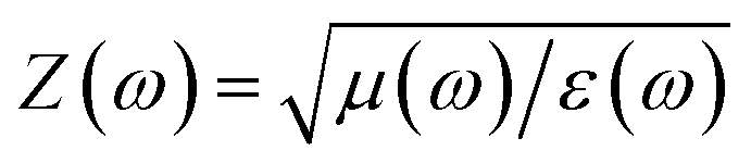 is the effective impedance of the metamaterial structure, μ and ε are the effective complex magnetic permeability and dielectric permittivity of the absorber, respectively, and Z0 ≈ 377 Ω is the wave impedance of air. In order to ensure efficient absorption in a given spectral range, the real part of the relative impedance
  need to approach 1, whereas the imaginary part
  needs to be equal to 0. Fig. 4(c) plots the real (black) and imaginary (blue) parts of the relative wave impedance Zr linked to the left axis, whereas the right axis shows the absorptance spectrum. The green highlighted region corresponds to the spectral region of the efficient absorption (A(ω) ≥ 0). It is seen that in the highlighted spectrum from 0.64 up to 1.81 THz
  whereas
  demonstrating the impedance matching of the absorber with the free space. Once the real and imaginary parts strongly deviate from those of the free space (below 0.64 THz and above 1.81 THz), the absorptance decreases noticeably. The main advantage of employing VO2 in THz technologies is that its conductivity can be controlled by temperature, allowing for a phase transition from dielectric to metallic states. Hence, the influence of the conductivity of the strip on the performance of MMA is also explored and the results are shown in Fig. 5(a). Here the conductivity σ of VO2 was changed from 200 S m−1 (insulating phase) to 2 × 10⁵ S m−1 (metallic phase). It is seen that in the insulating phase of strips, the absorptance of the periodic system is around 0 and MMA acts as a perfect mirror due to the bottom Au reflector. The absorptance gradually increases as the conductivity increases, with the absorptance spectrum having a Gaussian-like shape with a maximum at a constant frequency of 1.4 THz. When the VO2 strips are in a fully conductive state (σ = 2 × 10⁵ S m−1), a broad efficient absorption band is formed.
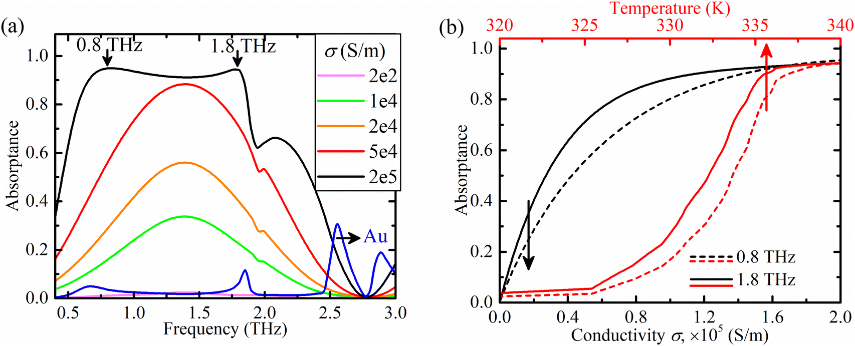 | ||
| Fig. 5 (a) The spectrum of the absorptance for different values of the VO2 conductivity and that for the Au strip. (b) Dependence of the absorptance on the conductivity σ of VO2 (black, bottom axis) and temperature (red, top axis) at 0.8 THz (dashed lines) and 1.8 THz (solid lines). | ||
Two maxima are observed in the efficient absorption band at 0.8 THz and 1.8 THz both having absorptance peak values of ∼0.94. Shown by a blue line in Fig. 5(a) is the absorption spectrum of a system with Au strips, where a 4.56 × 10⁷ S m−1 value for the THz conductivity was used.39 No broadband absorption is observed for highly conductive strip material but only several absorption peaks are present with the highest one at around 2.55 THz and a peak value of about 0.32. The dependence of the absorptance on the conductivity of VO2 (bottom axis, black) and temperature (top axis, red) are plotted in Fig. 5(b) at frequencies of 0.8 THz and 1.8 THz by dashed and solid lines, respectively. At both frequencies, the absorptance sharply increases by increasing the conductivity and starting from 1.14 × 10⁵ S m−1 at 0.8 THz and 1.42 × 10⁵ S m−1 at 1.8 THz the absorptance exceeds 90%. Since the conductivity of VO2 is proportional to the temperature, analogous dependence is also expected when the temperature is varied. Effective absorption is provided at temperatures above 336.9 and 335.6 K at frequencies of 0.8 and 1.8 THz, correspondingly. Thus, the absorptance can be effectively changed from 0.03 at (0.05) at 325 K to 0.95 (0.94) at 340 K when the frequency of the incident radiation is 0.8 THz (1.8 THz). This fact opens up the possibility to realize modulation of the amplitude of THz radiation. Moreover, the modulation depth can be tuned by controlling the temperature of the MMA structure.
In the above analysis, we chose an incident wave having a polarization parallel to the longest dimension of the strip to ensure efficient absorption. On the other hand, rotating the polarization by 90° in the lateral plane produces no absorption and all the electromagnetic waves are reflected. In other words, due to structural asymmetry, the absorption performance is sensitive to the incident field polarization. Polarization-insensitive absorption characteristics can be ensured by adding an additional parallel layer with strips oriented perpendicular to the first layer elements. The schematic of a super-cell of such an absorber and its absorption spectra under x- and y-polarized plane waves are shown in Fig. 6(a) and a two-dimensional map of the absorptance as a function of the frequency and polarization angle at normal incidence is shown in Fig. 6(b). Since the second layer of strips is closer to the Au reflector and is completely embedded in the dielectric spacer, a small difference is seen between absorption spectra of x- and y-polarized plane waves, as follows from Fig. 6(a). One sees that an efficient absorption band with a constant bandwidth is achieved for the entire range of polarization angles from 0° up to 90° [Fig. 6(b)]. The total optimized sizes of a supercell are td = 36 μm, px = 6 μm, py = 114 μm, dz = 200 nm, dx = 1 μm and dy = 94 μm, and the distance between two layers of strips is 3 μm. Finally, the performance of the polarization-insensitive design of the absorber under oblique incident TE and TM waves is shown in Fig. 7(a) and (b), respectively, with the corresponding illustrations of orientations of the electromagnetic field components.
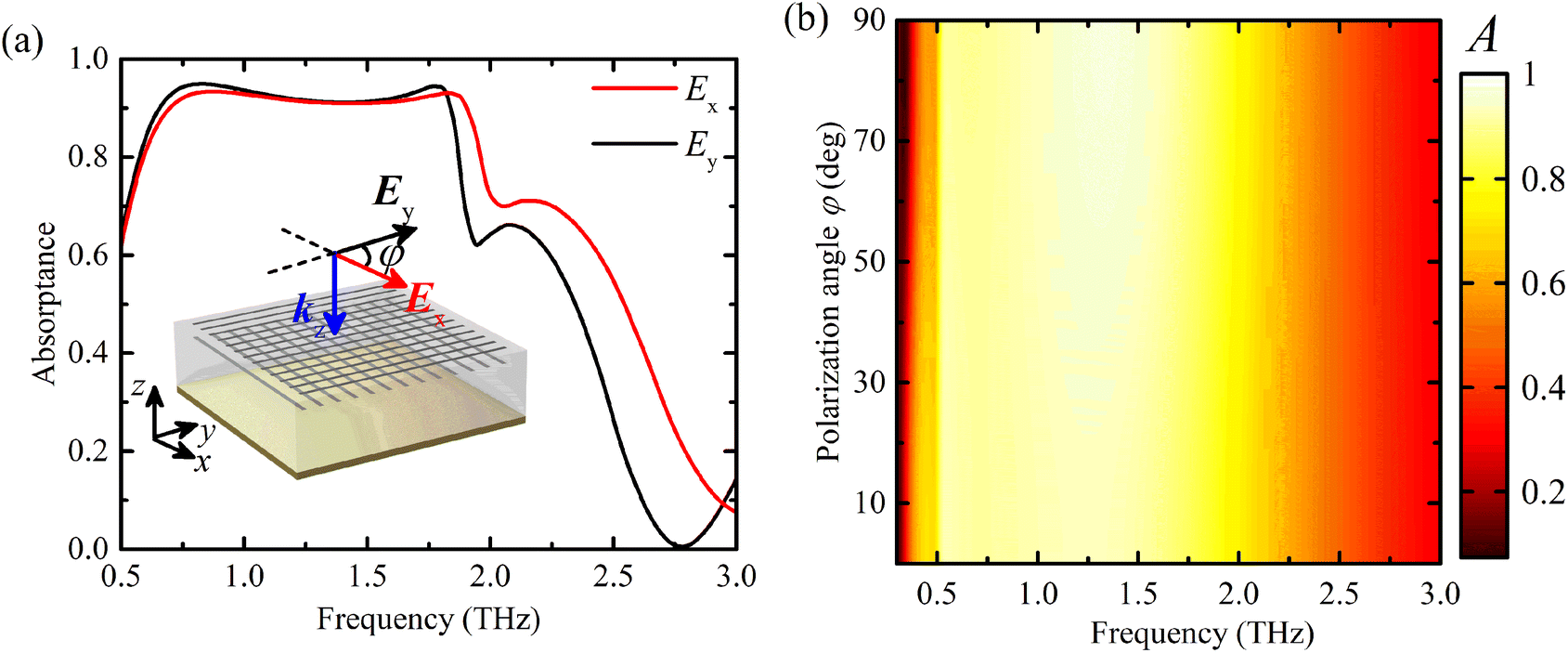 | ||
| Fig. 6 (a) The absorption spectrum of the system with two cross-oriented layers of strips under x- and y-polarized normally incident plane waves. The inset depicts the schematic of the super-cell. (b) The color map plot of absorptance spectrum as a function of the polarization angle φ. | ||
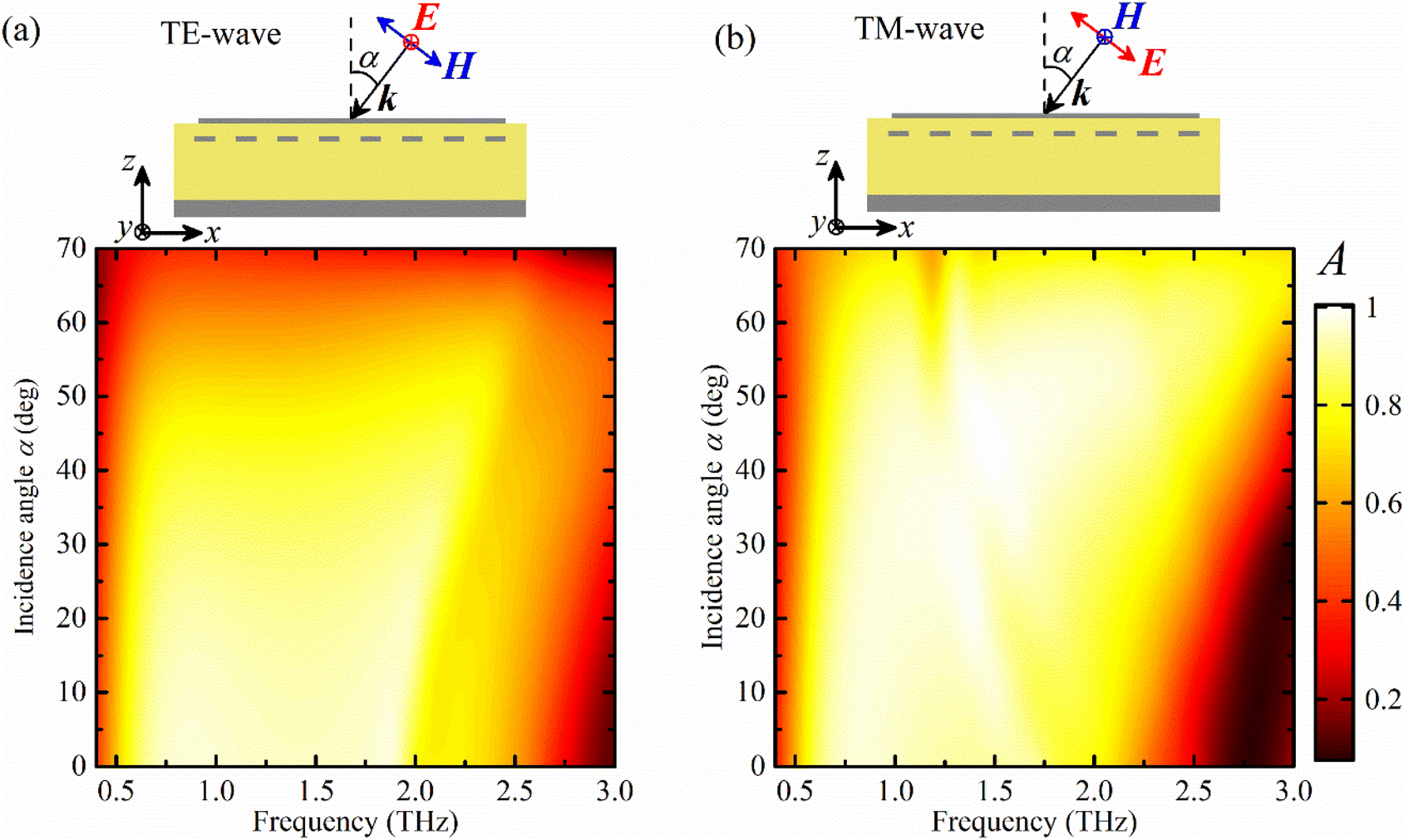 | ||
| Fig. 7 Absorptance spectrum of the structure as a function of the incidence angle α in the case of (a) TE-polarized waves and (b) TM-polarized waves with the corresponding schematic illustrations. | ||
Under the oblique incident TE-polarized waves the system preserves its broadband absorption performance for angles of incidence up to 40°, and the further increase in α gradually decreases the absorptance. Under TM polarized waves a continuous efficient absorption band is observed at incidence angles up to 55°.
Table 1 compares the performance of the proposed MMA with several structures reported in the literature which work in the same spectrum. The comparison criteria are 90% absorption band, BW, RBW, unit cell sizes, materials used and structural layers, as well as a short description on the unit-cell configurations used.
| Ref. | 90% absorption band (BW) in THz | RBW (%) | Unit cell sizes (μm3) | Materials (layers) | Structure |
|---|---|---|---|---|---|
| 40 | 0.39–0.72 (0.33) | 60 | 174 × 174 × 70.52 | Au, SiO2, VO2 (4) | Metallic cross resonators on SiO2–VO2–SiO2 planar structure |
| 41 | 0.457–1 (0.543) | 74.5 | 150 × 150 × 50.4 | Aluminium, polyimide (3) | Two symmetrical L-shaped metallic resonators |
| 20 | 1.58–2.22 (0.642) | 33.7 | 120 × 120 × 20.8 | Au, polyimide (5) | Two layers of four different sized square metallic patches |
| 22 | 0.61–1.36 (0.75) | 76.1 | 120 × 120 × 66 | SiO2, VO2, Au (3) | Ring and cross-like resonators with different sizes combined in a unit-cell and embedded in a dielectric layer |
| 42 | 1.33–2.43 (1.1) | 58.5 | 100 × 100 × 13.2 | Au, SiO2 (3) | Two double square split-ring resonators combined with three double circular split-ring resonators with different orientations |
| This paper | 0.66–1.84 (1.18) | 94.4 | 114 × 114 × 39.2 | VO2, polymer, Au (4) | Rectangular strips |
Conclusions
Thus, an ultra-broadband MMA of THz radiation based on VO2–insulator–metal configuration is proposed. The top pattern of MMA represents orderly distributed VO2 strips separated by a dielectric spacer from the bottom Au reflector. Theoretical analysis based on the electric dipole approximation is performed to characterize the absorption and scattering properties of individual elements. Finite element method-based simulations are carried out for a rectangular strip as an equivalent configuration for an elongated oblate ellipsoid. It is shown that the ordered distribution of such strips on a surface of an Au-backed planar dielectric provides absorptance exceeding 90% in a wide frequency range from 0.66 to 1.84 THz with a BW of about 1.18 THz. The corresponding relative bandwidth with respect to the centre frequency of the absorption band is ∼94.4%. Tunability of the absorption spectrum by varying dimensions of VO2 strips is demonstrated. The possibility of achieving wide polarization and incidence angle tolerance for both TE and TM polarizations is shown by making use of two parallel layers of VO2 strips rotated by 90 degrees with respect to each other. Controllable THz optical conductivity of VO2 opens up the prospects for modulation of the absorptance from 0 up to 100% by varying the surrounding temperature from 320 K to 340 K. Interference theory is applied to reveal the absorption mechanism and impedance-matching conditions for efficient absorption are clarified. We believe that our results can serve as a practical guideline for establishing suitable material and geometrical parameters of a simple MMA design capable of efficient broadband absorption in various parts of the EM spectrum.Author contributions
The authors have contributed to this article in the following way: Lilit Gevorgyan designed the tunable ultra-broadband terahertz metamaterial absorber based on vanadium dioxide strips using numerical simulation software and wrote the paper. Hovhannes Haroyan oversaw the entire process of organizing work, providing theoretical and simulation guidance and reviewing the manuscript. Henrik Parsamyan supervised the construction of the simulation model, proposed effective options for the design of the absorber, carried out the simulation and theory calculation, and wrote the article. Khachatur Nerkararyan conceived the presented idea, performed theoretical calculations, and analysed the results.Conflicts of interest
There are no conflicts of interest to declare.Acknowledgements
This work was supported by a scientific research grant through the Science Committee of MESCS of Armenia (21AG-1C061) and by a Faculty Research Funding Program 2022 implemented by Enterprise Incubator Foundation with the support of PMI Science. We also sincerely thank the RSC Advances staff for carefully preparing our manuscript's proofs.Notes and references
- C. Chen, M. Chai, M. Jin and T. He, Terahertz Metamaterial Absorbers, Adv. Mater. Technol., 2022, 7, 2101171 CrossRef CAS.
- W. Xu, L. Xie and Y. Ying, Mechanisms and applications of terahertz metamaterial sensing: a review, Nanoscale, 2017, 9, 13864–13878 RSC.
- Z. Zheng, Y. Luo, H. Yang, Z. Yi, J. Zhang, Q. Song, W. Yang, C. Liu, X. Wu and P. Wu, Thermal tuning of terahertz metamaterial absorber properties based on VO2, Phys. Chem. Chem. Phys., 2022, 24, 8846–8853 RSC.
- Y. Zhang, P. Wu, Z. Zhou, X. Chen, Z. Yi, J. Zhu, T. Zhang and H. Jile, Study on Temperature Adjustable Terahertz Metamaterial Absorber Based on Vanadium Dioxide, IEEE Access, 2020, 8, 85154–85161 Search PubMed.
- B.-X. Wang, Y. He, P. Lou and W. Xing, Design of a dual-band terahertz metamaterial absorber using two identical square patches for sensing application, Nanoscale Adv., 2020, 2, 763–769 RSC.
- B. M. A. Rahman, C. Viphavakit, R. Chitaree, S. Ghosh, A. K. Pathak, S. Verma and N. Sakda, Optical Fiber, Nanomaterial, and THz-Metasurface-Mediated Nano-Biosensors: A Review, Biosensors, 2022, 12, 42 CrossRef CAS PubMed.
- B.-X. Wang, W.-Q. Huang and L.-L. Wang, Ultra-narrow terahertz perfect light absorber based on surface lattice resonance of a sandwich resonator for sensing applications, RSC Adv., 2017, 7, 42956–42963 RSC.
- X. He, F. Lin, F. Liu and W. Shi, 3D Dirac semimetals supported tunable terahertz BIC metamaterials, Nanophotonics, 2022, 11, 4705–4714 CrossRef CAS.
- F. Zhao, Z. Li, X. Dai, X. Liao, S. Li, J. Cao, Z. Shang, Z. Zhang, G. Liang, G. Chen, H. Li and Z. Wen, Broadband Achromatic Sub-Diffraction Focusing by an Amplitude-Modulated Terahertz Metalens, Adv. Opt. Mater., 2020, 8, 2000842 CrossRef CAS.
- J. Wang, J. Ma, Z. Shu, Z.-D. Hu and X. Wu, Terahertz Metalens for Multifocusing Bidirectional Arrangement in Different Dimensions, IEEE Photonics J., 2019, 11, 1–11 Search PubMed.
- J. Leng, J. Peng, A. Jin, D. Cao, D. Liu, X. He, F. Lin and F. Liu, Investigation of terahertz high Q-factor of all-dielectric metamaterials, Opt. Laser Technol., 2022, 146, 107570 CrossRef.
- J. Peng, X. He, C. Shi, J. Leng, F. Lin, F. Liu, H. Zhang and W. Shi, Investigation of graphene supported terahertz elliptical metamaterials, Phys. E, 2020, 124, 114309 CrossRef CAS.
- X. He and W. Cao, Tunable terahertz hybrid metamaterials supported by 3D Dirac semimetals, Opt. Mater. Express, 2023, 13, 413 CrossRef CAS.
- R. Kargar, K. Rouhi and A. Abdolali, Reprogrammable multifocal THz metalens based on metal–insulator transition of VO2-assisted digital metasurface, Opt. Commun., 2020, 462, 125331 CrossRef CAS.
- I. Escorcia Carranza, J. P. Grant, J. Gough and D. Cumming, Terahertz Metamaterial Absorbers Implemented in CMOS Technology for Imaging Applications: Scaling to Large Format Focal Plane Arrays, IEEE J. Sel. Top. Quantum Electron., 2017, 23, 1–8 Search PubMed.
- G. R. Keiser, N. Karl, P. Q. Liu, C. Tulloss, H.-T. Chen, A. J. Taylor, I. Brener, J. L. Reno and D. M. Mittleman, Nonlinear terahertz metamaterials with active electrical control, Appl. Phys. Lett., 2017, 111, 121101 CrossRef.
- Z. Yin, Y. Lu, T. Xia, W. Lai, J. Yang, H. Lu and G. Deng, Electrically tunable terahertz dual-band metamaterial absorber based on a liquid crystal, RSC Adv., 2018, 8, 4197–4203 RSC.
- H.-T. Chen, J. F. O'Hara, A. K. Azad and A. J. Taylor, Manipulation of terahertz radiation using metamaterials, Laser Photonics Rev., 2011, 5, 513–533 CrossRef CAS.
- S. Xiao, T. Wang, T. Liu, C. Zhou, X. Jiang and J. Zhang, Active metamaterials and metadevices: a review, J. Phys. D: Appl. Phys., 2020, 53, 503002 CrossRef CAS.
- J. Bai, M. Ge, J. Li, C. Tang, X. Sun, H. Xing and S. Chang, Numerical investigation of broadband THz metamaterial absorber with double composite structure layer, Opt. Commun., 2018, 423, 63–68 CrossRef CAS.
- B.-X. Wang, Y. He, P. Lou and H. Zhu, Multi-band terahertz superabsorbers based on perforated square-patch metamaterials, Nanoscale Adv., 2021, 3, 455–462 RSC.
- S. Wang, C. Cai, M. You, F. Liu, M. Wu, S. Li, H. Bao, L. Kang and D. H. Werner, Vanadium dioxide based broadband THz metamaterial absorbers with high tunability: simulation study, Opt. Express, 2019, 27, 19436 CrossRef CAS PubMed.
- J. Zhu, C. Wu and Y. Ren, Broadband terahertz metamaterial absorber based on graphene resonators with perfect absorption, Results Phys., 2021, 26, 104466 CrossRef.
- S. Liu, H. Chen and T. J. Cui, A broadband terahertz absorber using multi-layer stacked bars, Appl. Phys. Lett., 2015, 106, 151601 CrossRef.
- C. Gong, M. Zhan, J. Yang, Z. Wang, H. Liu, Y. Zhao and W. Liu, Broadband terahertz metamaterial absorber based on sectional asymmetric structures, Sci. Rep., 2016, 6, 32466 CrossRef CAS PubMed.
- Y. Huang, Z. Yao, F. Hu, C. Liu, L. Yu, Y. Jin and X. Xu, Tunable circular polarization conversion and asymmetric transmission of planar chiral graphene-metamaterial in terahertz region, Carbon, 2017, 119, 305–313 CrossRef CAS.
- J. Zhou, D. R. Chowdhury, R. Zhao, A. K. Azad, H.-T. Chen, C. M. Soukoulis, A. J. Taylor and J. F. O'Hara, Terahertz chiral metamaterials with giant and dynamically tunable optical activity, Phys. Rev. B: Condens. Matter Mater. Phys., 2012, 86, 035448 CrossRef.
- C. Ma, A. Zheng, X. Song, Z. Yao, Y. Bi, M. Yang, H. Zhang, Y. Ye, Y. Ren, Z. Dai and J. Yao, Optically controlled and polarized sensitivity adjustable terahertz metamaterial absorber, Results Opt., 2022, 9, 100326 CrossRef.
- Y. Li, X. Zhai, S. Xia, H. Li and L. Wang, Active control of narrowband total absorption based on terahertz hybrid Dirac semimetal-graphene metamaterials, J. Phys. D: Appl. Phys., 2020, 53, 205106 CrossRef CAS.
- M. Seo, J. Kyoung, H. Park, S. Koo, H. Kim, H. Bernien, B. J. Kim, J. H. Choe, Y. H. Ahn, H.-T. Kim, N. Park, Q.-H. Park, K. Ahn and D. Kim, Active Terahertz Nanoantennas Based on VO2 Phase Transition, Nano Lett., 2010, 10, 2064–2068 CrossRef CAS PubMed.
- X. Xue, D. Chen, X. Wang, J. Wu, H. Ying and B. Xu, A high-performance terahertz absorber based on synthetic-patterned vanadium dioxide metamaterials, Phys. Chem. Chem. Phys., 2023, 25, 778–787 RSC.
- L. D. Landau, L. P. Pitaevskii and E. M. Lifshitz, Electrodynamics of Continuous Media, Elsevier Science & Technology, Oxford, United Kingdom, 2nd edn, 1984 Search PubMed.
- C. E. Solivérez, Electrostatics and Magnetostatics of Polarized Ellipsoidal Bodies: The Depolarization Tensor Method, Free Scientific Information, 2016 Search PubMed.
- H. Parsamyan, H. Haroyan and K. Nerkararyan, Broadband tunable mid-infrared absorber based on conductive strip-like meta-atom elements, Mater. Today Commun., 2022, 31, 103692 CrossRef CAS.
- H. Parsamyan, H. Haroyan and K. Nerkararyan, Broadband microwave absorption based on the configuration resonance of wires, Appl. Phys. A: Mater. Sci. Process., 2020, 126, 773 CrossRef CAS.
- T. Chang, X. Zhang, X. Zhang and H.-L. Cui, Accurate determination of dielectric permittivity of polymers from 75 GHz to 16 THz using both S-parameters and transmission spectroscopy, Appl. Opt., 2017, 56, 3287 CrossRef CAS PubMed.
- P. D. Cunningham, N. N. Valdes, F. A. Vallejo, L. M. Hayden, B. Polishak, X.-H. Zhou, J. Luo, A. K.-Y. Jen, J. C. Williams and R. J. Twieg, Broadband terahertz characterization of the refractive index and absorption of some important polymeric and organic electro-optic materials, J. Appl. Phys., 2011, 109, 043505 CrossRef.
- T. Wanghuang, W. Chen, Y. Huang and G. Wen, Analysis of metamaterial absorber in normal and oblique incidence by using interference theory, AIP Adv., 2013, 3, 102118 CrossRef.
- Z. Li, Y. Ou, J. Fu, W. Jiang and Q. Zhao, Design and Fabrication of Substrate-Free Au/SiNx/Au Metafilm for THz Sensing Application, IEEE Photonics J., 2022, 14, 1–6 Search PubMed.
- Z. Song, K. Wang, J. Li and Q. H. Liu, Broadband tunable terahertz absorber based on vanadium dioxide metamaterials, Opt. Express, 2018, 26, 7148 CrossRef CAS PubMed.
- Y. Qiu, J. Wang, M. Xiao and T. Lang, Broadband terahertz metamaterial absorber: design and fabrication, Appl. Opt., 2021, 60, 10055 CrossRef PubMed.
- Z. Li, H. Xia, Y. Zhao, W. Lei, C. Zhao and W. Xie, Polarization-insensitive and absorption-tunable ultra-broadband terahertz metamaterial absorbers based on multiple resonant rings, Results Phys., 2022, 39, 105786 CrossRef.
| This journal is © The Royal Society of Chemistry 2023 |