
 Open Access Article
 This Open Access Article is licensed under a Creative Commons Attribution-Non Commercial 3.0 Unported Licence
Photoelectrocatalytic activity of silicon nanowires decorated with electroless copper nanoparticles and graphene oxide using a plasma jet for removal of methyl orange under visible light†
Carlos Hernández Rodrígueza,
José de Jesús Pérez Bueno *a,
Alejandra Xochitl Maldonado Péreza,
Missael Ruiz Floresb and
Goldie Ozaa
*a,
Alejandra Xochitl Maldonado Péreza,
Missael Ruiz Floresb and
Goldie Ozaa
aCentro de Investigación y Desarrollo Tecnológico en Electroquímica, S. C. Parque Tecnológico Querétaro – Sanfandila, Pedro Escobedo, Querétaro, 76703, Mexico. E-mail: jperez@cideteq.mx
bTecnológico de Estudios Superiores de San Felipe del Progreso, Av. Tecnológico s/n, Ejido Tecnológico, San Felipe del Progreso, Estado de México 50640, Mexico
First published on 3rd April 2023
Abstract
Silicon nanowires (SiNWs) have been studied due to their interesting properties, such as light trapping and catalytic activity for removing organic molecules. In this work, silicon nanowires are decorated with copper (SiNWs-CuNPs), graphene oxide (SiNWs-GO), and both copper and graphene oxide GO (SiNWs-CuNPs-GO). They were prepared and tested as photoelectrocatalysts to remove the azoic dye methyl orange (MO). The silicon nanowires were synthesized by the MACE process using HF/AgNO3 solution. The decoration with copper nanoparticles was made by galvanic displacement reaction utilizing a copper sulfate/HF solution, while decoration with GO was achieved using an atmospheric pressure plasma jet system (APPJ). The as-produced nanostructures were then characterized by SEM, XRD, XPS, and Raman spectroscopy. Cu(I) oxide was generated during the decoration with copper. Cu(II) oxide was produced when SiNWs–CuNPs were exposed to the APPJ. GO was successfully attached on the surface of silicon nanowires and silicon nanowires decorated with copper nanoparticles. The photoelectrocatalytic activity of silicon nanostructures was tested under visible light, leading to an MO removal efficiency of 96% within 175 min with SiNWs–CuNPs-GO, followed by SiNWs-CuNPs, SiNWs-GO, undecorated SiNWs, and bulk silicon.
1. Introduction
In recent decades, the human population has increased abreast of its associated problems, such as environmental pollution, energy, and food necessities. Water contamination is a severe problem because the whole life on our planet depends on it. Wastewater is mainly produced by households and industries, such as pharmaceutical, paper, food processing, textile, hospitals, etc.1,2 Dyes of synthetic origin have been extensively found in many of these industries and most of them are azo dyes. The presence of these types of compounds in wastewater can cause severe problems, including color and toxicity, and their intermediary products are associated with carcinogenic issues in human health.3 Therefore, dye-based wastewater pollution is considered a serious problem and many researchers have focused on removing or degrading these pollutants by developing new technologies and materials.Usually, physical, chemical, and biological processes are the conventional techniques for purifying wastewater containing dyes. However, these techniques are commonly expensive in their implementation and have a high environmental impact; for these reasons, oxidative processes, such as ozonation or chemical and photo-oxidation by the Fenton process, have been proposed for removing dyes.4,5 Furthermore, among oxidative techniques, the electrochemical processes are attractive due to their facile control by current density and potential,6 besides offering the possibility of combining with light irradiation to produce photoelectrochemical processes.
Silicon nanowires (SiNWs) have gained interest in the last few years due to their versatility and properties like absorption, light emission, catalytic activity, and a wide range of applications. Among all its applications, they can be exploited for photocatalysis,7–10 solar water splitting,11,12 detection of molecules,13–15 light trapping,16,17 reduction of metals,18 storage and energy conversion,19 CO2 reduction,20,21 hydrogen generation,22 and many other applications. Moreover, it has been reported that the decoration of silicon nanowires with metallic nanoparticles can enhance their catalytic properties, especially for electron discharging. Copper is an economical, affordable non-noble metal that is very facile to put on the tips of silicon nanowires. Silicon nanowires decorated with copper nanoparticles (SiNWs-CuNPs) had been applied for coupling reactions of benzene,23,24 electrochemical sensors,25 photodiodes,26 reduction of organic molecules such as 4-nitrophenol,27,28 or the oxidation of organic pollutants.29
The versatility of silicon nanowires allows decoration with metallic nanoparticles and many other substances. For example, graphene oxide (GO) can be decorated on silicon nanowires in the investigation of their performance as detectors,30,31 solar cells,32 hydrogen evolution reaction,33 or CO2 reduction reaction.34 In the field of pollutant remediation, the decoration of silicon nanowires with both copper and graphene oxide has been applied to remove ciprofloxacin.35
Among the methods and techniques used for the decoration of silicon nanowires with GO, spin-coating method,36 chemical absorption,37 electrophoretic deposition,35 drop-casting method,30,31,33,34,38 can be mentioned these are the most popular techniques for transferring GO to the silicon nanowire substrate. However, the atmospheric pressure plasma jet (APPJ) is another technique capable of controlling the treatment of several substrates. Plasma systems have been investigated because they are a powerful tool for the thermal treatment of sensitive materials such as plastics or glass substrates39 and are also used in water technologies, biological materials, and agriculture.40,41 The plasma technique is remarkable for being a low-operating, rapid, and non-polluting process, besides the facile integration to production lines and their use in flat samples as three-dimensional ones.42 The plasma consists of reactive oxygen and nitrogen species, charged particles, molecules, free radicals, ions, atoms, and electrons that alter the hydrophobicity or hydrophilicity, roughness, or surface of the samples.41,43–45
The motivation for this work can be described as follows:
(i) The photoelectrocatalytic phenomenon of silicon nanowires is shown, wherein they can be used as a working electrode in visible light. Bulk silicon doesn't exhibit this phenomenon.
(ii) The novel use of an alternative coating method to drop-casting and electrophoretic deposition to obtain a homogeneous layer, covering the complete nanowire structure and not just the tip, thus increasing the contact area of the junction.
(iii) The SiNWs covered with GO could increase catalytic activity.
(iv) After plasma treatment for obtaining the GO coating, the silicon nanowires show photocatalytic or photoelectrocatalytic activity compared to untreated silicon nanowires.
In this work, we propose the modification of both SiNWs and SiNWs-CuNPs with GO using an atmospheric pressure plasma jet (APPJ). The amount of GO deposited on the surface of the substrates can be controlled by varying the exposition time of the samples to the plasma flow. The catalytic activity of silicon nanowires decorated with GO was tested using methyl orange (MO) as the target molecule and compared against GO-unmodified silicon nanowires.
2. Experimental
2.1 Preparation of silicon nanowires (SiNWs)
Fabrication of silicon nanowires (SiNWs) was made by the metal-assisted chemical etching (MACE) method, which is followed by our research group.46 Briefly, p-type silicon wafers were cut into small pieces (2 × 3 cm) and cleaned with water, ethanol, and acetone. Then, the silicon plate was immersed in a HF dissolution (10% wt/wt) for 20 s, followed by immersion in a solution containing silver nitrate (0.35 M) and HF (5 M) for 10 s. Finally, silicon was etched by immersion of the piece into a solution containing H2O2 (1.9 M)/HF (14.1 M) for 5 min at 58 °C. After that, the plate was rinsed with deionized water and dried naturally by the air.2.2 Preparation of silicon nanowires decorated with copper (SiNWs-CuNPs)
A fresh plate of SiNWs was immersed in a solution containing copper sulfate (0.1 M)/HF (0.1 M) for 5 s. Finally, the plate was rinsed with deionized water and dried in the atmospheric air.2.3 Decoration with GO (SiNWs-GO and SiNWs-CuNPs-GO)
Graphene oxide (GO) suspension was prepared by sonicating a solution containing 20 g L−1 of GO for 3 h. The GO suspension was placed into an ultrasonic nebulizer, with the nozzle pointing directly to the silicon nanowires plate. GO was deposited using an atmospheric pressure plasma jet system (APPJ, Plasma Plus, Plasmatreat FG5005S). The mist generated by the nebulizer was projected directly to the SiNWs and SiNWs-CuNPs surfaces through the plasma stream, as is shown in Fig. 1. The deposition time, i.e., the exposure time of the samples to the plasma stream with the mist was set to 2 min unless other time is indicated. In the same way, the deposition of GO was realized using small pieces of ITO and glass as blank substrates.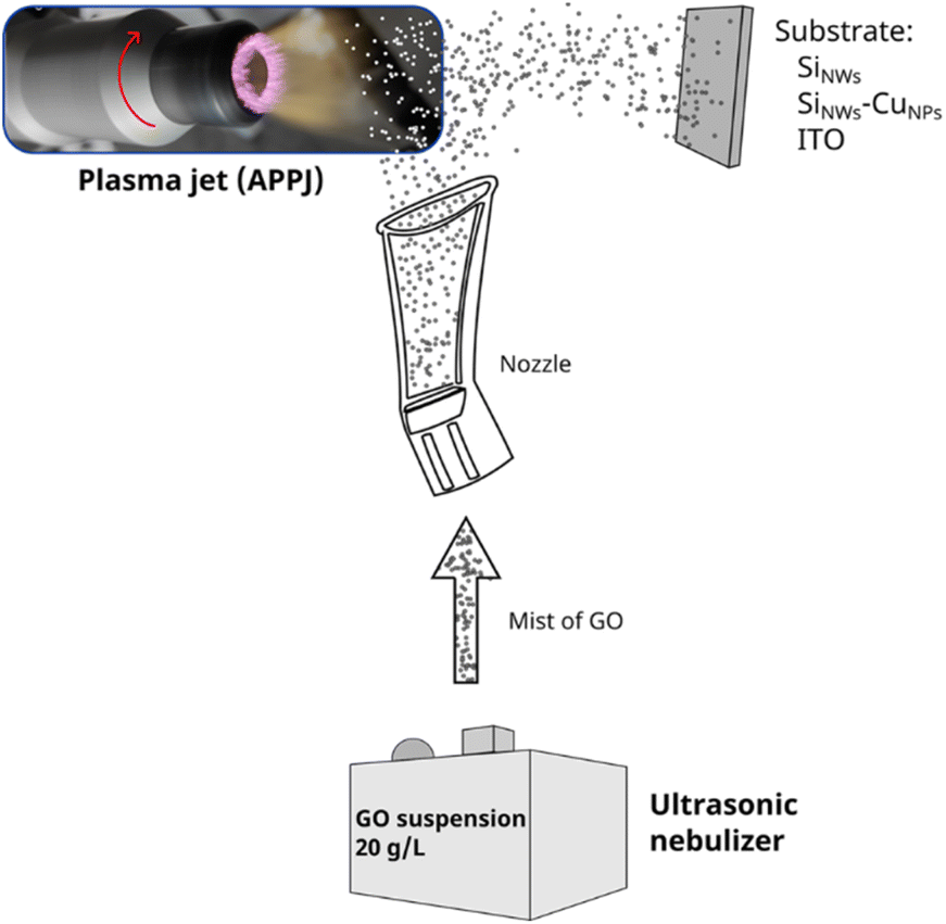 | ||
| Fig. 1 Decoration of the substrates with GO using a plasma system (APPJ). | ||
2.4 Photoelectrocatalytic setup
A three-electrode system was used for the photoelectrochemical experiments. A platinum wire was used as a counter electrode, while a saturated calomel was the reference electrode. Working electrodes were plates of SiNWs, SiNWs-CuNPs, SiNWs-GO, and SiNWs-CuNPs-GO, separately. A 25 mL of 20 ppm methyl orange (MO) solution containing 0.5 M K2SO4 was placed in the cell as an electrolytic solution. The MO solution was purged with N2 gas for 30 min to eliminate the remaining dissolved oxygen. Then, a current of 5 mA was applied to the system for 25 min. A sample of the solution was taken and analyzed by UV-vis spectroscopy. The light source was a LED lamp with a power of 328 W m−2. In dark conditions, the lamp was removed. The evolution of methyl orange concentration was followed by UV-vis Shimadzu UV-2600 equipment. The control sample for light conditions was mounted as described above but omitting the presence of any electrodes. Concerning dark conditions, the control was similar to the light conditions but without the LED lamp or any catalysts. The removal percentage (R) of MO was calculated based on eqn (1):
 | (1) |
2.5 Characterization of samples
Optical Digital Microscopy (Keyence VHX-5000x digital microscope) was used to observe the morphology of the obtained SiNWs. The morphology of all silicon nanowire samples was studied by Scanning Electron Microscopy (SEM). Energy Dispersive X-Ray Spectroscopy (EDS) was also used for the elemental analysis of all catalytic samples. SEM images and EDS analysis were obtained by JEOL JSM-6510LV scanning electron microscope. The crystalline structure of the samples was also determined by X-Ray diffraction (XRD) using a Bruker D8 Advance Diffractometer (Cu-Kα, λα = 1.5406 Å).The samples were analyzed with a HORIBA LabRam micro-Raman spectrometer, model HR800. The laser line used was 532 nm with a nominal power of 73.9 mW.47
The composition of the samples was analyzed by XPS using a Thermo Scientific K-Alpha+ spectrometer. The x-ray source line was Al Kα (hν = 1486.6 eV). The internal pressure in the chamber was about 10−9 mBar and the spot size of about 400 μm. The step energy was 20.0 eV, with ten scans and an initial erosion of 15 s to reduce absorbed atmospheric compounds.
3. Results and discussion
3.1 Characterization of silicon nanowires decorated with copper and GO
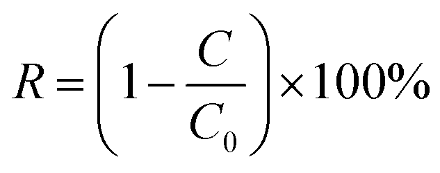
The obtained nanostructures were first observed by digital optical microscopy, where the morphology corresponds to silicon nanowire structures (Fig. 2). The cross-cut view of the silicon substrate containing SiNWs shows the vertically aligned structures and individual SiNWs at the edges of the plate. The average length of the obtained SiNWs was about 52 μm. Agglomerations or bundles were also observed at the tips of the silicon nanowires, which can be associated with van der Waals forces during the drying process.48 The micrograph also revealed a homogeneous distribution of the SiNWs on monocrystalline silicon. This means that the MACE process successfully allowed the production of vertically aligned silicon nanowires.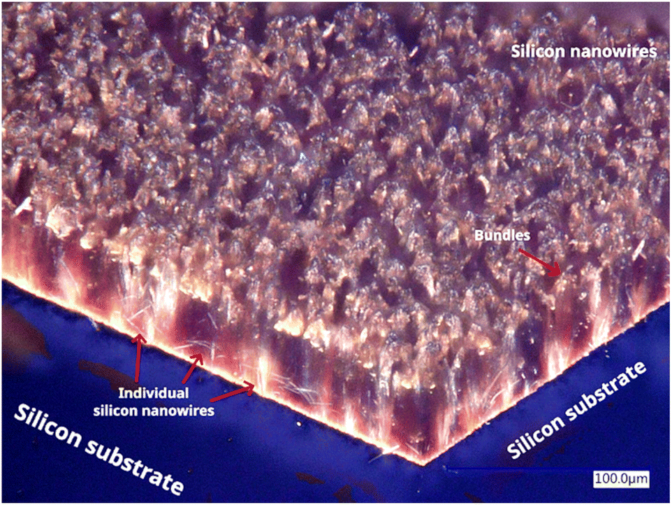 | ||
| Fig. 2 Micrograph isometric view of silicon substrate containing SiNWs obtained by Digital Optical Microscopy. | ||
Fig. 3 shows an image of digital optical microscopy using 2000× for a GO coating on a flat glass slide surface using a deposition time of 2 min. The coating is continuous, with characteristic topography and iridescence caused by light interference within the layer. In this case, the thickness was about 1 μm. The coatings deposited on the SiNWs were thinner since they had lower exposure time to the plasma jet. The GO coatings with 15 s, 30 s, and 60 s of deposition time could have thicknesses on flat surfaces of about 125 nm, 250 nm, and 500 nm, respectively.
 | ||
| Fig. 3 Optical micrograph at 2000× of the GO coating on glass generated by APPJ using 2 min of deposition time. There is a continuous layer with iridescence caused by light interference in the coating. The profile shows a thickness of about 1 μm. | ||
The novelty of this coating yields the assembly of GO flakes of different sizes into a single continuous coating of graphitic structure. In addition, the plasma jet could unbind the hydrogen of the OH functional groups around the GO particles allowing them to bond with each other. This could be attained horizontally to cover the surface and vertically to increase the thickness of the coating.
Fig. 4 shows nine images of digital optical microscopy corresponding to three different views for three sets of samples with 15, 30, and 60 s of deposition time. The GO flakes in the aqueous solution mist went through the plasma jet to generate a single envelope that wrapped the SiNWs bundles. The cross-cut view, the top view, and the border between the SiNWs and crystalline silicon (c-Si) are shown in each row, respectively. The columns correspond to SiNWs-GO for the three deposition times.
 | ||
| Fig. 4 Three different views for three sets of samples with 15 (a–c), 30 (d–f), and 60 (g–i) s of deposition time with the plasma jet for generating a GO envelope that wrapped the SiNWs bundles. The cross-cut view, the top view, and the border between the SiNWs and c-Si are shown in each row, respectively. The columns correspond to SiNWs-GO for the three deposition times. | ||
The GO layer on the SiNWS was around the bundles and not directly on top of the structure. The thicker layers made the SiNWs structures darker but kept the open spaces. Access to inner surfaces was possible only in open spaces, not bundles. This was observed in the cross-cut views (Fig. 4 a, d and g).
Plates of SiNWs, SiNWs-CuNPs, SiNWs-GO, and SiNWs-CuNPs-GO were prepared and analyzed by SEM. Fig. 5 shows the as-obtained vertical structures, consistent with the results offered by other authors and interesting due to their capacity for light trapping, reducing light reflection, and catalytic activity.49–51 As expected, the remaining silver can be observed at the bottom of silicon nanowires due to the MACE process (Fig. 5a–h). According to the elemental mapping of the samples (Fig. 5b, d, f, and h), the silver was located mainly at the bottom of each silicon nanowire sample. Porous structures along silicon nanowires and, in some cases, silver clusters were obtained and attributed to additional etching routes through secondary nucleation of silver nanoparticles.52 Copper was located at the tip of SiNWs-CuNPs, as expected (Fig. S3†), and oxygen was found along nanowires and at the tips, which may indicate the presence of copper oxide. Oxygen was also found distributed over the nanostructures, which is consistent readily with the oxidation of the silicon samples.
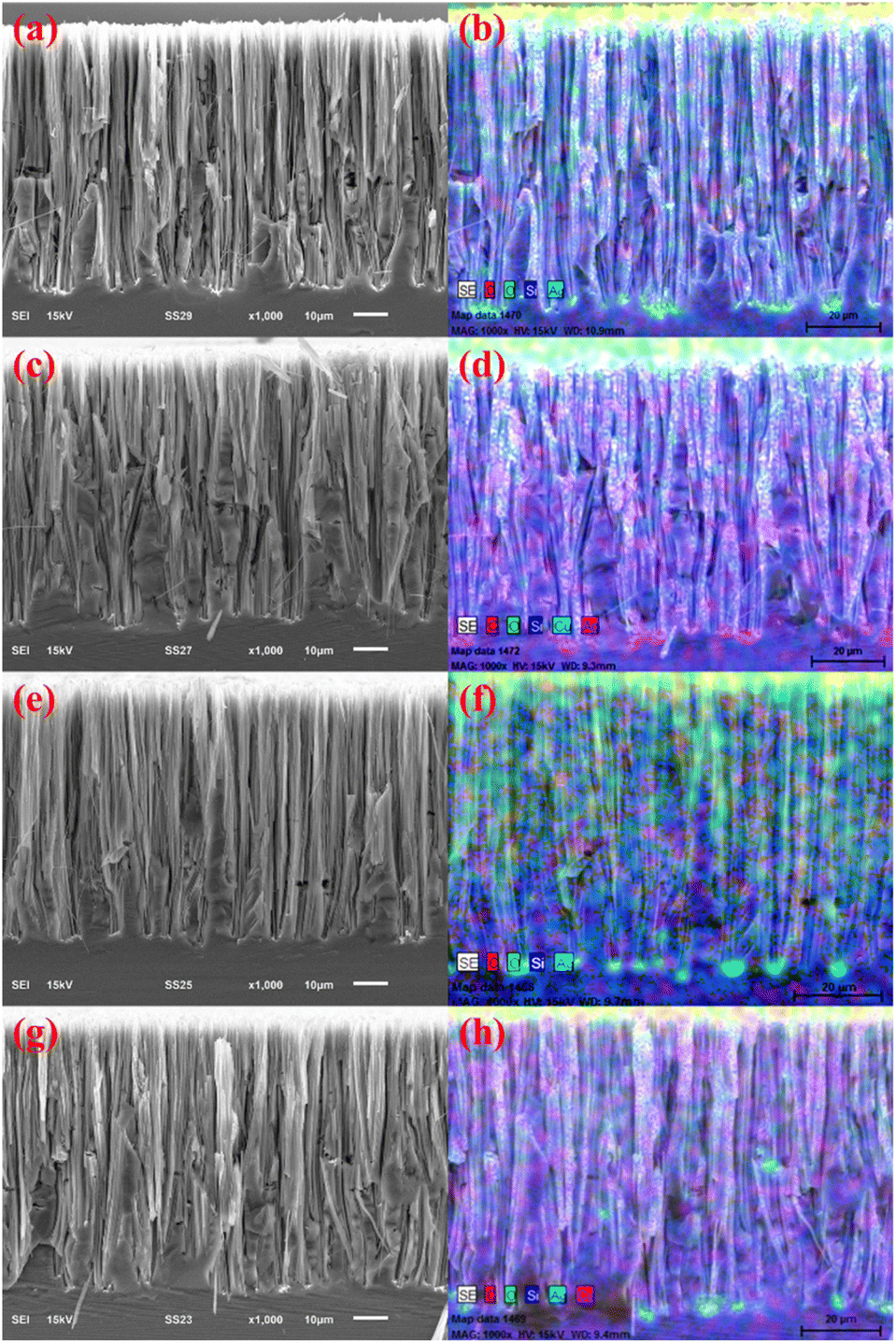 | ||
| Fig. 5 SEM and EDS micrographs of (a)–(b) SiNWs, (c)–(d) SiNWs-CuNPs, (e)–(f) SiNWs-GO, and (g)–(h) SiNWs-CuNPs -GO. The EDS mapping uses a color code for C (red), O (green), Si (blue), Ag (cyan), and Cu (pink), except for incise (d), where Ag and Cu interchanged colors. | ||
On the other hand, copper was scarcely found in the SiNWs-CuNPs-GO sample, probably due to the plasma flow exposure. Therefore, a sample of SiNWs-CuNPs-GO with 1 min of GO deposition time was prepared to compare the remaining copper on the samples (Fig. S6†). Comparing samples in which copper was added (SiNWs-CuNPs, SiNWs-CuNPs-GO with 1 min of GO deposition time, and SiNWs-CuNPs-GO with 2 min of GO deposition time), the amount of copper was lower in the samples containing GO. According to the semi-quantitative analysis shown in Fig. S3, S5, and S6,† the weight percentage of copper decreased from 1.28% in the SiNWs-CuNPs sample to 0.87% in the SiNWs-CuNPs-GO sample for 1 min deposition time in comparison to a lower amount of 0.38% in the SiNWs-CuNPs-GO sample with 2 min deposition time. During the deposition of GO, the air/plasma flow probably dragged out most of the copper nanoparticles attached at the tips of silicon nanowires. Such CuNPs detachment was not previously seen in any test or treatment. However, some deposited copper nanoparticles could remain attached to the nanowires, which could be enough to exhibit catalytic activity. This means that the exposure time to the plasma flow could be a critical parameter for the quantity of material deposited and the composition of the original sample.
Samples of c-Si (i.e., a silicon plate without nanowires or treatment), SiNWs, and SiNWs-CuNPs were analyzed by X-ray diffraction technique (Fig. 6). All the samples showed the silicon response for (111) planes, which has been observed in vertical silicon nanowires.48 Furthermore, silver peaks were detected in both SiNWs and SiNWs-CuNPs samples. This implies that metallic nanoparticles are located at the bottom of nanostructures, as seen in SEM. Regarding SiNWs-CuNPs, copper and copper(I) oxide peaks were detected in this sample. This confirms the correct attachment of copper nanoparticles by the experimental method used. Furthermore, the peaks of copper oxide in Fig. 6 indicate the presence of copper oxide besides the metallic copper nanoparticles. Hence, copper nanoparticles and copper(I) oxide were obtained at the tips of the SiNWs-CuNPs samples.
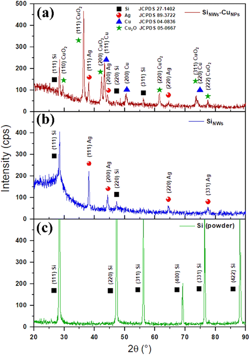 | ||
| Fig. 6 XRD analyses for (a) SiNWs-CuNPs, (b) SiNWs, and (c) c-Si samples. | ||
3.2 Electrochemical response of deposited GO on ITO
Deposited GO on ITO was first examined by cyclic voltammetry (Fig. 7). Compared with the bare ITO plate, the typical response of carbon materials was obtained. In the first cycle of the anodic direction, there were no peaks of any oxidation process in the window 0.5–1.0 V. This is expected for an oxidized material such as GO. As the cycle goes in the cathodic direction, reduction processes occur and oxidation peaks appear while returning to the anodic direction (peak i). During the cyclic scanning, the evolution of a redox pair (peaks ii and iii) was observed, which is associated with quinone/hydroquinone conversion.53,54 The peak i has been reported in the graphene production from graphitic materials. It is related to the intercalation of ions containing sulfur functional groups,55,56 which could be associated with sulfate ions from sulfuric acid and potassium sulfate.57,58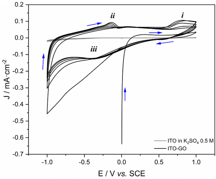 | ||
| Fig. 7 Cyclic voltammetry of GO deposited on ITO surface. Arrows indicate the direction of cycles. Supporting electrolyte: K2SO4 0.5 M; v = 20 mV s−1. | ||
The nature of the deposited carbon material was also investigated through the chronoamperometry technique. As shown in Fig. 7, there was no oxidation peak at the potential 0.8 V in the first cycle. On the other hand, from the second cycle, there was a notable formation of peak iii. For this reason, the chronoamperometric experiments were performed by applying 0.8 and −0.4 V vs. SCE for 10 min in two different fresh samples of ITO covered with GO (deposition time: 2 min, Fig. 8). The observed evolution of the current while applying −0.4 V (Fig. 8a) can be associated to the peak iii and fitted to the Cottrell's model. This means that there is a process controlled by diffusion and, therefore, can be related to an electrochemically reducible material on the surface of ITO.
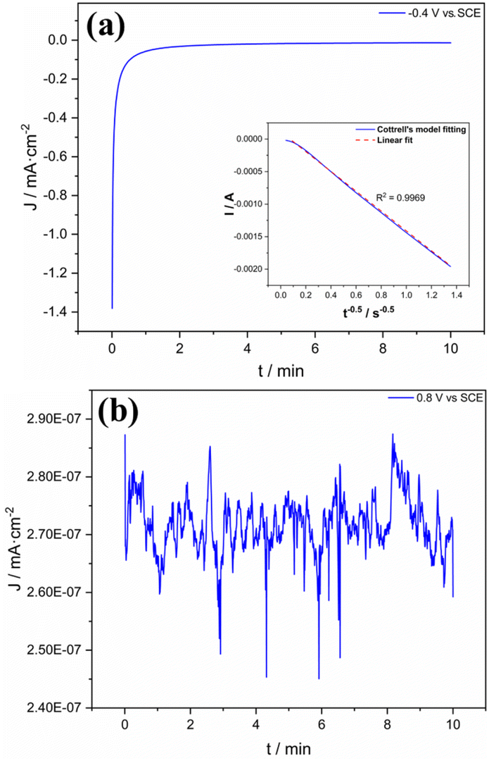 | ||
| Fig. 8 Chronoamperometric measurements of GO deposited on ITO at (a) −0.4 V and (b) 0.8 V vs. SCE during 10 min; inset: data adjusted to Cottrell's model. The supporting electrolyte was K2SO4 0.5 M. | ||
Regarding the imposition of 0.8 V (Fig. 8b), no significant current was obtained in this case. This behavior was maintained during the whole time of the imposition of potential. It fits with the observation at the same potential for the first cycle in Fig. 7. The fresh ITO-GO sample possesses an oxidized material, which can no longer be oxidized at 0.8 V without the imposition of a reduction process. The presence of oxidized species can explain the very small current obtained. Therefore, the evidence indicates the presence of oxidized carbon material on the surface of ITO and can be associated to GO.
3.3 Electrochemical behavior of silicon nanowires decorated with copper and GO
The surfaces of SiNWs and SiNWs-CuNPs decorated with GO were investigated electrochemically and compared with their bare counterparts (Fig. 9). The electrochemical response for SiNWs-CuNPs-GO was higher compared to SiNWs-CuNPs. The increased current was also obtained in the cathodic window −1.0 to −0.25 V, similar to the response obtained with ITO-GO (Fig. 7). Regarding SiNWs-GO (Fig. 9, inset), the response was also higher as compared to SiNWs. In the anodic window of 0.0–1.0 V, an oxidation current was observed in SiNWs, but only a capacitive current was found on SiNWs-GO. This effect can be due to the coverage of silicon nanowires with GO.37 In the cathodic window of −1.0 to −0.25 V, the response of GO in SiNWs-GO was obtained and only capacitive current for SiNWs was present. The improvement of the current response of SiNWs-CuNPs can be attributed to the presence of the more conductive copper, while the enhancement in SiNWs-CuNPs-GO can be associated with the particles of GO.59,60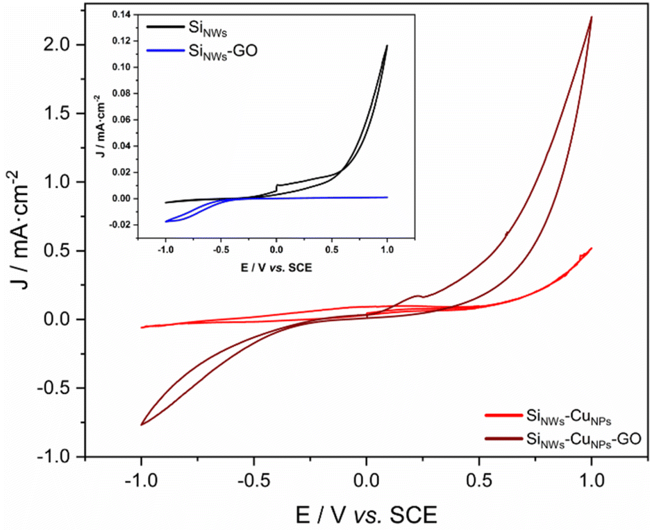 | ||
| Fig. 9 Cyclic voltammetry of SiNWs-CuNPs and SiNWs-CuNPs decorated with GO. Inset: cyclic voltammetry of SiNWs and SiNWs-GO. Supporting electrolyte: K2SO4 0.5 M; v = 20 mV s−1. | ||
3.4 Characterization of silicon nanowires after electrochemical tests
Samples of SiNWs-GO and SiNWs-CuNPs-GO were analyzed by XPS (Fig. 10a–g). An additional SiNWs-CuNPs-GO sample was treated with several cyclic scans to obtain the electrochemical response of GO over the SiNWs-CuNPs. After the treatment, the remaining sample was also analyzed by XPS (Fig. 10h–k). Deconvolution of the signals of the samples was done using the Gaussian model. All the samples showed the presence of C–C/C–H bonds (284.7, 284.8 eV) as well as C–O–H/C–OH groups (286.51, 286.23 eV), indicating the presence of typical functional groups of GO.61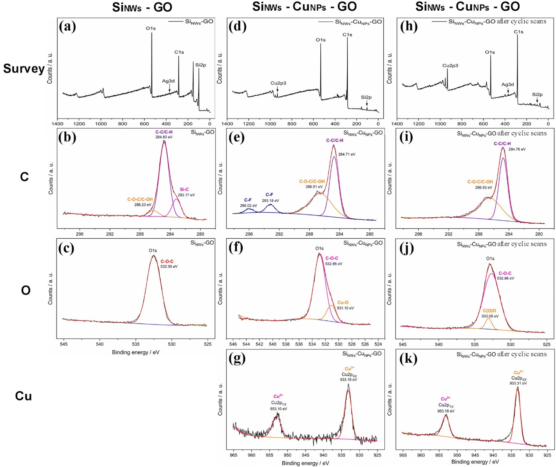 | ||
| Fig. 10 XPS analysis of samples (a) SiNWs-GO, (d) SiNWs-CuNPs-GO, and (h) SiNWs-CuNPs-GO after cyclic scans (surveys); (b, e and i) carbon deconvolution for the samples; (c, f and j) oxygen deconvolution; (g and k) copper deconvolution. | ||
The signals for C–F bonds (293.18, 296.02 eV) were also found,62 which can be related to the silicon nanowires etching process due to the solutions containing HF. Besides, oxygen deconvolution corresponds to the C–O–C bond (532.86, 532.5 eV). Also, the Cu–O bond (531.1 eV) was found in the SiNWs-CuNPs-GO sample. In the SiNWs-CuNPs-GO sample, after cyclic scans, signals were found for the C–O–C bond (532.66 eV) and C(O)O (533.08 eV). This is also in agreement with the Cu2+ signals deconvoluted for both SiNWs-CuNPs-GO (933.18, 953.1 eV) and SiNWs-CuNPs-GO after cyclic scans (933.31 eV, 953.18 eV) of the samples.63,64 The presence of copper(II) oxide is consistent with the production of this oxide during the exposition of the samples to the plasma flow39,65 for the deposition of GO. No other significant differences were found between the samples containing copper. These results indicate the presence of oxygen-carbon functional groups associated with GO in the samples and copper(II) oxide in the SiNWs-CuNPs-GO sample, as was also found by X-Ray diffraction analysis.
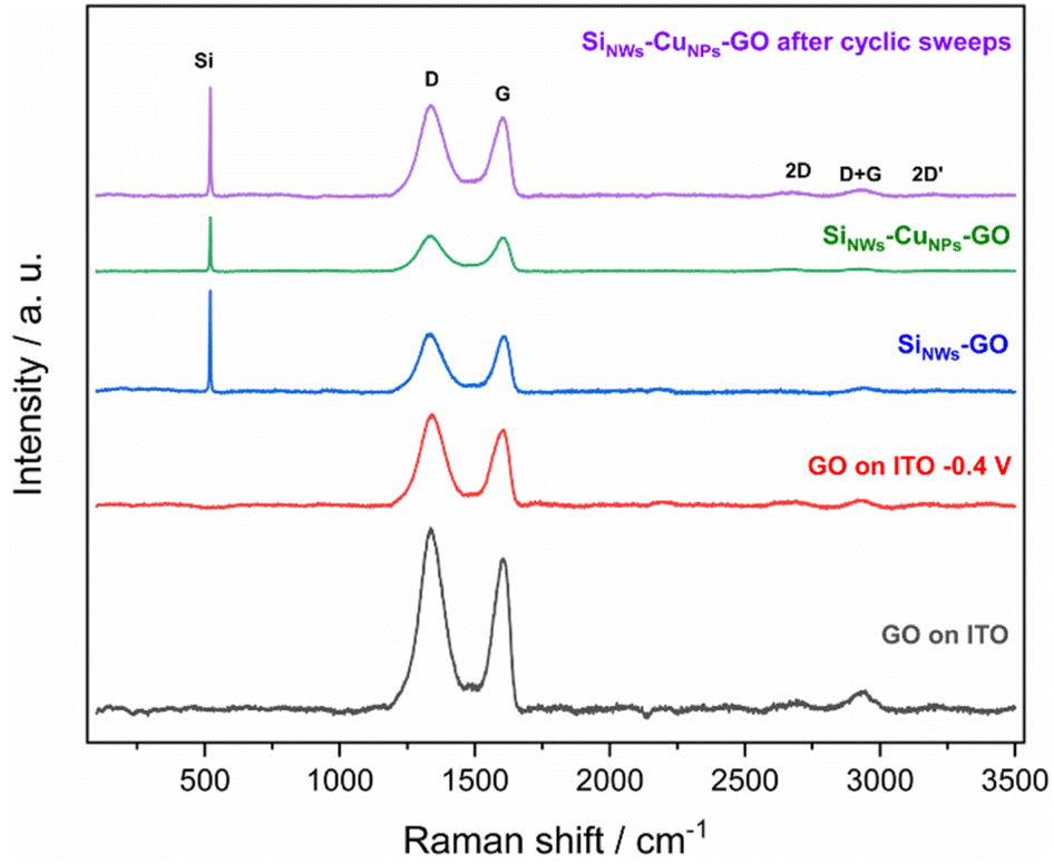
Surfaces containing deposits of GO were studied by Raman analysis (Fig. 11). Deposits were obtained on the surface of ITO (deposition time: 2 min) compared to silicon nanowires substrate. A potential of −0.4 V vs. SCE was applied in a GO sample over ITO to investigate the possible changes in the sample in the process of getting an electrochemically reduced sample of GO. In the same way, several cyclic scans were applied to a SiNWs-CuNPs-GO sample to obtain the electrochemical response of GO over the SiNWs-CuNPs. The samples were then analyzed by Raman spectroscopy to obtain evidence of the presence of GO. As is shown in Fig. 11, the presence of GO was confirmed in all the samples, and a peak corresponding to Si (520 cm−1) was detected in the silicon nanowires samples.66,67 The D band, located at 1319–1346 cm−1 corresponds to the presence of defects in the hexagonal structure of the graphene, while the G band (graphitic, located at 1576–1580 cm−1) is associated with the sp2 carbon structures. The 2D band stands for the coherent double resonant process and is an indicator of the graphene layers in the sample.9,30,31
 | ||
| Fig. 11 Raman spectra of ITO covered with GO, SiNWs-GO, SiNWs-CuNPs-GO, and SiNWs-CuNPs-GO after cyclic scans. | ||
The D + G and 2D′ bands were also found at 2840 and 3120 cm−1, respectively, which is a characteristic signature marker of GO.66 A strong D peak and a moderate 2D band were observed in all cases, which implies defects, edges, or multilayer graphene structures.32 Since the comparative sample (GO on ITO) showed defects within the GO structure, it is challenging to identify changes in the samples exposed to cyclic scans and −0.4 V (the potential applied to produce reduced GO). Reduced GO is usually made in strong conditions, such as acidic media and using several cyclic scans,61 which was not the case in this work. The ratio of intensities of D and G peaks (ID/IG) is used as an indicator of defects in the deposits of GO. A higher ratio is expected for reduced GO than the original sample of GO due to the introduction of defects within the structure caused by the elimination of oxygen functional groups and the loss of carbon atoms.9,10,34,38 Because the D peak was higher than G, it is not possible to conclude the presence of reduced GO in the samples caused by the cyclic scans and applying −0.4 V. After photoelectrocatalytic tests, as shown in the following section, the system did not have the conditions to reduce GO, neither the potential nor the time to accomplish significant reduction of GO. Nevertheless, the characteristic bands of GO on all the samples are enough to conclude its presence in the silicon nanowires and ITO. Hence, the successful deposition of GO was achieved.
3.5 Photoelectrocatalytic activity of silicon nanostructures
Photoelectrocatalytic activity of as-prepared SiNWs, SiNWs-CuNPs, SiNWs-GO, and SiNWs-CuNPs-GO have been probed using MO, promoting its remotion under visible light. Fig. 12a shows the typical UV-vis spectra of MO and its characteristic peak at 465 nm.1,68 The intensity of this peak was used for monitoring the remaining amount of MO in the solution over time. The continuous decrease in the MO peak intensity suggests the remotion of the dye over the surfaces of nanostructured catalysts. This behavior was observed in all silicon nanostructures used, but the degree of remotion found was different between them. The remotion of MO was also studied in the absence of light, as can be observed in Fig. 12c and d. The ratio of the initial concentration of MO (C0) to the concentration during the experiment (C) C/C0 was very low in the controls, which consisted of the solution without any catalyst. This implies the absence of self-degradation of MO under light and dark conditions.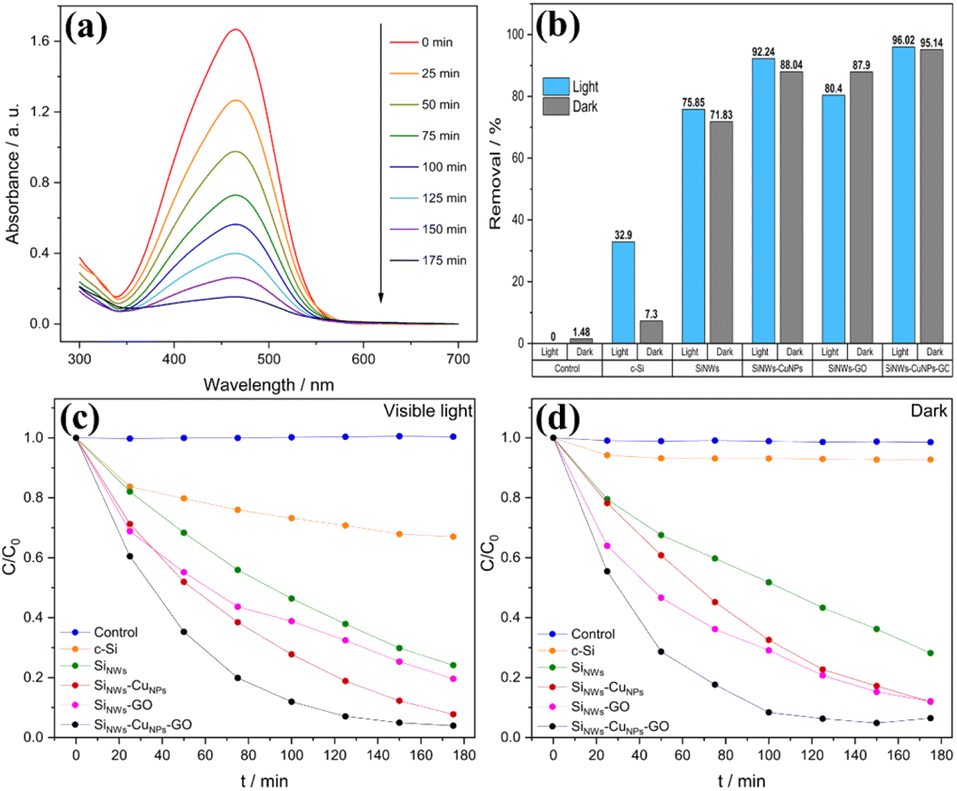 | ||
| Fig. 12 (a) UV-vis spectra of MO samples during the experimentation time; (b) removal percentage of MO using the photocatalyst proposed in dark and light; (c) evolution of MO concentration over time in the presence of visible light and (d) dark using c-Si, SiNWs, SiNW-CuNPs, SiNWs-GO, and SiNWs-CuNPs-GO as photocatalysts. | ||
In the presence of c-Si, the remotion of the dye was distinctive compared to the controls in both light and dark. In the absence of nanostructures, the remotion of the dye was poor, and due to photolysis, only 32.9% of the original dye in the solution could be removed. In general, SiNWs exhibited a higher remotion capacity than the c-Si and the decorated SiNWs with copper and/or GO showed higher removal capacity than bare SiNWs. The remotion obtained with SiNWs was 75.85% under light conditions compared to 71.83% in the dark, while the removal using SiNWs-CuNPs was 92.24% in light and 88.04% in the dark (Fig. 10h). The enhanced remotion capacity can be explained by the presence of metallic nanoparticles on the surface of silicon nanowires (CuNPs) that increases the electronic transfer and hence improve the catalytic activity during the photoelectrocatalytic process.69
The photocatalytic activity of semiconductor–metal catalyst mainly depends on the electron work function of the metal, and it is a significant parameter involved in the electronic transfer from the conduction band in the semiconductor to the metal.69,70 In the presence of light, the remotion was higher than in the dark, as expected due to the photocatalytic properties of silicon nanowires, which capture light and promote the separation of electron–hole pairs.73 Moreover, in the presence of GO, the nanostructures showed a contrary effect in SiNWs-GO. Although the remotion efficiency obtained with SiNWs-GO (80.4% in light, 87.9% in the dark) was superior to SiNWs in both light and dark conditions (75.85% in light, 71.83% in the dark), as shown in Fig. 12b, it was found that in the dark the remotion was higher than in light. This seems contradictory to the literature, which indicates that the GO on the surface of SiNWs can increase catalytic activity31–33,74 besides light trapping and carrier generation. Regarding the SiNWs-CuNPs-GO photocatalyst, a similar removal percentage was found in light and dark conditions (96.02% and 95.14%, respectively). These values are enhanced as compared to SiNWs-CuNPs (92.24% in light and 88.04% in the dark). In general, the presence of copper nanoparticles led to more remotion capacity of SiNWs, and better dye discoloration was observed when decorating SiNWs with both copper nanoparticles and GO. Compared with data reported by other authors (Table 1), without considering specific test parameter values, a competitive removal capacity of SiNWs-CuNPs-GO can be achieved within a few hours of photoelectrocatalytic activity.
| Photocatalyst structure | Target molecule | Degradation or removal efficiency | Ref. |
|---|---|---|---|
| SiNWs-AgNPs | Methylene blue | 98–99% (200 min) | 70 |
| Hydrogen-terminated SiNWs | Methylene blue (4 mL, 10−6 M) | 83.32% (200 min) | 48 |
| Methyl orange (4 mL, 10−6 M) | 93% (200 min) | ||
| SiNWs–AuNPs | Rhodamine B (3 mL, 5 × 10⁻⁶ M) | 80% (240 min) | 71 |
| SiNWs decorated with Pd | Methyl orange (260 mL, 25 mg L−1) | 84.5% (microbial fuel cell, 36 h) | 72 |
| SiNWs-rGO | Indigo carmine (0.1 M) | > 99% (105 min) | 37 |
| SiNWs-rGO-CuO | Ciprofloxain (4 mL, 10 mg L−1) | 95.78% (in 0.6 mM PMS, 40 min) | 10 |
| SiNWs-GO | Methylene blue (200 mL, 6.4 mg L−1) | 93% (280 min); 96% (in H2O2, 120 min) | 9 |
| SiNWs-CuNPs-GO | Methyl orange (25 mL, 20 mg L−1, 175 min of photoelectrocatalysis) | 96.02% in light, 95.14% in dark | This work |
| SiNWs-CuNPs | 92.24% in light, 88.04% in dark | ||
| SiNWs-GO | 80.4% in light, 87.9% in dark | ||
| SiNWs | 75.85% in light, 71.83% in dark | ||
| c-Si | 32.9% in light, 7.3% in dark |
The apparent rate constant also reflected the enhanced capacity of MO removal as promoted by copper and GO. The data of concentration ratio C/C0 was adjusted to the simplified Langmuir–Hinshelwood kinetics model as shown in eqn (2):75
ln![[thin space (1/6-em)]](https://www.rsc.org/images/entities/char_2009.gif) C = −krkat + lnC0 = −kt + lnC0 C = −krkat + lnC0 = −kt + lnC0
| (2) |
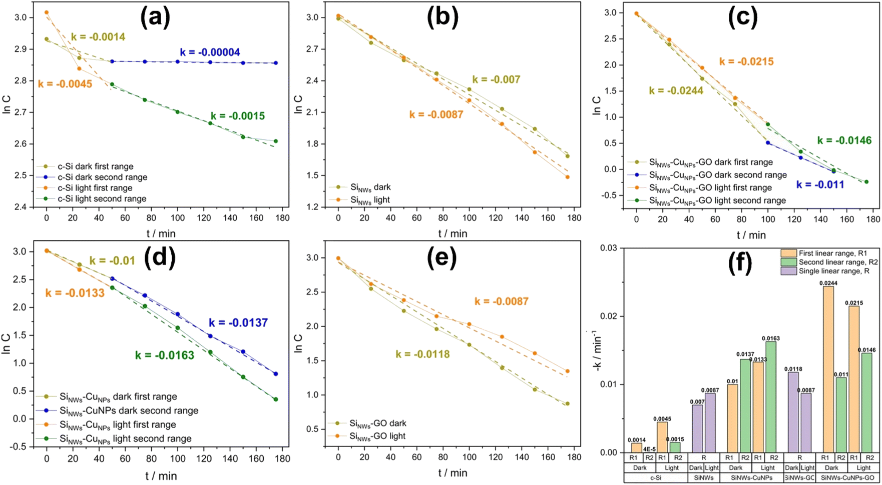 | ||
| Fig. 13 Kinetics for MO remotion using (a) c-Si, (b) SiNWs, (c) SiNWs-CuNPs-GO, (d) SiNW–CuNPs, (e) SiNWs-GO, and as photocatalysts. (f) Comparison for all rate constants found using the photocatalyst proposed. | ||
As expected, the lower values for rate constant were found with c-Si due to the absence of nanostructures capable of adsorbing and catalyzing the remotion of the dye. On the other hand, the rate constants found in SiNWs and SiNWs-CuNPs photocatalysts were higher in the presence of light, in agreement with the removal percentage discussed above and with the photocatalytic properties of silicon nanowires. Nevertheless, the rate constant values for SiNWs-GO and SiNWs-CuNPs-GO found were slightly higher in the dark. This is because the amount of GO deposited on the SiNWs surface can influence the performance of the catalytic activity of materials. The presence of GO makes the electron transfer faster between SiNWs and GO as well as SiNWs-CuNPs and GO. However, when the amount of GO particles on the surface is large enough, the thickness of the GO layer and its associated series resistance can increase.36 This can reduce the catalytic activity of the substrate and hence lower its removal capacity.
GO has valence and conduction band potentials of about 2.787 and −0.323 eV vs. NHE, respectively (Fig. 14).76,77 These values are very near to the values of TiO2, which is a predominantly oxidizing photocatalyst, while Cu2O is a reducing one. The SiNWs structures are excellent in absorbing illumination and generating electron–hole pairs and they can be benefited by allocating Cu2O and GO or TiO2. In Z-scheme configurations, GO has also been applied as an electron receptor generated by the SiNWs by transferring them to the surface and protecting the SiNWs.9
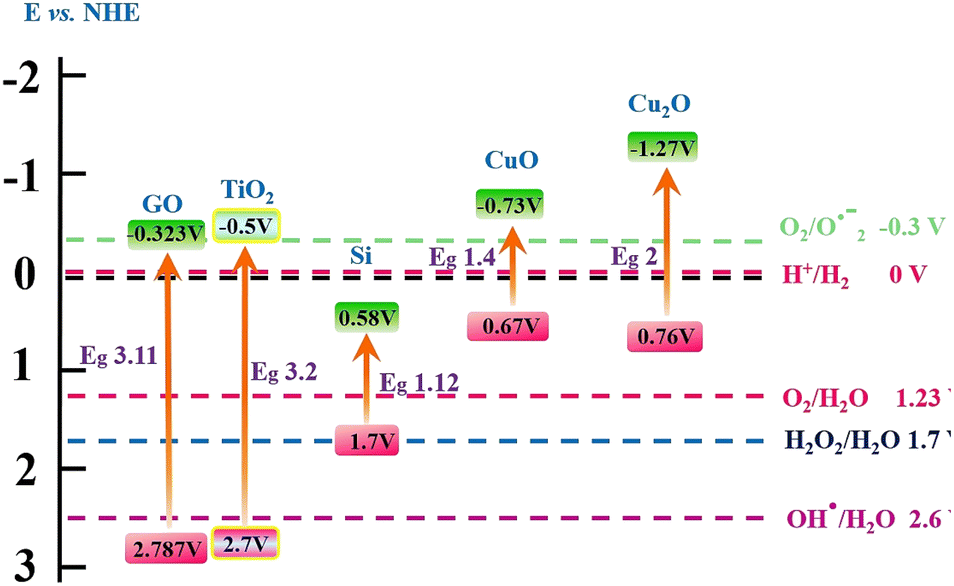 | ||
| Fig. 14 Band gap, conduction band and valence band electrochemical potentials influence the mechanisms for making the photocatalytic processes efficient in the SiNWs, SiNWs-CuNPs, and SiNWs-CuNPs-GO. TiO2 was included for comparison. | ||
Based on the evidence provided by the different photocatalysts employed in this work and, accordingly with the observations of other authors, the enhancement of catalytic activity is mainly related to electron–hole pair separation and faster carrier transport. When the different photocatalysts are irradiated with visible light while a current is applied to the system, the photoexcitation produces the separation of electron–hole pairs. After the separation, some of the generated charge carriers are discharged on the surface of the SiNWs. In the case of SiNW–CuNPs, the generated electrons in the conduction band (CB) of SiNWs migrate to the CB of CuNPs while the holes are transported from the valence band (VB) of CuNPs to the VB of SiNWs and then to the anode. Similar dynamics of SiNWs-CuNPs can be expected for the SiNWs-GO catalyst, where the GO can facilitate the charge separation and transport electrons from SiNWs to GO. Furthermore, the Ag nanoparticles could promote electron discharge to generate reactive oxygen species contributing to dye bleaching.
Regarding the SiNWs-CuNPs-GO substrate, the generated electrons are transported from SiNWs through CuNPs and discharged to GO.75,78,79 There has also been proposed a Z-scheme system for SiNWs-CuNPs-GO, where the photogenerated electrons in the CB of CuNPs can react with the holes in the VB of SiNWs through GO while the electrons in the CB of SiNWs are transferred onto GO and then discharged to the electrolyte.10 Once the carriers reach the photocatalyst–electrolyte interface, they can react with water and dissolved oxygen to produce reactive oxygen species (ROS). In addition, the ROS produced at the surface of the catalytic materials, such as ˙OH and O2−, can lead to the oxidation of the dye. These processes are schematically represented in Fig. 15 for clear comprehension.
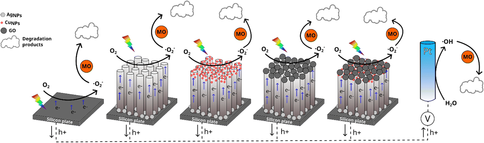 | ||
| Fig. 15 Schematic illustration of the possible MO photoelectrocatalytic degradation/removal mechanism using c-Si, SiNWs, SiNWs-CuNPs, and SiNWs-CuNPs-GO. Dashed lines represent the possible connection to the platinum counter electrode. | ||
4. Conclusion
The SiNWs and SiNWs-CuNPs were prepared by the metal-assisted chemical etching method (MACE). The EDS, XRD, and XPS analysis confirmed the composition of the photoelectrocatalysts, thus confirming the presence of silver at the bottom of the silicon nanowires and the copper and copper(I) oxide attached at the tips of the SiNWs-CuNPs. In addition, copper(II) oxide was found on the samples exposed to the plasma.The presence of GO on the surface of SiNWs-GO and SiNWs-CuNPs-GO, as confirmed by Raman spectroscopy, corroborates that the samples are well covered with GO using the plasma deposition method.
The novelty of the GO coating is in the assembly of GO flakes of different sizes into a single continuous coating of graphitic structure. Furthermore, the plasma jet could unbind the hydrogen of the OH functional groups around the GO particles, subsequently allowing them to bond with each other. This could be attained horizontally to cover the surface and vertically to thicken the coating.
The heterostructures were tested using MO as a probe molecule, thus leading to its excellent removal (96.02% in 175 min) with SiNWs-CuNPs-GO photocatalyst (light conditions), followed by the same photocatalyst in the dark (95.14%), SiNWs-CuNPs (92.24% in light, 88.04% in the dark), SiNWs-GO (80.4% in light, 87.9% in the dark), SiNWs (75.85% in light, 71.83% in the dark), and c-Si (32.9% in light, 7.3% in the dark).
The enhanced photoelectrocatalytic properties of SiNWs-CuNPs-GO were also evidenced in the rate constant, which was the highest compared with the other photocatalysts tested in this work.
The remotion efficiency obtained with SiNWs-GO (80.4% in light, 87.9% in the dark) was superior to SiNWs in both light and dark conditions (75.85% in light, 71.83% in the dark). However, the remotion was higher for SiNWs-GO in the dark than in light.
The proposed method for obtaining GO deposits is not limited to silicon substrate but to other surface kinds where the GO may improve the properties of the studied materials.
Author contributions
Carlos Hernández Rodríguez: conceptualization, methodology, investigation, validation, supervision, writing–original draft, writing–review & editing. José de Jesús Pérez Bueno: conceptualization, methodology, investigation, validation, funding acquisition, supervision, writing–original draft, writing–review & editing. Alejandra Xochitl Maldonado Pérez: methodology, assisted with experiments, investigation, writing–review & editing. Missael Ruiz Flores: methodology, investigation, assisted with experiments. Goldie Oza: conceptualization, methodology, investigation, validation, funding acquisition, supervision, writing–review & editing.Conflicts of interest
There are no conflicts to declare.Acknowledgements
This work was funded by the National Council of Science and Technology CONACYT (México) through the Basic and/or Frontier Science grant no. 320114; the funding from the National Laboratory of Graphene Materials and the LANIAUTO is greatly appreciated. Furthermore, the authors appreciate the support of the “Fondo Sectorial CONACYT-SENER Sustentabilidad Energética” through grant 207450, “Centro Mexicano de Innovación en Energía Solar (CeMIESol)”, within strategic project no. P62, “Prototype hybrid system of a supercritical CO2 expander with flat polycarbonate mirrors on automated heliostats”. Further, the authors thank The World Bank and SENER, who supported this work through grant no. 002/2017-PRODETES-PLATA. The authors also thank Ciencia de Fronteras Project from CONACYT (grant no. CF-19/2096029). The authors appreciate the technical assistance of José Germán Flores López in the SEM analyses. Thanks to Dr David Meneses Rodríguez for his contribution to obtaining the XPS analyses. The authors also wish to thank the Center of Nanoscience and Micro and Nanotechnology of the Polytechnic National Institute (CNMN-IPN) and Luis Alberto Moreno Ruíz for the technical assistance in the Raman analysis.References
- S. H. Li, Y. Zhao, J. Chu, W. W. Li, H. Q. Yu and G. Liu, Electrochemical Degradation of Methyl Orange on Pt-Bi/C Nanostructured Electrode by a Square-Wave Potential Method, Electrochim. Acta, 2013, 92, 93–101, DOI:10.1016/j.electacta.2013.01.012.
- C. Jayakrishnan, S. R. Sheeja, J. Duraimurugan, S. Prabhu, R. Ramesh, G. S. Kumar, P. Maadeswaran and M. Shkir, Photoelectrochemical Properties and Photocatalytic Degradation of Methyl Orange Dye by Different ZnO Nanostructures, J. Mater. Sci.: Mater. Electron., 2022, 33, 9732–9742, DOI:10.1007/s10854-022-07801-0.
- W. He, Y. Liu, J. Ye and G. Wang, Electrochemical Degradation of Azo Dye Methyl Orange by Anodic Oxidation on Ti4O7 Electrodes, J. Mater. Sci.: Mater. Electron., 2018, 29, 14065–14072, DOI:10.1007/s10854-018-9538-6.
- W. Zhao, J. Xing, D. Chen and J. Shen, Comparative Studies on the Performance of Porous Ti/Sno2-Sb2O3/Pbo2 Enhanced by CNT and Bi Co-Doped Electrodes for Methyl Orange Oxidation, J. Adv. Oxid. Technol., 2017, 20(1), 20160181, DOI:10.1515/jaots-2016-0181.
- Y. Kong, Z. L. Wang, Y. Wang, J. Yuan and Z. D. Chen, Degradation of Methyl Orange in Artificial Wastewater through Electrochemical Oxidation Using Exfoliated Graphite Electrode, New Carbon Mater., 2011, 26, 459–464, DOI:10.1016/S1872-5805(11)60092-9.
- G. V. Kornienko, T. A. Kenova, V. L. Kornienko, O. A. Golubtsova and N. G. Maksimov, Electrochemical Oxidation of Dyes on Oxide Lead Anode with the Involvement of Active Oxygen Species, Russ. J. Appl. Chem., 2017, 90, 1234–1238, DOI:10.1134/S1070427217080079.
- X. Yu, X. Jin, X. Chen, A. Wang, J. Zhang, J. Zhang, Z. Zhao, M. Gao, L. Razzari and H. Liu, A Microorganism Bred TiO 2/Au/TiO 2 Heterostructure for Whispering Gallery Mode Resonance Assisted Plasmonic Photocatalysis, ACS Nano, 2020, 14, 13876–13885, DOI:10.1021/acsnano.0c06278.
- L. Wang, X. Tang, Z. Yang, J. Guo, Z. You, Y. Cai, X. Niu, X. Zhang, L. Zhang and J. Zhang, et al., Regulation of Functional Groups Enable the Metal-Free PDINH/GO Advisable Antibacterial Photocatalytic Therapy, Chem. Eng. J., 2023, 451, 139007, DOI:10.1016/j.cej.2022.139007.
- M. Gaidi, K. Daoudi, S. Columbus, A. Hajjaji, M. A. E. Khakani and B. Bessais, Enhanced Photocatalytic Activities of Silicon Nanowires/Graphene Oxide Nanocomposite: Effect of Etching Parameters, J. Environ. Sci., 2021, 101, 123–134, DOI:10.1016/j.jes.2020.08.010.
- A. Khen, T. Hadjersi, N. Brihi, F. Moulai, O. Fellahi, S. Naama, M. Ifires and A. Manseri, Preparation of SiNWs/RGO/CuO Nanocomposites as Effective Photocatalyst for Degradation of Ciprofloxacin Assisted with Peroxymonosulfate, J. Inorg. Organomet. Polym. Mater., 2022, 32, 1078–1091, DOI:10.1007/s10904-021-02184-x.
- X.-Q. Bao, D. Y. Petrovykh, P. Alpuim, D. G. Stroppa, N. Guldris, H. Fonseca, M. Costa, J. Gaspar, C. Jin and L. Liu, Amorphous Oxygen-Rich Molybdenum Oxysulfide Decorated p-Type Silicon Microwire Arrays for Efficient Photoelectrochemical Water Reduction, Nano Energy, 2015, 16, 130–142, DOI:10.1016/j.nanoen.2015.06.014.
- N. Y. Labrador, X. Li, Y. Liu, H. Tan, R. Wang, J. T. Koberstein, T. P. Moffat and D. V. Esposito, Enhanced Performance of Si MIS Photocathodes Containing Oxide-Coated Nanoparticle Electrocatalysts, Nano Lett., 2016, 16, 6452–6459, DOI:10.1021/acs.nanolett.6b02909.
- K. Daoudi, M. Gaidi, H. Alawadhi, S. Columbus, D. Zhang, A. Allagui, M. Shameer and A. Taieb, Structural Effects of Silver-Nanoprism-Decorated Si Nanowires on Surface-Enhanced Raman Scattering, Nanotechnology, 2020, 31(25), 255706, DOI:10.1088/1361-6528/ab80fa.
- S. Chakraborti, R. N. Basu and S. K. Panda, Vertically Aligned Silicon Nanowire Array Decorated by Ag or Au Nanoparticles as SERS Substrate for Bio-Molecular Detection, Plasmonics, 2018, 13, 1057–1080 CrossRef CAS.
- S. Rani and A. K. Shukla, Investigation of Silver Decorated Silicon Nanowires as Ultrasensitive and Cost-Effective Surface-Enhanced Raman Substrate, Thin Solid Films, 2021, 723, 138595, DOI:10.1016/j.tsf.2021.138595.
- Y. Xi, W. Zhang, Z. Fan, Q. Ma, S. Wang, D. Ma, Z. Jiang, H. Li and Y. Zhang, A Facile Synthesis of Silicon Nanowires/Micropillars Structure Using Lithography and Metal-Assisted Chemical Etching Method, J. Solid State Chem., 2018, 258, 181–190, DOI:10.1016/j.jssc.2017.07.034.
- N. L. Nguyen, T. C. H. Phan, T. M. D. Dang and M. C. Dang, Formation of Silver Nanoparticles and Their Application for Suppressing Surface Reflection of N-Type Silicon, Adv. Nat. Sci.: Nanosci. Nanotechnol., 2019, 10(2), 025014, DOI:10.1088/2043-6254/ab1cb3.
- O. Fellahi, A. Barras, G.-H. Pan, Y. Coffinier, T. Hadjersi, M. Maamache, S. Szunerits and R. Boukherroub, Reduction of Cr(VI) to Cr(III) Using Silicon Nanowire Arrays under Visible Light Irradiation, J. Hazard. Mater., 2016, 304, 441–447, DOI:10.1016/j.jhazmat.2015.11.020.
- C. Huo, J. Wang, H. Fu, X. Li, Y. Yang, H. Wang, A. Mateen, G. Farid and K. Peng, Metal-Assisted Chemical Etching of Silicon in Oxidizing HF Solutions: Origin, Mechanism, Development, and Black Silicon Solar Cell Application, Adv. Funct. Mater., 2020, 30, 2005744, DOI:10.1002/adfm.202005744.
- R. Liu, C. Stephani, K. L. Tan and D. Wang, Tuning Redox Potentials of CO2 Reduction Catalysts for Carbon Photofixation by Si Nanowires, Sci. China Mater., 2015, 58, 515–520, DOI:10.1007/s40843-015-0068-8.
- B. Shan, S. Vanka, T.-T. Li, L. Troian-Gautier, M. K. Brennaman, Z. Mi and T. J. Meyer, Binary Molecular-Semiconductor p–n Junctions for Photoelectrocatalytic CO2 Reduction, Nat. Energy, 2019, 4, 290–299, DOI:10.1038/s41560-019-0345-y.
- R. Q. Yang, Y. C. Ji, Q. Li, Z. H. Zhao, R. T. Zhang, L. L. Liang, F. Liu, Y. K. Chen, S. W. Han and X. Yu, et al., Ultrafine Si Nanowires/Sn3O4 Nanosheets 3D Hierarchical Heterostructured Array as a Photoanode with High-Efficient Photoelectrocatalytic Performance, Appl. Catal., B, 2019, 256, 117798, DOI:10.1016/j.apcatb.2019.117798.
- K. Pan, H. Ming, H. Yu, H. Huang, Y. Liu and Z. Kang, Copper Nanoparticles Modified Silicon Nanowires with Enhanced Cross-Coupling Catalytic Ability, Dalton Trans., 2012, 41, 2564, 10.1039/c2dt12182d.
- M. Casiello, R. Picca, C. Fusco, L. D'Accolti, A. Leonardi, M. Lo Faro, A. Irrera, S. Trusso, P. Cotugno and M. Sportelli, et al., Catalytic Activity of Silicon Nanowires Decorated with Gold and Copper Nanoparticles Deposited by Pulsed Laser Ablation, Nanomaterials, 2018, 8, 78, DOI:10.3390/nano8020078.
- Z. Guo, M.-L. Seol, M.-S. Kim, J.-H. Ahn, Y.-K. Choi, J.-H. Liu and X.-J. Huang, Hollow CuO Nanospheres Uniformly Anchored on Porous Si Nanowires: Preparation and Their Potential Use as Electrochemical Sensors, Nanoscale, 2012, 4, 7525, 10.1039/c2nr32556j.
- G. Akgul, F. A. Akgul, E. Mulazimoglu, H. E. Unalan and R. Turan, Fabrication and Characterization of Copper Oxide-Silicon Nanowire Heterojunction Photodiodes, J. Phys. D: Appl. Phys., 2014, 47, 065106, DOI:10.1088/0022-3727/47/6/065106.
- X. Yang, H. Zhong, Y. Zhu, H. Jiang, J. Shen, J. Huang and C. Li, Highly Efficient Reusable Catalyst Based on Silicon Nanowire Arrays Decorated with Copper Nanoparticles, J. Mater. Chem. A, 2014, 2, 9040–9047, 10.1039/c4ta00119b.
- S. Amdouni, Y. Coffinier, S. Szunerits, M. A. Zaïbi, M. Oueslati and R. Boukherroub, Catalytic Activity of Silicon Nanowires Decorated with Silver and Copper Nanoparticles, Semicond. Sci. Technol., 2016, 31, 014011, DOI:10.1088/0268-1242/31/1/014011.
- M. R. García Robles, J. D. J. Pérez Bueno, C. S. Arteaga Syllas, M. L. Mendoza López and F. Manriquez Guerrero, Silver/Silicon Nanowires/Copper Nanoparticles Heterojunction for Methyl Orange Degradation by Heterogeneous Photocatalysis under Visible Irradiation, in Proceedings of the MRS Advances; Materials Research Society, 2018; vol. 3, pp. 3933–3938 Search PubMed.
- V. Gautam, A. Kumar, R. Kumar, V. K. Jain and S. Nagpal, Silicon Nanowires/Reduced Graphene Oxide Nanocomposite Based Novel Sensor Platform for Detection of Cyclohexane and Formaldehyde, Mater. Sci. Semicond. Process., 2021, 123, 105571, DOI:10.1016/j.mssp.2020.105571.
- A. Ghadakchi and Y. Abdi, Reduced Graphene Oxide/Silicon Nanowire Heterojunction for High Sensitivity and Broadband Photodetector, IEEE Sens. Lett., 2019, 3, 1–4, DOI:10.1109/LSENS.2019.2926744.
- S. M. Wallace, W. Jevasuwan and N. Fukata, Silicon Nanowires Covered with On-Site Fabricated Nanowire-Shape Graphene for Schottky Junction Solar Cells, Sol. Energy, 2021, 224, 666–671, DOI:10.1016/j.solener.2021.06.040.
- Y. Sim, J. John, J. Moon and U. Sim, Photo-Assisted Hydrogen Evolution with Reduced Graphene Oxide Catalyst on Silicon Nanowire Photocathode, Appl. Sci., 2018, 8, 2046, DOI:10.3390/app8112046.
- K. D. Yang, Y. Ha, U. Sim, J. An, C. W. Lee, K. Jin, Y. Kim, J. Park, J. S. Hong and J. H. Lee, et al., Graphene Quantum Sheet Catalyzed Silicon Photocathode for Selective CO2 Conversion to CO, Adv. Funct. Mater., 2016, 26, 233–242, DOI:10.1002/adfm.201502751.
- A. Khen, T. Hadjersi, N. Brihi, F. Moulai, O. Fellahi, S. Naama, M. Ifires and A. Manseri, Preparation of SiNWs/RGO/CuO Nanocomposites as Effective Photocatalyst for Degradation of Ciprofloxacin Assisted with Peroxymonosulfate, J. Inorg. Organomet. Polym. Mater., 2022, 1, 1–14, DOI:10.1007/S10904-021-02184-X/FIGURES/14.
- Z. Huang, P. Zhong, C. Wang, X. Zhang and C. Zhang, Silicon Nanowires/Reduced Graphene Oxide Composites for Enhanced Photoelectrochemical Properties, ACS Appl. Mater. Interfaces, 2013, 5, 1961–1966, DOI:10.1021/am3027458.
- X. Zhong, G. Wang, B. Papandrea, M. Li, Y. Xu, Y. Chen, C.-Y. Chen, H. Zhou, T. Xue and Y. Li, et al., Reduced Graphene Oxide/Silicon Nanowire Heterostructures with Enhanced Photoactivity and Superior Photoelectrochemical Stability, Nano Res., 2015, 8, 2850–2858, DOI:10.1007/s12274-015-0790-2.
- T. Y. Li, C. Y. Duan, Y. X. Zhu, Y. F. Chen and Y. Wang, Graphene Quantum Dots Modified Silicon Nanowire Array for Ultrasensitive Detection in the Gas Phase, J. Phys. D: Appl. Phys., 2017, 50, 114002, DOI:10.1088/1361-6463/aa5a36.
- P. Zhao, W. Zheng, J. Watanabe, Y. D. Meng and M. Nagatsu, Highly Conductive Cu Thin Film Deposition on Polyimide by RF-Driven Atmospheric Pressure Plasma Jets under Nitrogen Atmosphere, Plasma Processes Polym., 2015, 12, 431–438, DOI:10.1002/ppap.201400093.
- O. JOVANOVIĆ, N. PUAČ and N. ŠKORO, A Comparison of Power Measurement Techniques and Electrical Characterization of an Atmospheric Pressure Plasma Jet, Plasma Sci. Technol., 2022, 24, 105404, DOI:10.1088/2058-6272/ac742b.
- F. do Nascimento, A. Quade, M. A. Canesqui and K. G. Kostov, Different Configurations of Transferred Atmospheric Pressure Plasma Jet and Their Application to Polymer Treatment, Contrib. Plasma Phys., 2022, 63(1), e202200055, DOI:10.1002/ctpp.202200055.
- M. Ardhaoui, M. Zheng, J. Pulpytel, D. Dowling, C. Jolivalt and F. A. Khonsari, Plasma Functionalized Carbon Electrode for Laccase-Catalyzed Oxygen Reduction by Direct Electron Transfer, Bioelectrochemistry, 2013, 91, 52–61, DOI:10.1016/j.bioelechem.2012.12.005.
- J.-Y. Guo, J.-A. Chen, S.-Y. Chen, M.-L. Lee, W.-R. Liu and Y.-L. Kuo, Reactive Plasma Oxygen-Modified and Nitrogen-Doped Soft Carbon as a Potential Anode Material for Lithium-Ion Batteries Using a Tornado-Type Atmospheric Pressure Plasma Jet, Electrochim. Acta, 2022, 427, 140897, DOI:10.1016/j.electacta.2022.140897.
- M. E. Sener, S. Sathasivam, R. Palgrave, R. Quesada Cabrera and D. J. Caruana, Patterning of Metal Oxide Thin Films Using a H2/He Atmospheric Pressure Plasma Jet, Green Chem., 2020, 22, 1406–1413, 10.1039/D0GC00080A.
- F. do Nascimento, K. G. Kostov, M. Machida and A. Flacker, Properties of DBD Plasma Jets Using Powered Electrode With and Without Contact With the Plasma, IEEE Trans. Plasma Sci., 2021, 49, 1293–1301, DOI:10.1109/TPS.2021.3067159.
- O. A. Cárdenas Cortez, J. de Jesús Pérez Bueno, Y. Casados Mexicano, M. L. Mendoza López, C. H. Rodríguez, A. X. Maldonado Pérez, D. Cruz Alejandre, C. Magdaleno López, M. R. García Robles and G. Oza, et al., CoO, Cu, and Ag Nanoparticles on Silicon Nanowires with Photocatalytic Activity for the Degradation of Dyes, Sustainability, 2022, 14, 13361, DOI:10.3390/su142013361.
- C. Campos, L. A. Moreno Ruiz, R. Fragoso-Soriano, R. Y. Sato-Berrú, E. Hernández-Pérez and F. J. Fernández, Surface-enhanced Raman Spectroscopy and Ultrastructural Analysis of Penicillin-producing Penicillium Rubens Strains, J. Microsc., 2022, 286, 22–30, DOI:10.1111/jmi.13085.
- N. Brahiti, T. Hadjersi, S. Amirouche, H. Menari and O. ElKechai, Photocatalytic Degradation of Cationic and Anionic Dyes in Water Using Hydrogen-Terminated Silicon Nanowires as Catalyst, Int. J. Hydrogen Energy, 2018, 43, 11411–11421, DOI:10.1016/j.ijhydene.2018.02.141.
- S. Gao, S. Hong, S. Park, H. Y. Jung, W. Liang, Y. Lee, C. W. Ahn, J. Y. Byun, J. Seo and M. G. Hahm, et al., Catalyst-Free Synthesis of Sub-5 Nm Silicon Nanowire Arrays with Massive Lattice Contraction and Wide Bandgap, Nat. Commun., 2022, 13, 3467, DOI:10.1038/s41467-022-31174-x.
- T. Bartschmid, F. J. Wendisch, A. Farhadi and G. R. Bourret, Recent Advances in Structuring and Patterning Silicon Nanowire Arrays for Engineering Light Absorption in Three Dimensions, ACS Appl. Energy Mater., 2022, 5, 5307–5317, DOI:10.1021/acsaem.1c02683.
- S. Riyajuddin, J. Sultana, S. A. Siddiqui, S. Kumar, D. Badhwar, S. S. Yadav, S. Goyal, A. Venkatesan, S. Chakraverty and K. Ghosh, Silicon Nanowire–Ta2O5–NGQD Heterostructure: An Efficient Photocathode for Photoelectrochemical Hydrogen Evolution, Sustainable Energy Fuels, 2022, 6, 197–208, 10.1039/D1SE01280K.
- M. Naffeti, P. A. Postigo, R. Chtourou and M. A. Zaïbi, Elucidating the Effect of Etching Time Key-Parameter toward Optically and Electrically-Active Silicon Nanowires, Nanomaterials, 2020, 10(3), nano10030404, DOI:10.3390/nano10030404.
- R. Sharma, S. Gyergyek and S. M. Andersen, Critical Thinking on Baseline Corrections for Electrochemical Surface Area (ECSA) Determination of Pt/C through H-Adsorption/H-Desorption Regions of a Cyclic Voltammogram, Appl. Catal., B, 2022, 311, 121351, DOI:10.1016/j.apcatb.2022.121351.
- H. Tong, J. Zhu, J. Chen, Y. Han, S. Yang, B. Ding and X. Zhang, Electrochemical Reduction of Graphene Oxide and Its Electrochemical Capacitive Performance, J. Solid State Electrochem., 2013, 17, 2857–2863, DOI:10.1007/s10008-013-2195-z.
- M. Hu, J. Song, H. Fan, L. Bai, Y. Wang, S. Liu, Y. Jin, Y. Cui and W. Liu, Pseudocapacitance-Rich Carbon Nanospheres with Graphene Protective Shield Achieving Favorable Capacity-Cyclability Combinations of K-Ion Storage, Chem. Eng. J., 2023, 451, 138452, DOI:10.1016/j.cej.2022.138452.
- L. Tao, Y. Yang, H. Wang, Y. Zheng, H. Hao, W. Song, J. Shi, M. Huang and D. Mitlin, Sulfur-Nitrogen Rich Carbon as Stable High Capacity Potassium Ion Battery Anode: Performance and Storage Mechanisms, Energy Storage Mater., 2020, 27, 212–225, DOI:10.1016/j.ensm.2020.02.004.
- W.-W. Liu and A. Aziz, Review on the Effects of Electrochemical Exfoliation Parameters on the Yield of Graphene Oxide, ACS Omega, 2022, 7, 33719–33731, DOI:10.1021/acsomega.2c04099.
- K. Parvez, Z.-S. Wu, R. Li, X. Liu, R. Graf, X. Feng and K. Müllen, Exfoliation of Graphite into Graphene in Aqueous Solutions of Inorganic Salts, J. Am. Chem. Soc., 2014, 136, 6083–6091, DOI:10.1021/ja5017156.
- Y. Li, J. Zhou, J. Song, X. Liang, Z. Zhang, D. Men, D. Wang and X.-E. Zhang, Chemical Nature of Electrochemical Activation of Carbon Electrodes, Biosens. Bioelectron., 2019, 144, 111534, DOI:10.1016/j.bios.2019.111534.
- G. Ljubek, D. Čapeta, I. Šrut Rakić and M. Kraljić Roković, Energetically Efficient and Electrochemically Tuneable Exfoliation of Graphite: Process Monitoring and Product Characterization, J. Mater. Sci., 2021, 56, 10859–10875, DOI:10.1007/s10853-021-05989-w.
- H. Meng, K. Fan, J. Low and J. Yu, Electrochemically Reduced Graphene Oxide on Silicon Nanowire Arrays for Enhanced Photoelectrochemical Hydrogen Evolution, Dalton Trans., 2016, 45, 13717–13725, 10.1039/C6DT02340A.
- NIST Standard Reference Database Number 20 NIST X-Ray Photoelectron Spectroscopy Database Search PubMed.
- A. Vasil’kov, T. Batsalova, B. Dzhambazov and A. Naumkin, XPS Study of Silver and Copper Nanoparticles Demonstrated Selective Anticancer, Proapoptotic, and Antibacterial Properties, Surf. Interface Anal., 2022, 54, 189–202, DOI:10.1002/sia.7038.
- J. A. Rudd, D. R. Jones, C. W. Dunnill and E. Andreoli, Study of Copper(II) Oxide and Copper(II) Acetate on Multiwalled Carbon Nanotubes by XPS, Surf. Sci. Spectra, 2019, 26, 014013, DOI:10.1116/1.5091615.
- A. Dey, G. Chandrabose, L. A. O. Damptey, E. S. Erakulan, R. Thapa, S. Zhuk, G. K. Dalapati, S. Ramakrishna, N. S. J. Braithwaite and A. Shirzadi, et al., Cu2O/CuO Heterojunction Catalysts through Atmospheric Pressure Plasma Induced Defect Passivation, Appl. Surf. Sci., 2021, 541, 148571, DOI:10.1016/j.apsusc.2020.148571.
- S. Rai, R. Bhujel, M. K. Mondal, J. Biswas and B. P. Swain, Investigation of Optical and Electrical Properties of Graphene Oxide/Silicon Nanowires Heterojunction, J. Mater. Sci.: Mater. Electron., 2022, 33, 16501–16510, DOI:10.1007/s10854-022-08540-y.
- J. Hu, L. Li, R. Wang, H. Chen, Y. Xu, Y. Zang, Z. Li, S. Feng, Q. Lei and C. Xia, et al., Fabrication and Photoelectric Properties of a Graphene-Silicon Nanowire Heterojunction on a Flexible Polytetrafluoroethylene Substrate, Mater. Lett., 2020, 281, 128599, DOI:10.1016/j.matlet.2020.128599.
- C. Fu, M. Li, H. Li, C. Li, X. Wu and B. Yang, Fabrication of Au Nanoparticle/TiO2 Hybrid Films for Photoelectrocatalytic Degradation of Methyl Orange, J. Alloys Compd., 2017, 692, 727–733, DOI:10.1016/j.jallcom.2016.09.119.
- S. Ameen, D.-R. Park and H. S. Shin, Silicon Nanowires Arrays for Visible Light Driven Photocatalytic Degradation of Rose Bengal Dye, J. Mater. Sci.: Mater. Electron., 2016, 27, 10460–10467, DOI:10.1007/s10854-016-5135-8.
- R. Ghosh, J. Ghosh, R. Das, L. P. L. Mawlong, K. K. Paul and P. K. Giri, Multifunctional Ag Nanoparticle Decorated Si Nanowires for Sensing, Photocatalysis and Light Emission Applications, J. Colloid Interface Sci., 2018, 532, 464–473, DOI:10.1016/j.jcis.2018.07.123.
- S. Amdouni, Y. Cherifi, Y. Coffinier, A. Addad, M. A. Zaïbi, M. Oueslati and R. Boukherroub, Gold Nanoparticles Coated Silicon Nanowires for Efficient Catalytic and Photocatalytic Applications, Mater. Sci. Semicond. Process., 2018, 75, 206–213, DOI:10.1016/j.mssp.2017.11.036.
- H. X. Han, C. Shi, L. Yuan and G. P. Sheng, Enhancement of Methyl Orange Degradation and Power Generation in a Photoelectrocatalytic Microbial Fuel Cell, Appl. Energy, 2017, 204, 382–389, DOI:10.1016/j.apenergy.2017.07.032.
- D. Liu, J. Ma, R. Long, C. Gao and Y. Xiong, Silicon Nanostructures for Solar-Driven Catalytic Applications, Nano Today, 2017, 17, 96–116 CrossRef CAS.
- G. Fan, H. Zhu, K. Wang, J. Wei, X. Li, Q. Shu, N. Guo and D. Wu, Graphene/Silicon Nanowire Schottky Junction for Enhanced Light Harvesting, ACS Appl. Mater. Interfaces, 2011, 3, 721–725, DOI:10.1021/am1010354.
- U. Ray, D. Banerjee, D. Das, S. Sarkar and K. K. Chattopadhyay, Photo-Induced Catalytic Removal of Rhodamine-B by Aligned Silicon Nanowires Developed through Metal Assisted Chemical Etching, Mater. Charact., 2022, 188, 111906, DOI:10.1016/j.matchar.2022.111906.
- B. A. Aragaw, Reduced Graphene Oxide-Intercalated Graphene Oxide Nano-Hybrid for Enhanced Photoelectrochemical Water Reduction, J. Nanostruct. Chem., 2020, 10, 9–18, DOI:10.1007/s40097-019-00324-x.
- M. A. U. Olea, J. de J. P. Bueno, A. X. M. Pérez, J. de Jesús Pérez Bueno and A. X. M. Pérez, Nanometric and Surface Properties of Semiconductors Correlated to Photocatalysis and Photoelectrocatalysis Applied to Organic Pollutants – A Review, J. Environ. Chem. Eng., 2021, 9 DOI:10.1016/j.jece.2021.106480.
- P. H. Hsiao, T. C. Li and C. Y. Chen, ZnO/Cu2O/Si Nanowire Arrays as Ternary Heterostructure-Based Photocatalysts with Enhanced Photodegradation Performances, Nanoscale Res. Lett., 2019, 14 DOI:10.1186/s11671-019-3093-9.
- L. Song, L. Luo, J. Song, H. Zhang, X. Li, S. Cheng, W. Jin, J. Tang, L. Liu and F. Wang, Enhanced Photodegradation Activity of Hydrogen-Terminated Si Nanowires Arrays with Different-Oriented Crystal Phases, Catalysts, 2017, 7, 371, DOI:10.3390/catal7120371.
Footnote |
| † Electronic supplementary information (ESI) available. See DOI: https://doi.org/10.1039/d3ra00932g |
| This journal is © The Royal Society of Chemistry 2023 |