
 Open Access Article
 This Open Access Article is licensed under a
 Creative Commons Attribution 3.0 Unported Licence
Direct Z-scheme GaN/WSe2 heterostructure for enhanced photocatalytic water splitting under visible spectrum†
Xiaojun Ye‡
a,
Fangfang Zhuang‡a,
Yuhan Sia,
Jingwen Hea,
Yifan Xue a,
Hongbo Lia,
Kai Wangb,
Guoqiang Hao*a and
Rui Zhang*a
a,
Hongbo Lia,
Kai Wangb,
Guoqiang Hao*a and
Rui Zhang*a
aSchool of Materials Science and Engineering, East China University of Science and Technology, Shanghai 200237, China. E-mail: zhangrui118@ecust.edu.cn
bShanghai Institute of Space Power-sources, State Key Laboratory of Space Power-sources Technology, Shanghai, 200245, China. E-mail: haoguoqiang@ecust.edu.cn
First published on 4th July 2023
Abstract
van der Waals heterostructures are widely used in the field of photocatalysis due to the fact that their properties can be regulated via an external electric field, strain engineering, interface rotation, alloying, doping, etc. to promote the capacity of discrete photogenerated carriers. Herein, we fabricated an innovative heterostructure by piling monolayer GaN on isolated WSe2. Subsequently, a first principles calculation based on density functional theory was performed to verify the two-dimensional GaN/WSe2 heterostructure and explore its interface stability, electronic property, carrier mobility and photocatalytic performance. The results demonstrated that the GaN/WSe2 heterostructure has a direct Z-type band arrangement and possesses a bandgap of 1.66 eV. The built-in electric field is caused by the transfer of positive charge between the WSe2 layers to the GaN layer, directly leading to the segregation of photogenerated electron–hole pairs. The GaN/WSe2 heterostructure has high carrier mobility, which is conducive to the transmission of photogenerated carriers. Furthermore, the Gibbs free energy changes to a negative value and declines continuously during the water splitting reaction into oxygen without supplementary overpotential in a neural environment, satisfying the thermodynamic demands of water splitting. These findings verify the enhanced photocatalytic water splitting under visible light and can be used as the theoretical basis for the practical application of GaN/WSe2 heterostructures.
1. Introduction
Hydrogen energy is anticipated to be an alternative fuel to fossil fuels in the near future,1–3 and in this case, photocatalytic water splitting is an attractive approach to produce hydrogen.4 The traditional photocatalytic material TiO2 has a wide band gap (BG) of 3.20 eV, which is only activated by ultraviolet light with a wavelength of less than 385 nm and its hydrogen production efficiency is extremely low.5 Alternatively, two-dimensional (2D) transition metal dichalcogenides (TMDCs) such as WSe2, MoS2, and MoSe2 have significant application prospects in photocatalytic water splitting due to their excellent electronic properties, high carrier mobilities and visible-light response. In particular, it has been confirmed theoretically that monolayer WSe2 has robust photoluminescence and high carrier mobility (705 cm2 V−1 s−1), which are superior to that of MoS2 and MoSe2.6–8 Nevertheless, the photocatalytic performance of monolayer WSe2 is still limited owing to its high transmittance and poor photogenerated electron–hole separation efficiency. Hence, the use of a co-catalyst to reduce the electron–hole recombination is strongly recommended.In recent years, some studies have proven that the construction of van der Waals heterostructures (vdWHs) is a valid approach to improve the photocatalytic efficiency of 2D materials.9,10 vdWHs retain the electronic properties of individual layers and the interface effect of heterostructures endow them with some properties that are not present in their respective components, such as regulating the bandgap energy and improving the segregation efficiency of photogenic electron–hole pairs.11,12 Traditional type II heterostructures have the advantages of response in an expanded spectrum range and promoted carrier separation,13 but their redox ability is poor. Thus, the design and fabrication of novel direct Z-scheme photocatalysts are attracting increasing interest to improve the redox ability and transfer performance of photo-generated charges.14–16
GaN monolayers are very promising for application in high-performance opto-electronic devices due to their semiconducting character with a suitable bandgap of about 2.3 eV,17,18 which is narrower than that of bulk GaN.19 Previous research disclosed that GaN shares an identical hexagonal configuration and related lattice constants with TMDCs, making them compatible.20 Also, a GaN thin film was prepared via chemical vapor deposition from SL-WSe2/c-sapphire to achieve GaN/WSe2 heterostructures.21 R. Meng et al. revealed that the existence of band offsets and intrinsic electric fields leads to reinforced photocatalytic activity between WSe2/GaN and WS2/GaN.22 Shaoqian Yin et al. studied the effects of modifying the electric field and strain on the optical and electronic characteristics of GaN/WSe2 heterostructures with various stacking configurations. However, a systematic study has not been performed to date on the photocatalytic performance of GaN/WSe2 heterostructures.23
In this study, the structural stability, electronic properties, carrier mobilities, and photocatalytic performance of GaN/WSe2 heterostructures were explored via first-principles calculations. The calculations of the energy band gap presented that the GaN/WSe2 heterostructure is a representative direct Z-scheme with a built-in electric field from GaN to WSe2. Meantime, the carrier mobilities of the GaN/WSe2 heterostructure, which influence the dissociation efficiency, was also amplified. In addition, the calculation of the Gibbs free energy of the GaN/WSe2 system clarify the oxygen evolution reaction (OER) process. Consequently, it was inferred that GaN/WSe2 heterostructures, which possess superior photocatalytic capacities under visible light, are favorable photocatalysts in the field water splitting.
2. Calculation methods and models
The theoretical analyses were manipulated entirely through the Vienna ab initio simulation package (VASP)24 within the projector augmented plane-wave (PAW) pseudopotentials using density functional theory (DFT). The Perdew–Burke–Ernzerhof (PBE) algorithm was adopted to confirm the exchange-correlation functional.25 Two-dispersion correction of DFT-TS26 and DFT-D3 (ref. 27) was considered in the computation for clarifying the impacts of non-covalent forces. The valence electron schemes were as follows: 3d104s24p1 for Ga, 2s22p3 for N, 5d46s2 for W, and 4s24p4 for Se. A Monkhorst Pack k-point grid of 7 × 7 × 1 and a cutoff energy of 480 eV were employed in the first Brillouin zone. The maximum force was set as 0.01 eV Å−1 and the energy convergence threshold was 10−5 eV.The space group of P6/m2 was chosen for isolated GaN and WSe2. The lattice constants of the structure-optimized GaN (a = b = 3.200 Å, γ = 120°, see Table 1) and WSe2 monolayer (a = b = 3.212 Å, γ = 120°, see Table 1) were identical to the anterior empirical and theoretical results.28–30 The GaN/WSe2 heterostructure was configured by the relaxed 2 × 2 lateral periodicity of monolayer GaN(001) and WSe2(001), as shown in Fig. 1(c)–(e). To avoid interlayer interactions, a vacuum spacing of 15 Å was adopted perpendicularly for the GaN/WSe2 heterostructures.
| Model | Method | GaN | WSe2 | GaN/WSe2 | Rmis | Ecoh | Emis | Evdw | d |
|---|---|---|---|---|---|---|---|---|---|
| a1 = b1 | a2 = b2 | a = b | |||||||
| V | DFT-D3 | 3.200 | 3.296 | 3.246 | 3.00 | 1.84 | −0.78 | 2.61 | 3.09 |
| VI | DFT-TS | 3.212 | 3.338 | 3.261 | 3.92 | 4.14 | −2.55 | 6.69 | 3.32 |
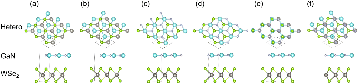 | ||
| Fig. 1 Stereo matching patterns of six canonical parallel configurations of GaN/WSe2 heterostructures. (a) model I, where the N atoms in interface are on the Se atoms straightly; (b) model II, where the Ga atoms are located directly above the middle of the W–Se bonds; (c) model III, where the N atoms in the interface are straightly on top the middle of the W–Se bonds; (d) model IV, where the Ga atoms are located directly above the W atoms; (e) model V, where Ga atoms are located directly on the Se atoms; and (f) model VI, where the N atoms are set on the W atoms. | ||
3. Results and discussion
3.1 Interface stability
To inspect the impact of the interfacial interactions between the GaN and WSe2 nanosheets on the structural stability of GaN/WSe2 combinations, the compositional dependence of the total energy is discussed. Six representative parallel alignments of GaN/WSe2 heterostructures are displayed in Fig. 1. To calculate the structural stability of the six stacked models quantitatively, the D3 and TS dispersion corrections were included to calculate the relative total energies of the six patterns (compared with the steadiest model) applying the PBE method, respectively, as shown in Fig. 2. The results show that the different calculation methods have analogous variation tendencies in the related total energies of the six configurations, demonstrating that the computational outcomes are dependable. Also, the figure shows that model V has the lowest relative energy among the models with the DFT-D3 algorithm, while model VI has the lowest relative energy compared with the others with DFT-TS algorithm. Hence, all sequent calculations were built on these two models.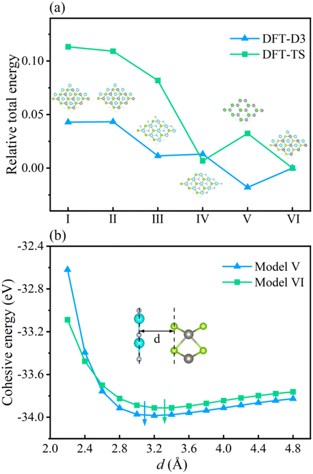 | ||
| Fig. 2 (a) Relative total energies of six models for GaN/WSe2 heterostructures with DFT-TS and DFT-D3 approaches after geometrical optimization, where the illustration exhibits the corresponding side view of the heterostructure. (b) Dependence of the cohesive energies of model V and model VI with interlayer distance d. | ||
To further study the structural stability of the GaN/WSe2 heterostructure, the lattice mismatch ratio and mismatch energy between the two monolayers were calculated. The lattice mismatch ratio is described as Rmis=(a2 − a1)/a1, where a1 and a2 represent the lattice constants of the GaN and WSe2 monolayers, respectively. Table 1 lists the Rmis of the GaN/WSe2 heterostructures calculated by the DFT-D3 and DFT-TS methods, which are 3.00% and 3.92%, respectively, showing a perfect match.31 Moreover, the lattice mismatch energies of the GaN/WSe2 heterostructures were determined using the following equation:
| ΔEmis = [E(GaN)a + E(WSe2)a − E(GaN) − E(WSe2)]/S | (1) |
To elucidate the adsorption interaction between the GaN and WSe2 monolayers, the two above-mentioned methods were chosen to attain the interfacial cohesive energy, Ecoh, at different interlayer distances, d. Ecoh is expressed as follows:
| Ecoh = (EGaN/WSe2 − EGaN − EWSe2)/S | (2) |
Finally, the van der Waals energy was introduced to quantitatively describe the magnitude of the interlayer van der Waals force, which is defined as and its magnitude is determined by the lattice mismatch energy and the interface binding energy. The calculation formula is as follows:
| EvdW = |Ecoh| + |ΔEmis| | (3) |
The calculated results are 2.61 eV and 6.69 eV, which are within the normal vdW binding energy range,37,38 indicating the existence of slight van der Waals forces in the GaN/WSe2 heterostructures.
In the case of the GaN/WSe2 heterostructure, the equilibrium interfacial space between GaN and WSe2 is 3.09 Å with DET-D3 and 3.32 Å with DFT-TS, respectively, which is the canonical distance of vdW force.39 Besides, given that Rmis under DET-D3 is smaller than that with DET-TS, the subsequent calculations are based on model V of the GaN/WSe2 heterostructure with the DET-D3 method. The results of model VI of the GaN/WSe2 heterostructure with the DET-TS method are demonstrated in the ESI.†
3.2 Electronic property
The band arrangements of the GaN monolayer, WSe2 monolayer and GaN/WSe2 composites were investigated using the PBE functional module. The Fermi level of the three systems was set as the level zero energy, and the high symmetry sites G (0,0,0), M (0,0.5,0) and K (−0.333,0.667,0) in the Brillouin zone were used as observation routes to study the band alignment of the system with the range limited from −4 eV to 5 eV. Fig. 3(a) shows that monolayer GaN is a semiconductor with an indirect BG of 2.13 eV, where the valence band maximum (VBM) is settled at the K point, while the conduction band minimum (CBM) is settled at the G point. This is theoretically in accordance with the established research.40 The VBM and CBM of the single-layer WSe2 were both set near the K point, which denotes that WSe2 is a semiconductor with a direct BG of 1.65 eV. The calculated results of WSe2 are similar to that reported by R. S. Meng,41 as demonstrated in Fig. 3(b).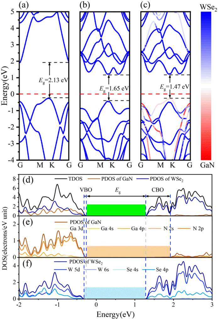 | ||
| Fig. 3 Energy band diagrams of (a) monolayer GaN, (b) WSe2 nanosheet, and (c) model V of GaN/WSe2 heterostructure. (d) Calculated TDOS of GaN/WSe2 heterostructure and PDOS of GaN and WSe2 employing the PBE algorithm. (e) PDOS of Ga and N atoms in GaN. (f) PDOS of W and Se atoms in WSe2. | ||
Fig. 3(c) presents the band diagram of the GaN/WSe2 heterostructure. Both the VBM and CBM are located at the high symmetry point K, and thus it is a direct semiconductor with a BG of 1.47 eV. Compared with the indirect BG semiconductor, the direct bandgap semiconductor has a higher absorption coefficient for photo-generated electron–hole pairs and higher light utilization rate, and thus it is more suitable for photocatalysis.42 The forbidden bandwidth of the GaN/WSe2 heterostructure is 1.47 eV, which is slightly lower than that of the GaN and WSe2 monolayers, and its energy levels are denser. This is conducive to the migration of electrons, thereby improving the photocatalytic activity. Also, the BG of the GaN/WSe2 heterostructure is larger than that required for photocatalytic water splitting, which is 1.23 eV. In addition, comparing the three images in Fig. 3(a–c), it can be found that the energy band structure of the GaN/WSe2 heterostructure is similar to the energy band alignments of the two monolayers, and almost retains that of GaN and WSe2 to a large extent. Therefore, it can be speculated that the binding force between the heterostructure layers is weak van der Waals force, and the interaction force when the two monolayers are combined is small, which also corresponds with the above-mentioned result.
The density of states (DOS) usually reflects the distribution of electrons in each system. To further elucidate the electronic structure of the GaN/WSe2 heterostructure, we also calculated the density of states of the GaN/WSe2 heterostructure, GaN monolayer and WSe2 monolayer. The density curve range was −2 eV to 3 eV for analysis, as illustrated in Fig. 3(e and f). The VBM of monolayer GaN consists mainly of Ga-4p and N-2p states, whereas the CBM consists of N-2p states, are displayed in Fig. 3(e). The VBM and CBM of monolayer WSe2 consist primarily of W-5d and Se-4p states, as presented in Fig. 3(f). Apparently, the VBM is derived from GaN (orange shaded region in Fig. 3(e)), while the CBM of the GaN/WSe2 heterostructure originates from WSe2 (blue shaded region in Fig. 3(f)). The overlap may be caused by orbital hybridization, and the occurrence of orbital overlap will result in a reduction in the BG, which is more advantageous to improve the catalytic performance of the photocatalytic material.43 It is well-known that the valence band offset (VBO) and the conduction band offset (CBO) are at the related sites of the VBM and the CBM of two sides of the interfacial space, respectively, which can considerably modify the charge transfer capacity of the heterostructures under illumination.44 In addition, VBO, CBO, and BG can be defined as ΔEV = EGaN VBM − EWSe2 V, ΔEC = EGaN CBM − EWSe2 CBM, and Eg = EWSe2 CBM − EGaN VBM, respectively. Under the equiponderant interfacial condition, the correlation of VBO, CBO, the BG values is VBO (0.12 eV) < CBO (0.65 eV) < BG (1.47 eV). Accordingly, it can be reliably inferred that the GaN/WSe2 heterostructure shows a type-II or Z-scheme band structure, which is consistent with the conclusion of band alignment, leading to the spatial segregation of the photogenerated carrier pairs.45
The charge transfer phenomenon at the heterostructure interface can be illuminated by calculating the interfacial work function of the GaN monolayer, WSe2 monolayer and GaN/WSe2 heterostructures.46 The calculation formula is as follows:
| W = Evac − EF | (4) |
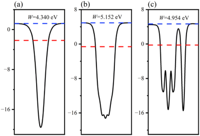 | ||
| Fig. 4 Calculated surface work functions of: (a) GaN monolayer; (b) WSe2 monolayer; and (c) GaN/WSe2 heterostructure. | ||
The position of the band edge of a semiconductor is very important for evaluating its redox ability and photocatalytic performance. It is apparent that with the emergence of heterostructures, the EF of two pristine materials will achieve equilibrium. Consequently, the isolated GaN intimately contacts with WSe2, which will provoke a negative shift of 0.614 V in EF for GaN and induce a positive shift of 0.171 V for the WSe2 nano-slab. Due to the migration of electrons from monolayer GaN to WSe2 with abandoned holes in the GaN nanolayer, the edge potentials in the CB and VB of GaN are −0.73 V and 1.40 V at the GaN/WSe2 heterostructure after equalizing, singly. Meanwhile, that of the WSe2 slab is 0.02 V and 1.67 V, respectively. It can be deduced that the VB edge potential of WSe2 is 0.27 V lower than that of monolayer GaN; meantime, the CB edge of GaN is 0.75 V larger than that of the WSe2 slab. As shown in Fig. 5, the photogenerated carriers obey two different routes, as follows: (1) electron transformation: on the one hand, the photogenerated electrons transfer from the VB to the CB under illumination. On the other hand, the built-in electric field of the interface prevents electrons from migrating from the isolated GaN to WSe2. Meanwhile, the occurrence of CBO impedes electrons implanting in the CB of the monolayer WSe2, and the photo-induced holes in the VB of the single WSe2 hinder their transitions to the VB of the GaN nanosheet. (2) Recombination of charges: in the CB of isolated WSe2, the photogenerated electrons will rapidly recombine with the photogenerated holes in the VB of the isolated GaN, by virtue of the close range of charge conveyance between the WSe2 and GaN layer. Accordingly, photogenerated carriers can excellently detach after the construction of the heterostructure. Finally, it was determined that the GaN/WSe2 heterostructure is a representative direct Z-scheme semiconductor, which is consistent with the consequences of band alignment and DOS. The type of band arrangement can make electron–hole pairs separate effectively and diminish the recombination of carriers, increase the lifetime of minority carriers, and simultaneously retain the redox ability of the internal carriers, which is further enhanced compared to the traditional type-II heterostructure photocatalytic properties.
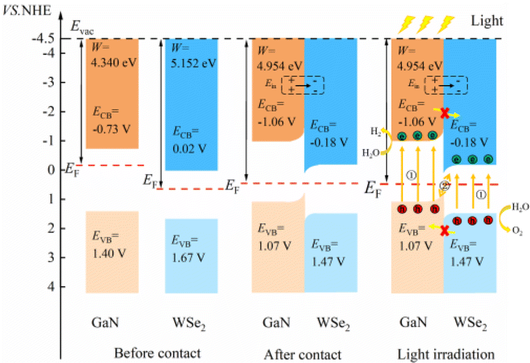 | ||
| Fig. 5 Electronic energy band alignments for isolated GaN and WSe2 before contact, after contact, and under illumination, displaying the segregation and transformation mechanisms of photoinduced charges. | ||
The two important potentials for water splitting are the O2/H2O electrode potential of 1.23 V, which can generate oxygen, and the standard hydrogen electrode H+/H2O potential of 0 V. Given that the GaN/WSe2 heterostructure is a Z-type heterostructure, the potential at the CB position of the heterostructure is −1.06 eV and the VB position is 1.47 eV. Comparing the water splitting potential, it can be known that the energy at the CBM in the GaN/WSe2 heterostructure is more negative than that of the standard hydrogen electrode (H+/H2O), and the VBM is more positive than that of the O2/H2O electrode. The BG of the GaN/WSe2 heterostructure is larger than the potential required for water splitting, and thus it can be deduced that the GaN/WSe2 heterostructure can be applied for either the hydrogen evolution reaction (HER) or oxygen evolution reaction (OER), making it a good photocatalytic heterostructure.
The formation of a heterostructure will induce interactions between the interfaces, leading to the transfer and redistribution of charges at the interface. This can be studied by calculating the differential charge density of the heterostructure. The plane differential density is defined as Δρ, which can be calculated using the following formula:
| Δρ = ρGaN/WSe2 − ρGaN−ρWSe2 | (5) |
For the plane charge differential density curve in Fig. 5, the blue area represents the depletion of charges and the yellow area represents the charge accumulation. Electrons accumulate in the WSe2 slab and are consumed in the GaN slab, elucidating that electrons migrate from the GaN to WSe2 nanosheet. To quantitatively articulate the charge density, the Bader charge analysis under equilibrium was executed. The negative charges of 0.016 e per atom shift from the GaN nanosheet to the WSe2 after they contact each other. It is generally acknowledged that the variation in the populations is consistent with the conclusions of the charge density difference. Simultaneously, in Fig. 5, it indicates that for the benefit of implementing stability, segments of electrons in GaN relocate to WSe2 in the interface, which causes a positive charge region in the surface of GaN and negative charge in that of WSe2. It can be confirmed that the GaN/WSe2 heterostructures can take advantage of the built-in electric field pointing from GaN to WSe2 to efficiently separate the photogenerated electrons and holes (Fig. 6).
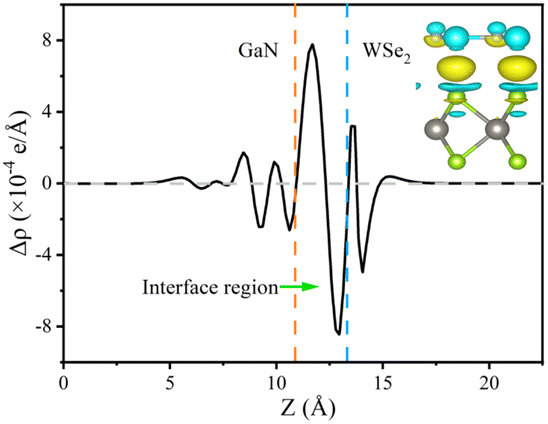 | ||
| Fig. 6 Plane-averaged and 3D charge density difference of GaN/WSe2 heterostructures calculated using the PBE method. The inset shows a side view of the charge density difference of the GaN/WSe2 heterostructure with the isosurface value of 0.0005 e Bohr−3. | ||
3.3 Carrier mobility
Generally, the carrier mobility originates from the deformation potential, which is a pivotal factor to estimate photocatalytic properties and should be calculated systematically.47 The methods for the calculation of the carrier mobility are elaborated in the ESI.† By utilizing compressive and tensile strains, the in-plane C2D and E1i of the isolated GaN, WSe2 and GaN/WSe2 were assessed by fitting the data into parabolic and linear curves, which are exhibited in Fig. 7, S5 and S6 in the ESI,† respectively. Also, Table 2 displays the acquired m*, C2D, E1i and μ2D.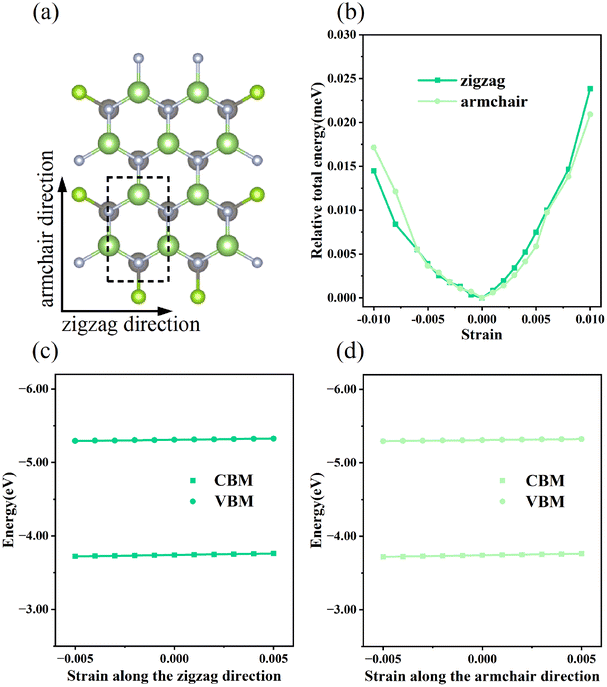 | ||
| Fig. 7 (a) Top vision of orthogonal primitive cell of GaN/WSe2 heterostructure. (b) Variations in relative total energy versus strains of GaN/WSe2. Tendencies of CBM and VBM versus strains for GaN/WSe2, which set Evac as zero-point in the directions of (c) zigzag and (d) armchair. The linear curves offer the deformation potentials of GaN/WSe2 heterostructures. | ||
 and
and  (m0), elastic modulus Czig2D and Car2Dm (Nm−1), deformation potentials Ezig1 and Earm1 (eV), and carrier mobilities μzig2D and μarm2D (cm2 V−1 s−1) of isolated GaN, WSe2 and GaN/WSe2 under the zigzag and armchair traces at 300 K
| Structure | Type |
|
|
Czig2D | Carm2D | Ezig1 | Earm1 | μ2Dzig | μ2Darm |
|---|---|---|---|---|---|---|---|---|---|
| GaN | Electron | 1.01 | 1.83 | 256.16 | 279.78 | −4.30 | −2.46 | 213.93 | 396.91 |
| 171 (ref. 48) | 304 (ref. 49) | ||||||||
| Hole | 1.26 | 1.19 | 256.16 | 279.78 | −0.98 | −1.26 | 3705.20 | 2574.64 | |
| 3185 (ref. 48) | 2396(ref. 49) | ||||||||
| WSe2 | Electron | 1.99 | 2.50 | 203.14 | 177.15 | 2.24 | −3.26 | 193.79 | 63.84 |
| 142 (ref. 50) | |||||||||
| Hole | 1.79 | 2.52 | 203.14 | 177.15 | 1.49 | −2.40 | 511.96 | 122.25 | |
| 583 (ref. 51) | |||||||||
| GaN/WSe2 | Electron | 0.20 | 0.25 | 318.04 | 331.43 | −5.99 | −5.38 | 4149.37 | 4328.33 |
| Hole | 0.54 | 0.61 | 318.04 | 331.43 | −3.22 | −2.91 | 2101.71 | 2395.94 |

The monolayer GaN and WSe2 and GaN/WSe2 heterostructure exhibit different Czig2D and Carm2D in the zigzag and armchair directions, which determines that their physical stress responses are totally anisotropic. In addition, the carrier mobilities of the WSe2 monolayer is lower than that of nanosheet GaN because of its smaller elastic modulus and higher deformation potential. These conclusions are in accordance with previous theoretical and experimental results.48–51 Alternatively, the limitations of the deferent rates of photogenerated carriers are mainly owing to the low electron mobilities of the GaN slab and low carrier mobilities of the WSe2 slab, essentially increasing the recombination of photogenerated electron–hole pairs. Monolayer GaN and WSe2 detrimentally obstruct the photocatalytic activities, and thus is significant to fabricate GaN/WSe2 heterostructures. Consequently, the electron and hole mobilities of the GaN/WSe2 heterostructure are 4149.37 cm2 V−1 s−1 and 2101.71 cm2 V−1 s−1 along the zigzag direction, and 4328.33 cm2 V−1 s−1 and 2395.94 cm2 V−1 s−1 along the armchair direction, respectively, indicating that the electrons in the GaN/WSe2 heterostructure, which have a tendency of spreading and moving along both the zigzag and armchair directions, are superior to holes. Additionally, water oxidation reactions take place in the WSe2 nanosheet through photogenerated holes, the water reduction reactions emerge in the GaN monolayer, as can be seen in Fig. 5. In comparison to the single layers, the electron mobilities of the GaN/WSe2 heterostructure in the zigzag pathway achieve a remarkable enhancement, which are 19 times and 21 times that of the isolated GaN and WSe2, respectively. Meanwhile, 11 times and 67 times versus monolayer GaN and WSe2 are achieved along the armchair pathway. Correspondingly, the hole mobilities of the GaN/WSe2 heterostructure in the zigzag direction and armchair direction are improved by 4 times and 19 times compared with that of nano-slab WSe2, respectively. In short, GaN/WSe2 heterostructures with noticeable carrier mobilities exhibit tremendous potential for application in the photocatalytic field.
3.4 Photocatalytic performance
To additionally validate if water splitting reactions will initiate spontaneously, the thermodynamic practicability of applying the GaN/WSe2 heterostructures as photocatalysts was explored. The complete water splitting mechanism of the GaN/WSe2 heterostructure under light irradiation was divided into the HER and oxygen OER. Herein, the Gibbs free energy (ΔG) of the water splitting reaction were obtained from the report by Nørskov et al.52 The method for the calculations of ΔG is elaborated in the ESI.† Acid (pH = 0) and neutral (pH = 7) conditions were both considered. Universally, the HER tends to occur under a suitable potential than the OER, and thus investigating the thermodynamic driving force for the OER is sufficient.When the OER reaction happens, the structures of the most stable OH*, O*, and OOH* intermediates adsorbed at the WSe2 interface during the standard four-electron transport reaction paths and the relative variation in ΔG are elucidated in Fig. 8. The computed ΔG of OH*, O*, and OOH* in the dark (Uh = 0 V) when pH = 0 is 1.74 eV, 2.81 eV and 4.87 eV, respectively. Therefore, the emergence of the OOH* intermediate is the rate-determining process, and thus the OER process can proceed spontaneously when providing a 1.47 eV external potential afforded by photogenerated holes. It is apparent that the computed ΔG is enhanced in the initial and third steps, but decreases in the second and fourth reaction when pH = 0 and Uh = 1.23 V.
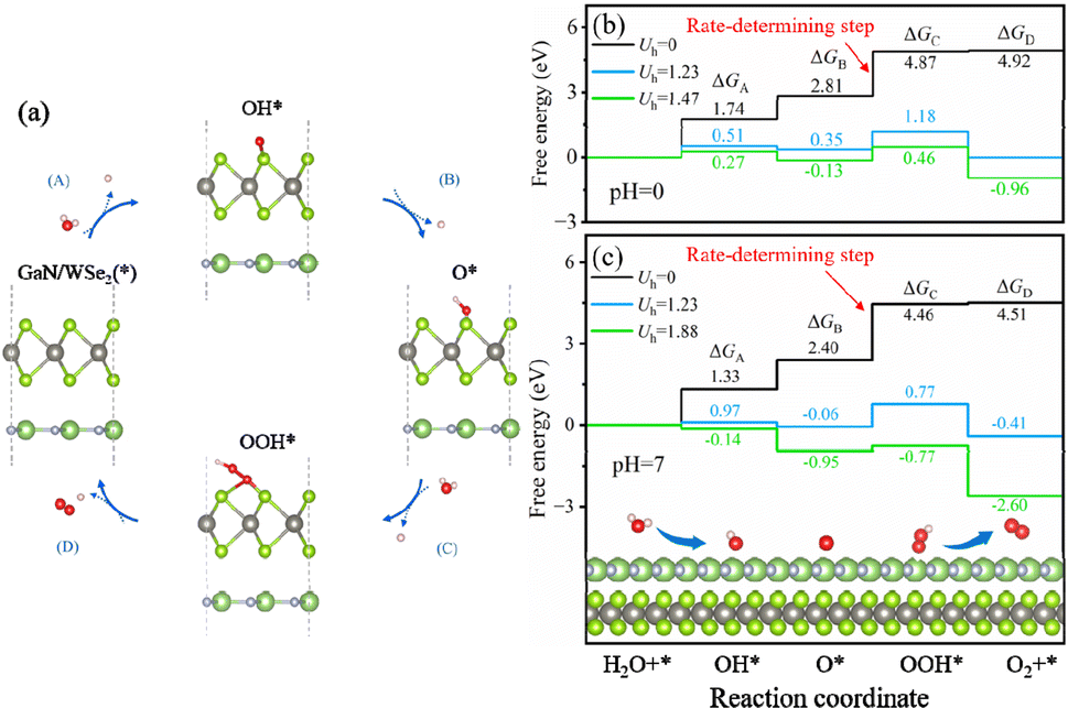 | ||
| Fig. 8 (a) Four-electron route of the OER with the rapid production of OH*, O* and OOH* intermediates on the WSe2 side of the heterostructures. Computational ΔG for the four-electron route of the OER pathway at (b) pH = 0 and (c) pH = 7. | ||
Interestingly, when the external potential realizes 1.67 V with pH = 0, the various trends of ΔG are the same as the conditions at pH = 0 and Uh = 1.23 V. The results indicate that the OER step of water splitting will not spontaneously originate at pH = 0. Until the external potential reaches 1.88 V at pH = 7, the ΔG of the ultimate processes (ΔGA, ΔGB, ΔGC, and ΔGD) shifts to negative values, as exhibited in Fig. 8(c) (presented by the green line), which ascertains that the OER process will spontaneously occur at pH = 7 with light illumination. In conclusion, the GaN/WSe2 heterostructures can initiate water decomposition without a thermodynamic driving force under irradiation in a neutral environment.
4. Conclusions
In summary, we comprehensively investigated the electronic, optical and photocatalytic properties of the GaN/WSe2 heterostructure. Model V manifested a beneficial Z-scheme band arrangement with a built-in electric field pointing from GaN to WSe2, while model VI displayed a detrimental type I band alignment. In the case of model V, the electron mobilities of the GaN/WSe2 heterostructure are significantly enhanced compared to that of monolayer GaN and WSe2, and the hole mobilities enlarge substantially compared to that of isolated WSe2. In addition, the CB edge of GaN and VB edge of the WSe2 monolayer can yield robust reduction and oxidation reaction, respectively. Then, we explored the photocatalytic OER on the heterostructure and found that the reaction spontaneously proceeded in a neutral environment. These findings provide a theoretical basis for the practical application of 2D GaN/WSe2 heterostructures and provide insight for subsequent research on van der Waals heterostructures.Conflicts of interest
The authors declare no competing financial interest.Acknowledgements
This work was supported by East China University of Science and Technology (200237). This work was financed by Science and Technology Commission of Shanghai Municipality, China [Grant No. 17DZ1201405].References
- W. Ager Joel and A. Lapkin Alexei, Science, 2018, 360, 707–708 CrossRef CAS PubMed.
- F. Gutiérrez-Martín, A. B. Calcerrada, A. de Lucas-Consuegra and F. Dorado, Renewable Energy, 2020, 147, 639–649 CrossRef.
- C. J. Quarton, O. Tlili, L. Welder, C. Mansilla, H. Blanco, H. Heinrichs, J. Leaver, N. J. Samsatli, P. Lucchese, M. Robinius and S. Samsatli, Sustainable Energy Fuels, 2020, 4, 80–95 RSC.
- Y. Wu, C. Cao, C. Qiao, Y. Wu, L. Yang and W. Younas, J. Mater. Chem. C, 2019, 7, 10613–10622 RSC.
- H. Zhuang, W. Chen, W. Xu and X. Liu, Int. J. Energy Res., 2020, 44, 3224–3230 CrossRef CAS.
- W. Zhao, Z. Ghorannevis, L. Chu, M. Toh, C. Kloc, P. H. Tan and G. Eda, ACS Nano, 2012, 7, 791–797 CrossRef PubMed.
- G. Hao, R. Zhang and W. Zhang, et al., Acta Phys. Sin., 2022, 71, 01–04 Search PubMed.
- P. Tonndorf, R. Schmidt, P. B Ttger, X. Zhang, J. B. Rner, A. Liebig, M. Albrecht, C. Kloc, O. Gordan and D. Zahn, Opt. Express, 2013, 21, 4908–4916 CrossRef CAS PubMed.
- X. Zhang, Z. Meng, D. Rao, Y. Wang, Q. Shi, Y. Liu, H. Wu, K. Deng, H. Liu and R. Lu, Energy Environ. Sci., 2016, 9, 841 RSC.
- H. Wang, X. Li and J. Yang, ChemPhysChem, 2016, 17, 2100 CrossRef CAS PubMed.
- W. Hu, J. Yang and B. N. L. E. Lawrence, J. Mater. Chem. C, 2017, 5, 12289–12297 RSC.
- W. Xia, L. Dai, P. Yu, X. Tong, W. Song, G. Zhang and Z. Wang, Nanoscale, 2017, 9, 4324–4365 RSC.
- J. LOW, J. YU and M. JARONIEC, et al., Adv. Mater., 2017, 29, 1601694 CrossRef PubMed.
- J. Yu, et al., Phys. Chem. Chem. Phys., 2013, 15, 16883–16890 RSC.
- A. Meng, B. Zhu, B. Zhong, L. Zhang and B. Cheng, Appl. Surf. Sci., 2017, 422, 518–527 CrossRef CAS.
- F. Liu, R. Shi, Z. Wang, Y. Weng, C. M. Che and Y. Chen, Angew. Chem., Int. Ed., 2019, 58, 11791–11795 CrossRef CAS PubMed.
- H. Ahin, S. Cahangirov, M. Topsakal, E. Bekaroglu and S. Ciraci, Phys. Rev. B: Condens. Matter Mater. Phys., 2009, 80, 155453 CrossRef.
- A. R. Fareza, F. A. Nugroho, F. F. Abdi and V. Fauzia, J. Mater. Chem. A, 2022, 10, 24280 RSC.
- W. M. Hoi, B. Oliver and R. J. Kaplar, et al., J. Mater. Res., 2021, 23, 36 Search PubMed.
- P. Gupta, et al., Sci. Rep., 2016, 6, 23708 CrossRef CAS PubMed.
- M. Tangi, P. Mishra, C. Tseng, T. K. Ng, M. N. Hedhili, D. H. Anjum, M. S. Alias, N. Wei, L. Li and B. S. Ooi, ACS Appl. Mater. Interfaces, 2017, 9, 9110–9117 CrossRef CAS PubMed.
- R. Meng, et al., Sci. China Mater., 2016, 59, 1027–1036 CrossRef CAS.
- S. Yin, Q. Luo, W. Dong, G. Guo, X. Sun, Yi Li, Y. Tang, Z. Feng and X. Dai, Phys. E: Low-Dimens. Syst. Nanostructures, 2022, 142, 115258 CrossRef CAS.
- G. Kresse and J. Furthmüller, Phys. Rev. B: Condens. Matter Mater. Phys., 1996, 54, 11169–11186 CrossRef CAS PubMed.
- J. P. Perdew, K. Burke and M. Ernzerhof, Phys. Rev. Lett., 1996, 77, 3865–3868 CrossRef CAS PubMed.
- A. Tkatchenko and M. Scheffler, Phys. Rev. Lett., 2009, 102, 073005 CrossRef PubMed.
- S. Grimme, J. Antony, S. Ehrlich and H. Krieg, J. Chem. Phys., 2010, 132, 154104 CrossRef PubMed.
- Y. Jiang, et al., Comput. Mater. Sci., 2017, 138, 419–425 CrossRef CAS.
- R. Zhang, G. Hao and X. Ye, et al., J. Appl. Phys., 2021, 129, 174302 CrossRef CAS.
- Yi Ding, et al., Phys. B, 2011, 406, 2254–2260 CrossRef CAS.
- J. He, M. Zhang and Q. Xiao, J. Nanjing Univ., 2006, 1, 63–102 Search PubMed.
- K. Si, J. Ma, C. Lu, Y. Zhou, C. He, D. Yang, X. Wang and X. Xu, Appl. Surf. Sci., 2020, 507, 145082 CrossRef CAS.
- R. Zhang, G. Hao, X. Ye, S. Gao and H. Li, Phys. Chem. Chem. Phys., 2020, 22, 23699–23706 RSC.
- K. Si, J. Ma, C. Lu, Y. Zhou, C. He, D. Yang, X. Wang, X. X. Xu, C. Wang, W. Xiong, Y. Liu, D. Yang, X. Zhang and J. Xu, Nanotechnology, 2021, 33, 085705 Search PubMed.
- C. He, F. S. Han, J. H. Zhang and W. X. Zhang, J. Mater. Chem. C, 2020, 8, 6923–6930 RSC.
- R. Zhang, G. Hao, H. Li, X. Ye, S. Gao, X. Yuan and C. Liu, J. Phys. Chem. Solids, 2020, 143, 109466 CrossRef CAS.
- D. K. Gorai and T. K. Kundu, Appl. Surf. Sci., 2022, 590, 153104 CrossRef CAS.
- R. Zhang, G. Hao and X. Ye, et al., Phys. Chem. Chem. Phys., 2020, 22, 23699–23706 RSC.
- W. Zhang, G. Hao and R. Zhang, et al., J. Phys. Chem. Solids, 2021, 157, 110189 CrossRef CAS.
- X. T. Zhu, Y. Xu, Y. Cao, Y. Q. Zhao, W. Sheng, G. Z. Nie and Z. Ao, Appl. Surf. Sci., 2021, 542, 148505 CrossRef CAS.
- R. S. Meng, Sci. China Mater., 2016, 59(12), 1027–1036 CrossRef CAS.
- P. Shan, SIn2Te/TeIn2Se: a type-II heterojunction as a water-splitting photocatalyst with high solar energy harvesting, Xiangtan Univ., 2021 Search PubMed.
- F. Zhou, H. Xiang, J. Liu and B. Liu, Mater. Eng., 2018, 46, 9–19 Search PubMed.
- Z. Chen, X. Ma, J. Hu, F. Wan, P. Xu, G. Wang, M. Wang, S. Deng and C. Huang, New J. Chem., 2021, 45, 16520–16528 RSC.
- R. Zhang, G. Q. Hao, H. B. Li, X. J. Ye, S. Gao, X. Yuan and C. Liu, J. Phys. Chem. Solids, 2020, 143, 109466–109471 CrossRef CAS.
- G. Hao, R. Zhou and W. Lei, et al., Phys. Chem. Solids, 2022, 165, 110684 CrossRef CAS.
- F. Zhuang, H. Guoqiang, R. Zhou, W. Lei, Y. Deng, X. Ye, H. Li and R. Zhang, Mater. Today Commun., 2022, 33, 104295 CrossRef CAS.
- W. J. Yin, X. L. Zeng, B. Wen, Q. X. Ge, Y. Xu, G. Teobaldi and L. M. Liu, Front. Phys., 2021, 16, 11467 Search PubMed.
- K. Ren, Y. Liu, J. Yu and W. C. Tang, Chem. Phys., 2020, 528, 110539 CrossRef CAS.
- W. Liu, J. Kang, D. Sarkar, Y. Khatami, D. Jena and K. Banerjee, Nano Lett., 2013, 13, 1983–1990 CrossRef CAS PubMed.
- R. Zhang, F. Zhuang and R. Zhou, et al., J. Phys. Chem. Solids, 2022, 171, 111014 CrossRef CAS.
- J. K. Nørskov, J. Rossmeisl, A. Logadottir, L. Lindqvist, J. R. Kitchin, T. Bligaard and H. Jónsson, J. Phys. Chem. B, 2004, 108, 17886–17892 CrossRef.
Footnotes |
| † Electronic supplementary information (ESI) available. See DOI: https://doi.org/10.1039/d3ra00928a |
| ‡ Co-first authors: these authors contributed equally. |
| This journal is © The Royal Society of Chemistry 2023 |