
 Open Access Article
 This Open Access Article is licensed under a Creative Commons Attribution-Non Commercial 3.0 Unported Licence
Electrodeposition and characterization of Sn on Re filaments for laser resonance ionization mass spectrometry
Jiangfan Wang *,
Jinlong Fan,
Wenliang Wang,
Xiangbo Zhang,
Lei Feng,
Xiufang Zhai,
Xiaopan Shen and
Zhiming Li
*,
Jinlong Fan,
Wenliang Wang,
Xiangbo Zhang,
Lei Feng,
Xiufang Zhai,
Xiaopan Shen and
Zhiming Li
Northwest Institute of Nuclear Technology, Xi'an, Shaanxi 710024, PR China. E-mail: wangjiangfan@163.com
First published on 3rd April 2023
Abstract
The isotopic analysis of Sn is crucial for geochemical research and surveillance of nuclear contamination. However, commonly used methods face the challenge of isobaric interference. Laser resonance ionization mass spectrometry (LRIMS) is a promising technology for effectively eliminating the isobaric interference effect as it combines the advantages of both resonance ionization and mass spectrometry technologies. In this study, an atomic source of 1 μg Sn was prepared by electrodeposition on a Re filament in a 1–5 × 0.7 mm spot for LRIMS measurement. The effects of voltage, duration, length of the active area, and Pb content on the deposition yield were studied, and the morphology, composition, and valence of the Sn deposits were examined. A maximum yield of over 90% in a 3 × 0.7 mm spot was achieved through the surface modification of Re filaments and optimisation of the electrodeposition parameters. As the Sn0 atomic state was predominant in the deposit, the average detection efficiency of the LRIMS device using the as-deposited Sn samples was approximately 3.63 × 10⁻⁴, which was almost an order of magnitude higher than that of the sample dropped with graphene oxide solution (4.39 × 10⁻⁵).
1. Introduction
Owing to its special geochemical behaviour in silicate earth, the abundance of Sn is a result of both the segregation of metals during core formation and volatility-related depletion in the precursor materials from which earth is formed.1 The isotopic analysis of Sn provides “fingerprints” of bronze artifacts that can be matched to their parental ore sources.2 In addition, 23 radioactive isotopes are produced during fission production, among which 126Sn and 121mSn are considered important nuclides for monitoring nuclear contamination.3,4 Therefore, the isotopic analysis of Sn is particularly promising and has already found many applications in diverse fields, such as geological studies and the characterisation of nuclear waste.The conventional methods of isotopic analysis are inductively coupled plasma mass spectrometry (ICP-MS),5 thermal ionization mass spectrometry (TIMS),6 and accelerator mass spectrometry (AMS).7 Nevertheless, isobaric interference is inevitable. Therefore, a complex sample preparation chemistry procedure is commonly adopted to separate isobars, which may result in sample waste and introduce interferences. Laser resonance ionization mass spectrometry (LRIMS) is a promising technology which combined with the advantages of both resonance ionization and mass spectrometry technology.8–10 The combination of two powerful techniques ensures high elemental and isotopic selectivity and thus can effectively overcome the problem of isobaric interference faced by commercial mass spectrometry.
As the preparation of an atomic source is crucial for obtaining ideal detection results for LRIMS, considerable efforts have been made to study the theoretical and experimental conditions to optimise the parameters affecting the detection efficiency and reproducibility.11–15 For decades, researchers from Mainz University in Germany, and the Paul Scherrer Institute in Switzerland, have developed techniques for the preparation and characterization of a sandwich source for actinide measurement.13,14 The actinide oxide is usually electrodeposited on a Re/Ta filament within a 2–3 mm spot and subsequently covered with a thin reductive metal coating. During the heating process of such a sandwich filament, actinide oxide is reduced to the metallic state while diffusing through the coated metal and an atomic beam evaporates from the surface. In contrast to the actinide elements, the concentration of Sn that mainly originates from the background is near the ppm level and Sn can be directly reduced to the atomic state because of its positive electrode potential. To the best of our knowledge, no other atomic sources have been prepared by electrodeposition for LRIMS determination, except for actinide elements and Tc.16 Since electrodeposition is often used for the preparation of thin, uniform radioactive layers applied as targets or as counting samples,17 it is worth preparing an electrodeposited Sn atomic source for LRIMS as it may enhance the detection efficiency.
Currently, Sn sources are usually prepared by directly dropping sample solutions or mixing solutions containing the samples and graphene oxide.4,18 Sn species exist as complex compounds, which is disadvantageous for obtaining efficient atomic beam sources.19 In this study, an atomic source of 1 μg Sn was prepared by electrodeposition on a Re filament, and the optimized parameters were explored to achieve an ideal yield. The detection efficiencies of the as-deposited Sn samples and traditional sources by dropping were then determined using the LRIMS device for comparison.
2. Experimental
2.1 Preparation of Sn on Re filaments
The schematic diagram of the apparatus used for electrodeposition is shown in Fig. 1. Some modifications of a conventional electrodeposition cell for alpha spectrometry were made because of the small spot diameter. The apparatus was placed in a water bath to maintain a constant temperature. Before electrolysis, Re filaments (45 μm thick, 0.7 mm wide) were treated with 6 M HCl at 100 °C for 10 min. Subsequently, they were ultrasonically cleaned with deionized water before electrodeposition. For comparison, some Re filaments were modified in a special etchant solution for 10 min and ultrasonically cleaned with deionized water before electrodeposition. The composition of the etchant solution was 10 g K3Fe(CN)6 + 10 g KOH + 100 mL distilled water. The as-treated Re filament was then fixed on an adhesive tape-coated stainless steel block using a PE cap. A quartz funnel contained the electrolyte and confined the area to be plated to a diameter of 1–5 mm. A platinum wire and a Re filament served as the anode and cathode, respectively, which were connected to an external power supply that delivered constant voltage. The electrolyte solution was composed of 1 μg Sn (SnCl2) and 0–10 μg Pb (Pb(NO3)2) in 2 M HCl. The primary electrodeposition parameters are listed in Table 1. The details for preparing the Sn sources by directly dropping a mixing solution containing Sn and graphene oxide have been reported in our previous work.4,18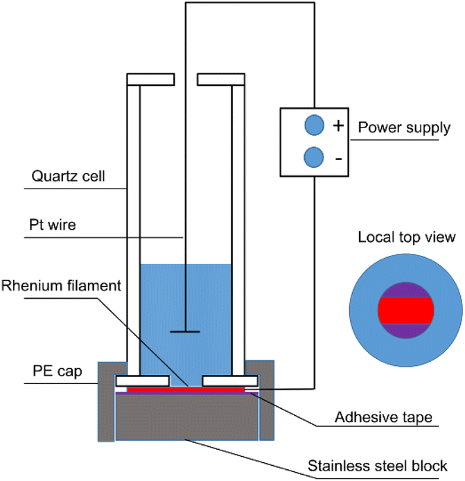 | ||
| Fig. 1 Schematic diagram of the electrodeposition apparatus. | ||
| Voltage/V | Deposition time/h | Pb content/μg | Length of active area/mm | Distance between electrodes/mm | Bath temperature/°C |
|---|---|---|---|---|---|
| 1.8–2.2 | 0–4 | 0–10 | 1–5 | 5 | 60 |
2.2 Characterization
The surface morphology of the as-deposited Sn samples was observed using a scanning electron microscope (SEM, TESCAN MIRA4 and Quanta FEG 250). The chemical composition was examined using energy-dispersive X-ray spectroscopy (EDS) attached to the SEM system. To characterize the wettability of the Re surfaces before and after the modification process, the contact angle of the water droplets on powder metallurgy (PM) Re plate was measured using a commercial water contact angle meter at room temperature. At least five datasets from different locations were averaged. Chemical surface characterization was performed by X-ray photoelectron spectroscopy (XPS), and Al-Kα radiation was used. The X-ray source was operated at an anode voltage of 12 kV and a current of 6 mA. The experimental uncertainty of the binding energies was 0.1 eV, and the spectra were calibrated by a C 1s peak at 284.8 eV. To further investigate the Sn species, high-resolution XPS spectra of the Sn 3d region at different sputtering depths with Ar+ ions were obtained. To determine the electrodeposition yields under different process parameters, a Sn electrolyte containing a radioactive 113Sn (113Sn, t1/2 = 115.1 d, Eγ = 391.7 keV) tracer was measured before and after the electrodeposition process via γ-ray spectroscopy. To produce the electrolyte containing the 113Sn radioactive tracer, condensate 112Sn metallic powder was irradiated with thermal neutrons in the Xi'an Pulsed Reactor and subsequently dissolved in 2 M HCl. The detection efficiency of the as-deposited sample and the sample dropped with graphene oxide solution were determined for comparison using the LRIMS device developed in our laboratory. The structure of the LRIMS device is shown in Fig. 2, mainly including: laser system, atomization source, magnetic mass analyzer, data acquisition and processing system. An efficient three-color three-photo resonance ionization scheme of Sn was confirmed. The laser wavelengths of each excitation/ionization step were optimized as λ1 = 286.4 nm, λ2 = 811.6 nm, λ3 = 823.7 nm and other detailed test parameters were reported in ref. 4. The LRIMS detection efficiency is defined as the ratio of the number of ions counted by the detector to the number of atoms originally present on the filament. | ||
| Fig. 2 Schematic diagram of the LRIMS setup.4 | ||
1. Nd: YAG laser; 2. dye laser; 3. BBO crystal; 4. laser monitor and control; 5. laser wavelength meter; 6. laser power meter; 7. fiber combiner; 8. output lens; 9. atomizer; 10. thermo shield; 11. ion lens; 12. mass analyser; 13. power supply and vacuum; 14. ion collector; 15. Faraday cups; 16. secondary electron multiplier; 17. digital recorder.
3. Results and discussion
3.1 Preparation of Sn on Re filaments
The surface morphology of the deposits obtained during the first exploration is shown in Fig. 3(a). Scattered spheres were distributed along the flat surface of the Re filament. Interestingly, many circular shapes (marked with red circles) are regularly aggregated by spheres. The distribution of the spherical grains may be attributed to the bubble effect. For an aqueous deposition process for Sn2+ with a much lower content compared to H+, a hydrogen evolution reaction is inevitable at the cathode. The formation process of H2 bubbles is illustrated in Fig. 3(c), and it comprises three steps. First, the H+ ions receive the majority of the electrons from the cathode and are reduced to adsorptive H atoms, among which two H atoms combine to form an H2 molecule. Subsequently, H2 molecules are incorporated to form small hydrogen bubbles. Finally, small hydrogen bubbles evolve into larger bubbles to minimize the surface energy. Further, the bubbles prefer to attach to the solid surface and continue to grow until they burst or leave the solid surface under the influence of buoyancy. The bubbles evolve and disappear sequentially during the electrodeposition. | ||
| Fig. 3 Surface micromorphology of Sn deposit on (a) original Re filament and (b) surface modified Re filament; (c) schematic diagram of gas evolution process on limited cathode surface; paving status and contact angles of water on the (d) original and (e) modified PM Re plates. | ||
In the micro-electrodeposition process performed herein, the bubble size is comparable to the active area (3 mm × 0.7 mm) and the bubbles are sufficiently large to cover the entire cathode surface. During the electroplating process performed on the original Re filament, bubbles developed and disappeared repeatedly and sequentially approximately at the specific site of the Re filament. Accordingly, the current fluctuated significantly under a constant voltage. The fluctuation period of the current was consistent with bubble generation and disappearance (see Fig. 4(a)). If left undisturbed, these bubbles can act as insulators and slow down or even stop the electroplating process. To sustain a continuous electroplating process, it is necessary to manually dislodge the gas bubbles once they completely cover the cathode surface. Therefore, the electrodeposition process is not reliable for achieving an ideal yield under strong and repeated bubble interference.
 | ||
| Fig. 4 Current versus time curves recorded for the electrodeposition process performed on the (a) original Re filament and (b) surface modified Re filament under a constant voltage of 2.0 V. | ||
In general, the wettability of a substrate is closely related to the quality of the electrodeposited coating. Poor wetting of the substrate usually leads to defects such as pinholes and delamination of thick coatings.20 From this perspective, the adverse effects of bubbles can be avoided by improving the hydrophilicity of the cathode surface so that the bubbles can spontaneously leave the cathode surface before they are sufficiently large to cover the entire area. The hydrophilicity of a metal surface can be enhanced by endowing special microstructures to improve the surface energy via corrosion treatment or electrochemical dissolution.21,22 Therefore, we modified the Re filament by corrosion treatment in a freshly prepared etchant solution before electrodeposition. The paving status and contact angle of the water on the original and modified PM Re plates at room temperature are shown in Fig. 3(d) and (e). The average contact angles of water on the original and modified PM Re plates were 77.5° and 37.4°, respectively, indicating that wettability was remarkably improved by modifying the Re plate surface. As expected, the current maintained steadily during the electroplating process under constant voltage (see Fig. 4(b)). Fig. 3(b) shows the surface morphology of the Sn deposit on the modified Re filament. The circular shapes aggregated by the spheres, as shown in Fig. 3(a), disappeared; instead, the filament surface was full of micro-grooves attached to many spheres, indicating a much higher electrodeposition yield. The electrodeposition yields determined by the radioactive 113Sn tracer before and after the modification of Re filaments were 12% and 36%, respectively. This indicates that the existence of micro-grooves plays a significant role in improving the surface roughness (wettability), thus providing more simultaneous active sites (yield) in a limited area.
To obtain an ideal yield, the effects of the main parameters on the deposition yield were systematically studied, and the results are presented in Fig. 5. The formation of alloys usually facilitates the reduction of metal ions under a certain electrical field, and the reduction potential of Pb is close to that of Sn. Therefore, it would be beneficial to add some Pb to the electrolyte to promote Sn reduction, while the LRIMS measurement results will not be affected by Pb in the deposit. The effect of the Pb content on the deposition yield is shown in Fig. 5(a). With an increase in the Pb content in the electrolyte from 1 μg to 5 μg, the deposition rate in a 3 × 0.7 mm spot increases from 37% to 90%. However, it decreases to 82% as the Pb content continues to increase to 10 μg, which may be attributed to the low capacity of the small active area. Thus, the optimal Pb content is 5 μg. Under ideal circumstances, the deposits on the Re filament should be within the action region of the laser beam during the LRIMS measurement. To obtain maximum detection efficiency, the length of the active area to be electrodeposited should be less than 2 mm (diameter of the laser beam). The yields of Sn deposits prepared on Re filaments with different active area lengths are shown in Fig. 5(b). The deposition yields are 17.5%, 92%, and 94%, with the lengths ranging from 1 mm to 5 mm, indicating that the length of the active area on the Re filament should be longer than 3 mm to achieve a deposition yield over 90%. As the active area decreases, hydrogen evolution reaction becomes more concentrated. Consequently, the effect of hydrogen embrittlement cannot be ignored; the Re filament of 1 mm in length of the active area was fractured at the boundary after electrodeposition. Considering both the deposition yield and detection efficiency, the optimal length of the Re filament to be electrodeposited was set to 3 mm. As shown in Fig. 5(c), when the applied voltage is lower than 2.0 V, the deposition yield increases gradually with increasing voltage and reaches a maximum in the range of 2.0–2.1 V. Contrarily, as the applied voltage continues to increase, the deposition yield declines markedly. The variation in the deposition yield with the applied voltage can be attributed to the change in the reduction reaction at different potentials. The electrochemical reduction of Sn2+ is inefficient at a voltage below 2.0 V. In contrast, when the applied voltage exceeds 2.1 V, a competitive reduction between H+ and Sn2+ occurs on the cathode surface. For an acidic electrolyte (2 M HCl), the hydrogen evolution reaction was inevitable, and the bubbles attached to the cathode surface hindered the normal reduction of Sn2+. Finally, the yield was further studied for different electroplating times at a constant voltage of 2.0 V. The electrodeposition time was found to significantly affect the yield for micro-electrodeposition, which is consistent with the conclusions.23,24 As shown in Fig. 5(d), when the deposition time is less than 2 h, the yield increases with the duration. With the extension of time, the rising rate slows down and reaches a plateau in 4 h. This duration is much longer than that of traditional electrodeposition for alpha spectrometry to obtain a satisfactory yield. As more time is required for the trace element to sufficiently diffuse to the small surface of the cathode, the diffusion process is also disturbed by the bubble evolution process.
 | ||
| Fig. 5 The effect of (a) Pb content, (b) length of active area, (c) voltage and (d) time on the deposition yields of Sn prepared on Re filaments. | ||
3.2 Characterization and measurement of Sn on Re filaments
Fig. 6 shows the surface micromorphology of Sn deposits on the Re filament for the optimised parameters. The Sn deposits are relatively uniform under lower magnification (Fig. 6(a) and (b)), whereas, at higher magnification, the deposits are composed of inhomogeneously distributed nanoscale dendrites. The majority of deposits preferentially congregate near the grain boundaries and then develop into typical dendrites (Fig. 6(d)), whereas fine and scattered dendrites are dispersed within the grains of the Re filament (Fig. 6(c)). The results suggest that the defects on the modified Re surface subsequently act as centres for preferential growth. The chemical composition was then examined using EDS attached to the SEM system (Fig. 6(e)). The results indicate that the deposit was a mixture of different species containing O, Pb, Cl, Sn, and Pt. The presence of Pt originating from the dissolution of the anode has been reported in many studies.19,25 Moreover, dissolved Pt may act as a carrier for trace elements during electrodeposition. Pb originates from the co-deposition with Sn owing to the contiguous reduction potential and Re from the filament substrate. However, the existence of O and Cl suggests that complex side reactions occur during electrodeposition. | ||
| Fig. 6 (a–d) Surface micromorphology and (e) EDS analysis of Sn deposits on the Re filament. | ||
In contrast to EDS, XPS has a significantly high surface sensitivity. By obtaining high-resolution XPS spectra, we further examined the oxidation state of the deposits. According to the BE position, the Sn 3d peaks at lower BE correspond to the Sn0 state, and the peaks at higher BE correspond to Sn2+ oxidation states (see Fig. 5(d), 7(a)).26 The XPS results indicate that Sn was present as a mixture of Sn0 and Sn2+ oxidation states, and the Sn2+ oxidation state was predominant on the deposit surface, which contradicts our expectations (see Fig. 7(a)). To further investigate the nature of the Sn species, high-resolution XPS spectra of the Sn 3d region at different sputtering depths with Ar+ ions were obtained. As expected, the Sn0 component increased from 22.8% to 70.9%, with the etching depth increasing from 0 nm to 30 nm. Considering that the XPS beam spot (400 μm) was much larger than the grain size, it was difficult to obtain complete depth profile information of specific grains undisturbed from the adjacent grains. Therefore, increasing the etching depth further to achieve a complete Sn0 component is meaningless. Considering the entire range, the Sn0 component still accounted for the majority of the Sn species in the deposits. Therefore, we may speculate that the Sn2+ content was too low and precipitated together with other impurities at a certain stage during the electrodeposition process, which is consistent with the appearance of O and Cl elements in the EDS results.
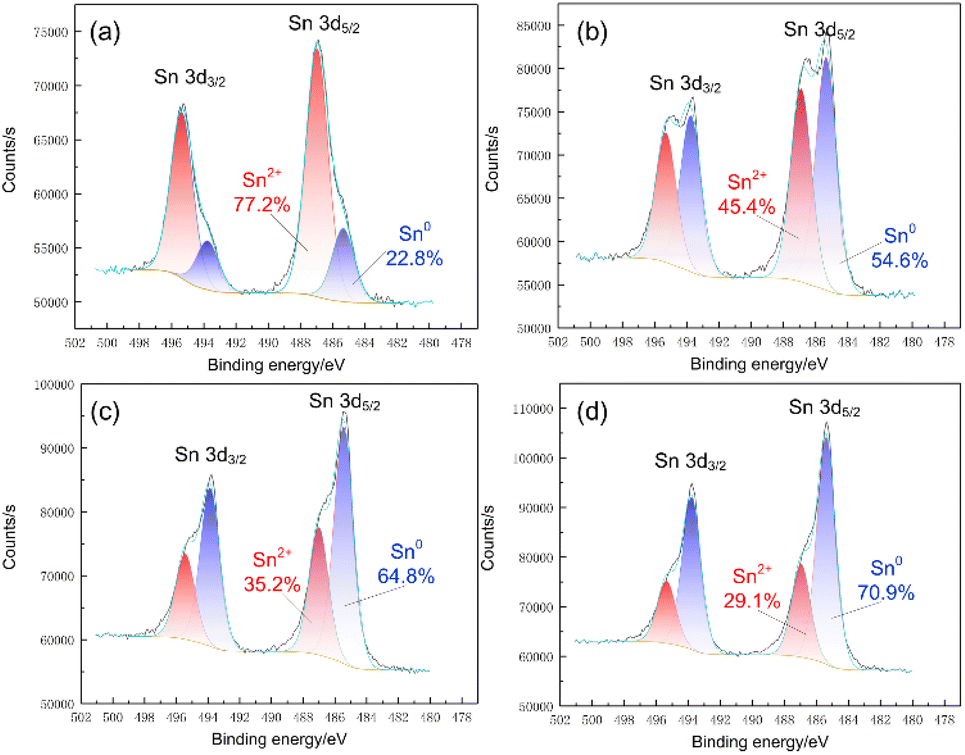 | ||
| Fig. 7 High-resolution XPS spectra of Sn 3d region and single-peak fit to the data for different etching depth: (a) 0 nm; (b) 10 nm; (c) 20 nm; (d) 30 nm. | ||
For the convenience of measurement, an electrolyte containing 1 μg of natural Sn was used to prepare the source for the LRIMS test at the optimized parameters. The sample was then assembled in an apparatus dedicated to an LRIMS device. The total detection efficiency of the LRIMS device was determined using the as-deposited sample, dropping the sample with graphene oxide solution for comparison. During the test, a current was applied to the filament and the photo-induced ion signal of 120Sn was monitored by the Faraday cup. The filament was heated to a temperature where a stable count rate was achieved. Whenever the count rate decreased, the current was increased further until the desired count rate was reached. This was repeated until the signal faded completely. The temperature of the filament was monitored by an infrared temperature detector and the temperature range was from the room temperature to ∼1200 °C. The test time for each sample was about 30 minutes. The total number of 120Sn ions counted by the detector was obtained by integrating the curve over the detection time. The LRIMS detection efficiency is defined as the ratio of the number of ions counted by the detector to the number of atoms originally present on the filament (the total amount of Sn on the filament was treated as 1 μg and the abundance of 120Sn as 32.85%). The results of multiple measurements showed that the average detection efficiency of the as-deposited Sn sample was approximately an order of magnitude higher than that of the samples dropped with graphene oxide solution. The distinct difference in Table 2 can be attributed to the different existing species of Sn in the filaments prepared using different methods. Regarding the deposited Sn source, the Sn0 component accounted for the majority of the Sn species in the deposits. As for the Sn source prepared by dropping the sample mixed with graphene oxide, the Sn species remained complex compounds and had to be reduced by graphene oxide before resonance excitation and ionization, which is disadvantageous for obtaining an efficient atomic beam source. Therefore, electrodeposition has a congenital advantage over other methods for the preparation of Sn sources for higher detection efficiency.
| Sample no. | Drop samples mixed with graphene oxide | As-deposited samples |
|---|---|---|
| 1# | 1.29 × 10⁻⁵ | 7.4 × 10⁻⁴ |
| 2# | 6.14 × 10⁻⁵ | 4.7 × 10⁻⁴ |
| 3# | 4.39 × 10⁻⁵ | 3.0 × 10⁻⁴ |
| 4# | 6.46 × 10⁻⁵ | 2.8 × 10⁻⁴ |
| 5# | 4.20 × 10⁻⁵ | 2.3 × 10⁻⁴ |
| 6# | 1.97 × 10⁻⁵ | 2.8 × 10⁻⁴ |
| 7# | 2.07 × 10⁻⁵ | 2.4 × 10⁻⁴ |
| 8# | 2.30 × 10⁻⁵ | — |
| 9# | 1.07 × 10⁻⁴ | — |
| Average values | 4.39 × 10⁻⁵ | 3.63 × 10⁻⁴ |
| RSD/% | 64.60 | 50.80 |
4. Conclusions
An atomic source of 1 μg Sn was prepared by electrodeposition on a Re filament for detection efficiency enhancement of LRIMS, and the optimized parameters were explored to achieve the optimal yield.The results show that surface modification of the Re filament was crucial for maintaining a reliable and consistent deposition process by increasing the wettability and offering more active sites for subsequent preferential precipitation. The average contact angles of water on the original and modified Re surface were 77.5° and 37.4°, respectively. The electrodeposition yield within an active area of 3 mm × 0.7 mm exceeded 90% for the optimized parameters. The deposits were typical nanoscale dendrites and presented a mixture of different species containing O, Pb, Cl, Sn, and Pt. Sn was present as a mixture of Sn0 and Sn2+ oxidation states; the latter was predominant on the deposit surface, whereas the Sn0 component increased with the etching depth and progressively became the primary species in the deposits.
The LRIMS test results showed that the average detection efficiency of the as-deposited Sn samples (3.63 × 10⁻⁴) was approximately an order of magnitude higher than that of the samples dropped with graphene oxide solution (4.39 × 10⁻⁵). The striking results show that electrodeposition is a promising technique to prepare microgram-scale Sn atomic sources for LRIMS for higher detection efficiency.
Conflicts of interest
There are no conflicts to declare.Acknowledgements
The author would like to thank Xiaoyi Sun (China Institute of Atomic Energy) for her beneficial introduction to the micro-electrodeposition experiments.References
- J. B. Creech, F. Moynier and N. Badullovich, Chem. Geol., 2017, 457, 61–67 CrossRef CAS
.
- A. Mason, Dissertation of City University of New York, 2020 Search PubMed
- B. H. Liang, J. S. Zhang, Y. C. Li, Y. M. Chen, G. Zhang and W. H. Du, J. Chin. Mass Spectrom. Soc., 2012, 33, 349–352 CAS
- X. P. Shen, Z. M. Li, W. L. Wang, L. H. Zhai, H. Deng, J. Xu, G. Y. Wei and W. Wang, Chin. J. Anal. Chem., 2017, 45, 342–347 CAS
- C. Gillis, R. Clayton and P. Andersson, Abstract from 33rd Archaeometric Conference, 2002 Search PubMed
- F. Oberli, P. Gartenmann, M. Meier, W. Kutschera, M. Suter and G. Winkler, Int. J. Mass Spectrom., 1999, 184, 145–152 CrossRef CAS
- H. Shen, S. Jiang, M. He, K. Dong, C. Li, G. He, S. Wu, J. Gong, L. Lu, S. Li, D. Zhang, G. Shi, C. Huang and S. Wu, Nucl. Instrum. Methods Phys. Res., Sect. B, 2011, 269, 392–395 CrossRef CAS
- S. A. Crowther, R. K. Mohapatra, A. G. Turner, D. J. Blagburn, K. Kehm and J. D. Gilmour, J. Anal. At. Spectrom., 2008, 23, 938–947 RSC
- Y. Iwata, C. Ito, H. Harano and T. Aoyama, Int. J. Mass Spectrom., 2010, 296, 15–20 CrossRef CAS
- T. Stephan, R. Trappitsch, A. M. Davis, M. J. Pellin, D. Rost, M. R. Savina, R. Yokochi and N. Liu, Int. J. Mass Spectrom., 2016, 407, 1–15 CrossRef CAS
- H. Rimke, G. Herrmann, C. Muhleck, N. Sattelberger, N. Trautmann, F. Ames and W. Ruster, Inorg. Chim. Acta, 1987, 140, 277–278 CrossRef CAS
- W. Ruster, F. Ames, H. J. Kluge, E. Wotten, D. Rehklau, F. Scheerer, G. Herrmann, C. Muhleck, J. Riegel, H. Rimke, P. Sattelberger and N. Trautmann, Nucl. Instrum. Methods Phys. Res., Sect. A, 1989, 281, 547–558 CrossRef
- H. Wendeler, R. Deissenberger, F.-J. Urban, N. Trautmann and G. Herrmann, Nucl. Instrum. Methods Phys. Res., Sect. A, 1993, 334, 93–95 CrossRef CAS
- B. Eichler, S. Hübener, N. Erdmann, K. Eberhardt, H. Funk, G. Herrmann, S. Köhler, N. Trautmann, G. Passler and F.-J. Urban, Radiochim. Acta, 1997, 79, 221–234 CrossRef CAS
- S. Köhler, R. Deibenberger, K. Eberhardt, N. Erdmann, G. Herrmann, G. Huber, J. V. Kratz, M. Nunnemann, G. Passler, P. M. Rao, J. Riegel, N. Trautmann and K. Wendt, Spectrochim. Acta, Part B, 1997, 52, 717–726 CrossRef
- P. Schönberg, C. Mokry, J. Runke, D. Schönenbach, N. Stöbender, P. Thöle-Pospiech, N. Trautmann and T. Reich, Anal. Chem., 2017, 89, 9077–9082 CrossRef PubMed
- A. M. Beesley, M. T. Crespo, N. Weiher, N. Tsapatsaris, J. Scozar, H. Esparza, C. G. Mendez, P. Hill, S. L. Schroeder and M. E. Montero-Cabrera, Appl. Radiat. Isot., 2009, 67, 1559–1569 CrossRef CAS PubMed
- W. L. Wang, X. P. Shen, L. H. Zhai, H. Deng and Z. M. Li, International Mass Spectrometry Conference, 2018, https://www.imsc2018.it/images/IMSC2018_Abstract_Book.pdf Search PubMed.
- E. Lundberg, B. Bergmark and W. Frech, Anal. Chim. Acta, 1982, 142, 129–142 CrossRef CAS
- L. A. Zhu, S. X. Bai, H. Zhang, Y. C. Ye and W. Gao, Surf. Coat. Technol., 2013, 235, 68–74 CrossRef CAS
- J. Song, W. Xu, X. Liu, Y. Lu, Z. Wei and L. Wu, Chem. Eng. J., 2012, 211–212, 143–152 CrossRef CAS
- J. Song, S. Huang, K. Hu, Y. Liu, X. Liu and W. Xu, J. Mater. Chem. A, 2013, 1, 14783–14789 RSC
- A. Plionis, J. Rim, E. Hastings and S. Lamont, J. Radioanal. Nucl. Chem., 2009, 282, 905–908 CrossRef CAS
- X. Y. Sun, K. Huang, L. Yang, Y. Yue, G. Mao, S. Yang and Y. Ding, Chinese. J. Nucl. Radiochem., 2020, 42, 366–370 CAS
- K. I. Ota, S. Nishigori and N. Kamiya, J. Electroanal. Chem. Interfacial Electrochem., 1988, 257, 205–215 CrossRef CAS
- J. W. Wells, G. Cabailh, D. A. Evans and S. Evans, J. Electron Spectrosc. Relat. Phenom., 2004, 141, 67–72 CrossRef CAS
| This journal is © The Royal Society of Chemistry 2023 |