DOI:
10.1039/D3RA00039G
(Paper)
RSC Adv., 2023,
13, 9878-9891
Optical performance analysis of InP nanostructures for photovoltaic applications
Received
3rd January 2023
, Accepted 20th March 2023
First published on 29th March 2023
Abstract
In this article, we have performed a comparative analysis of six different types of nanostructures that can improve photon management for photovoltaic applications. These nanostructures act as anti-reflective structures by improving the absorption characteristics and tailoring the optoelectronic properties of the associated devices. The absorption enhancement in indium phosphide (InP) and silicon (Si) based cylindrical nanowires (CNWs) and rectangular nanowires (RNWs), truncated nanocones (TNCs), truncated nanopyramids (TNPs), inverted truncated nanocones (ITNCs), and inverted truncated nanopyramids (ITNPs) are computed using the finite element method (FEM) based commercial COMSOL Multiphysics package. The influence of geometrical dimensions of the investigated nanostructures such as period (P), diameter (D), width (W), filling ratio (FR), bottom W and D (Wbot/Dbot), and top W and D (Wtop/Dtop) on the optical performance are analyzed in detail. Optical short circuit current density (Jsc) is computed using the absorption spectra. The results of numerical simulations indicate that InP nanostructures are optically superior to Si nanostructures. In addition to this, the InP TNP generates an optical short circuit current density (Jsc) of 34.28 mA cm−2, which is ∼10 mA cm−2 higher than its Si counterpart. The effect of incident angle on the ultimate efficiency of the investigated nanostructures in transverse electric (TE) and transverse magnetic (TM) modes is also explored. Theoretical insights into the design strategies of different nanostructures proposed in this article will act as a benchmark for choosing the device dimensions of appropriate nanostructures for the fabrication of efficient photovoltaic devices.
1. Introduction
The rapid depletion of conventional energy sources due to the increase in global energy demand has compelled researchers to focus their attention on solar energy as an alternative energy source for the future.1–4 Research on solar cells (SCs) has gained massive popularity in the last few decades due to their efficient energy harvesting capability directly from the available solar light. Si SCs occupied a dominant position in the photovoltaic market for a long period due to their stability, abundant availability, and toxic-free nature.5–8 But the high manufacturing cost along with low efficiency are the two major hindrances to the commercialization of thin-film SCs.9–11 In order to reduce the surface reflection to enhance the absorption and efficiency in thin film SCs, multilayered antireflection coatings are used but these coatings can suppress reflection only at particular wavelengths.12 The introduction of nanotechnology13,14 in the field of photovoltaics has created a revolution in terms of efficiency enhancement coupled with a reduction in cost and material requirement.9 Apart from the photovoltaic applications, the plasmonic nanostructures are used in a variety of applications such as optical tweezers15 and photothermal therapy.16 Nanosensors comprising plasmonic nanoparticles (NPs) and silicon-based nanostructures are used for trace-level molecular sensing.17 Porous/mesoporous silicon NPs are considered viable candidates for energy storage (lithium-ion batteries), biomedical (drug delivery, detection of tumors, etc.), and biosensing applications.18,19 InP-based quantum dots (QDs) exhibiting low toxicity and good biocompatibility can act as effective replacement to highly toxic cadmium-and lead based QD systems for bioimaging applications.20,21 It can be concluded that in future these nanostructures can be used for a wide variety of applications and can of significant interest to the researchers working in diverse fields of chemistry, biology and electronics, just to name a few.
Nanostructures enhance the light-harvesting and collection capability owing to a combination of a set of inherent phenomena such as graded refractive index profile, increase in optical path length due to multiple reflections, surface restructuring for better coupling of optical resonant modes, and modification of the photonic band structure.12,22–25 The use of different nanostructures such as nanocone (NC),26–28 nanopyramid (NP),29–32 nanowire (NW),33–36 inverted nanocone (INC),37,38 and nanohole (NH)39,40 can improve the light trapping in thin-film SCs by reducing the surface reflection over a wide spectrum and also facilitates better carrier collection capability compared to traditional and thin film SCs. In addition to this, the optimization of the geometrical parameters of nanostructures with varied architectures can provide a theoretical foundation before proceeding with fabrication. The amount of absorption of incident light is very crucial for determining the efficiency of SCs.41,42 The interaction of photons with nanostructures cannot be explained thoroughly with the help of effective medium theory and electrodynamic description43 is needed in which the effect of geometrical parameters of nanostructures play a pivotal role in describing the absorption of solar energy and guidelines for choosing proper D and P because array density is the determining factor for overall reflection.
Due to the efficiency constraint of Si-based SCs imposed by the Shockley–Quiesser limit, researchers have explored various other available options for material selection for SCs. III–V materials44 such as InP and GaAs are recently explored on a large scale because of their superior optical and electrical properties. InP is an III–V semiconductor with a face-centered cubic (zinc-blende) structure and possesses high electron velocity in comparison to Si and GaAs, which makes it useful for high-power and high-frequency electronics.29 InP exhibits exceptional optical properties for broadband sunlight harvesting such as direct bandgap, tunable bandgap energy to utilize a broad range of the solar spectrum, lower temperature coefficient, lower surface recombination velocity, and higher absorption co-efficient which makes it excellent absorber material for solar energy extraction.45 InP also demonstrates excellent radiation resistance, which makes it very useful for space applications as well.46 The absorption coefficient is one of the important parameters for studying optical behavior and defines the absorption capability of a material as it depends on the wavelength of light being absorbed.47–49 Materials with higher absorption coefficients require lesser material in order to absorb the light. Various materials and their respective absorption coefficients are shown in the literature.50,51 The reported efficiency in InP planar SCs is 24.2% ± 0.5%,52 which definitely needs to be improved in order to use it for non-terrestrial applications. InP is a costly material and has high device processing costs therefore we have to require a trade-off between the material cost and efficiency. Different strategies are implemented in order to improve the absorption efficiency of InP SCs. Various InP-based NWs are used to obtain better optical efficiency. InP-based NWs are extensively studied34–36,53 where various techniques such as core–shell structure, and radial and axial junction SCs are explored.33 However, it has been observed that the absorption in nanostructures is dependent on the dimensions, which control the capturing of different resonant optical modes to promote light harvesting. To improve absorption efficiency, a nanostructure array with different dimensions of the nanostructures and symmetry is investigated.54 The other approach is to increase optical absorption is varying the D of NWs along the length which gives structures such as NC, NP, and INC. These structures provide a graded refractive index profile,55 which helps in optimizing the overall absorption. Nanostructures can be fabricated in either of two ways (i) top-down approach and (ii) bottom-up approach. Top-down approaches are mostly dominated by doping-dependent etching. However, it has been observed that in a top-down approach, the defects and material wastage are more. The bottom-up approach such as the vapor–liquid–solid (VLS) method is used to produce nanostructures mainly nanowires by overcoming the limitations of the top-down approach.56 On the other hand, the main disadvantage of the bottom-up fabrication approach is uncontrollable spatial gradients in doping which limits the use of this kind of fabrication approach. Therefore, we may use common methods to grow a different kind of III–V nanowires considering bottom-up approaches such as VLS, vapor–solid–solid (VSS), and vapor–solid (VS) to counter the above issue that are discussed in details in the literature.57 A combination of electron beam lithography and deep reactive ion etching is used to fabricate Si-based INC structures in ref. 58 and GaAs nanowire arrays in ref. 59. A two-step metal-assisted chemical etching (MACE) is used to grow Si nanocone arrays.60 Apart from this, there are multiple reports on the fabrication of different Si-based nanostructures such as inverted frustum cones,61 asymmetric nanowires,38 etc. which bear resemblance with the INC structure. There are multiple reports on the growth of different types of Si-based nanostructures which are considered in this manuscript. However, the growth of III–V nanostructures are mostly restricted to nanowires.62 Among the various nanostructures available, InP-based INC and its comparison with other structures in terms of its optical characteristics have not yet been explored to the best of our knowledge.
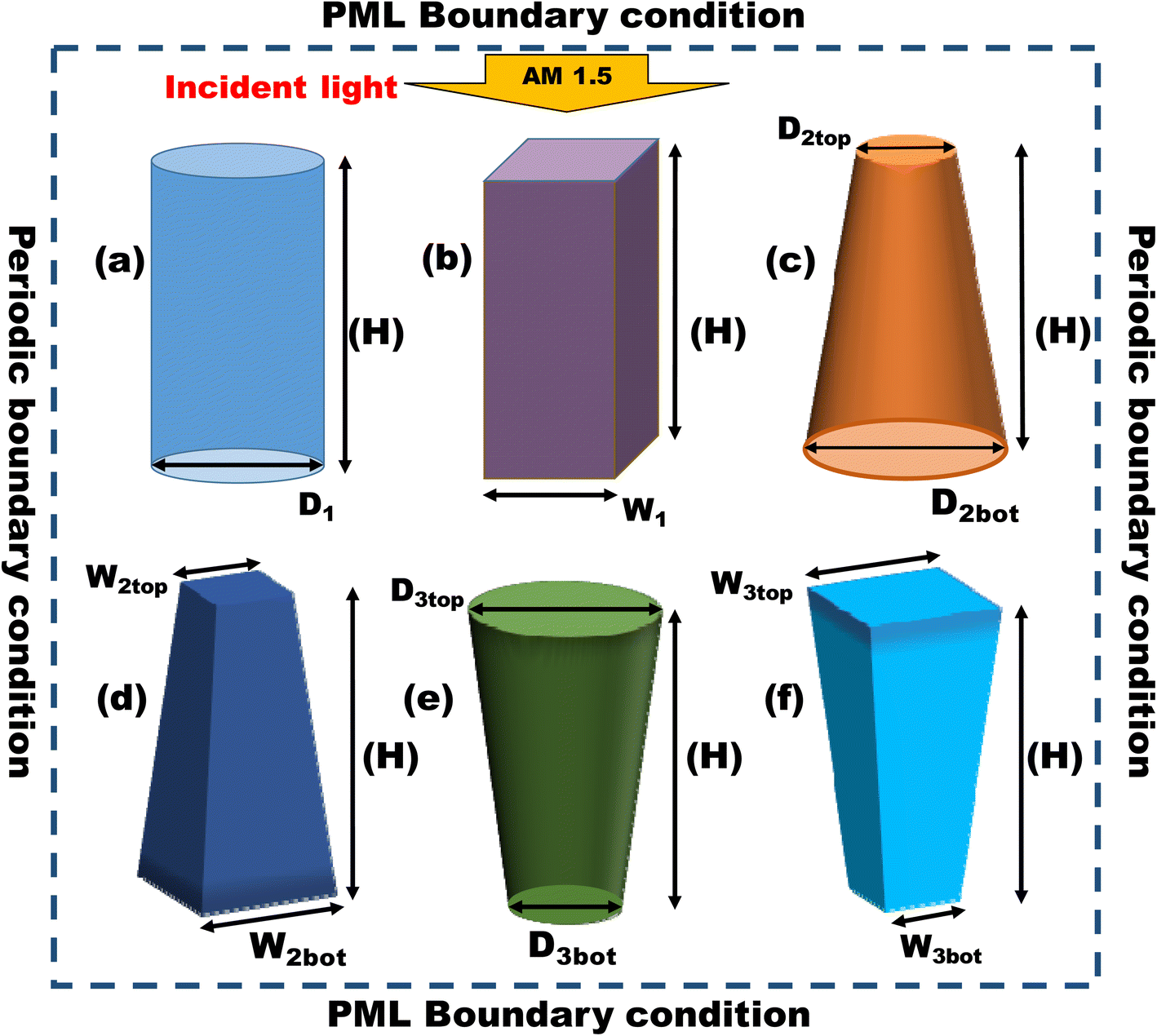
In this article, we have performed an optical analysis of six different nanostructures using the FEM method where we have analyzed optical Jsc, absorptance, and photogeneration rate. The effect of variation of geometric parameters like D, W, Dtop/Dbot, Wtop/Wbot, and FR on optical parameters has also been investigated. The research findings of this article can be helpful in designing efficient nanostructures corresponding to a particular application, bypassing the complexity, cost, and time involved in the fabrication of non-optimized structures. This paper is inscribed in the following manner: Section 1 deals with the basic foundation and motivation for carrying out this research work. In Section 2, we have explained the simulation methodology and structural details of the nanostructures. The results achieved with our simulations on the optimization of nanostructures are discussed in Sections 3 and 4, and we have summarized the research outcomes.
2. Simulation methodology and structure design
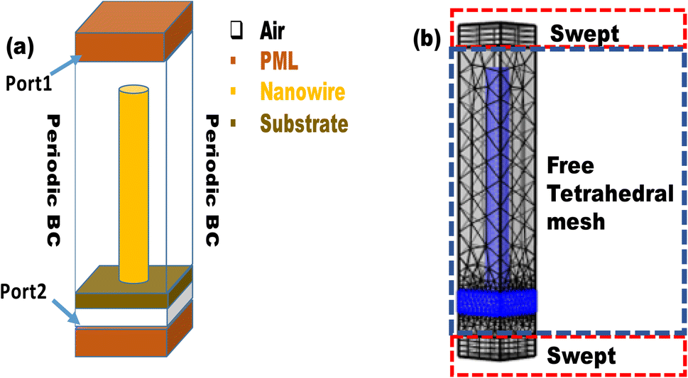
The wave optics module of COMSOL Multiphysics 5.4 is used for the analysis of different nanostructures. COMSOL is based on the finite element method (FEM) which uses the numerical method for solving a partial differential equation. The 3D model has been used for the simulation. The port boundary condition is used on the top and bottom of the nanostructure to launch and receive the electromagnetic wave. PML boundary condition has been used along the z-axis on the top and bottom of the structure in order to avoid the effect of any parasitic reflections in the simulations. Periodic boundary conditions are used along the vertical directions around the nanostructures to ensure the domain could be replicated along both the x and y-axis to construct an array of the unit cell. Helmholtz equation is utilized to calculate electric field intensity which is given as:63| | |
∇ × (∇ × E) − K02εrE = 0
| (1) |
where εr = (n ± ik)2 denotes the dielectric permittivity of the surrounding medium, n is the refractive index and k signifies the extinction coefficient, E is the electric field and K0 is the incident light wave vector. In order to perform optical analysis, values of n and k as a function of wavelength are required, which are extracted from the literature for both Si64 and InP.65 Standard AM1.5 is used as a light source and launched from the top port, considering the transverse electric (TE) and transverse magnetic (TM) modes of polarization. The average of absorptance is calculated by taking the mean of the absorptance in both modes. Absorptance66 as a function of wavelength λ is defined as:| | |
A(λ) = 1 − R(λ) − T(λ)
| (2) |
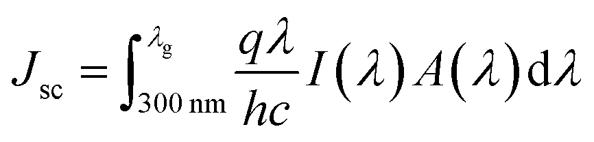
where R (λ) and T (λ) are the reflectance and transmittance obtained from port 2 and port 1 respectively as depicted in Fig. 1(a) and λ is the wavelength that is swept from 300 nm to the cutoff wavelength of the material taken. Optical photocurrent density (Jsc) is defined as:28| |
 | (3) |
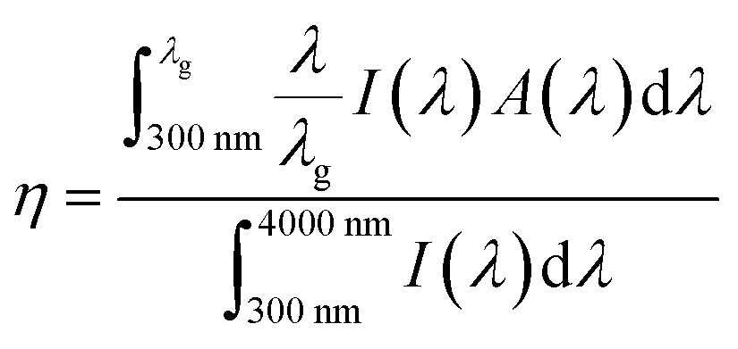
where q is the electronic charge, c is the speed of light, h is Planck's constant, I(λ) is the solar intensity (W m−2 nm−1) under standard air mass 1.5 (AM1.5G) spectrum, and λg is the cut-off wavelength which corresponds to the bandgap of material for Si and InP and are equal to 1130 nm and 930 nm respectively. The maximum short circuit current can be used to compute the ultimate efficiency assuming ideal carrier collection efficiency, which means that each photogenerated carrier is transported efficiently to the respective electrodes, thereby contributing to the photocurrent. The ultimate efficiency is defined as the ratio of the absorbed power to the incident power. Broadband absorption is calculated using the ultimate efficiency,53,67 which is provided by:| |
 | (4) |
 |
| | Fig. 1 (a) Structural details of CNW unit cell (b) meshing details of simulation regions of the unit cell. | |
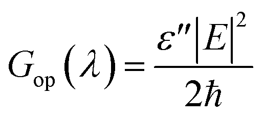
The ultimate efficiency can be described as the maximum possible optical efficiency that can be obtained by an SC under the assumption of unit internal quantum efficiency, that is one electron–hole pair will be generated for each absorbed photon having energy greater than the bandgap of the material and all the generated charges contribute to optical photocurrent without any recombination losses. The lower limit of integration in eqn (3) and (4) is fixed at 300 nm since solar irradiation below this value is insignificant. The photogeneration rate (Gop) at a given λ is computed as given below.63
| |
 | (5) |
where
E is the electric field,
ħ is reduced Planck's constant, and
ε′′ is the imaginary part of permittivity. Setting mesh size is an important step in COMSOL and different mesh element types can be utilized to build a model. Mesh element size should be set correctly in order to achieve good accuracy. The accuracy of finer mesh is high but it requires additional computational time and memory requirements. We must set the maximum mesh element size to
λ/8 or less than the lowest simulated wavelength.
66 In our work, we have chosen swept mesh for the PML region and tetrahedral for the remaining region where the active material is set with finer mesh and the remaining region is set with coarse mesh element type as shown in
Fig. 1(b). Finally, a wavelength sweep is performed with a step size of 10 nm from 300 to the cutoff wavelength (
λg) of the respective material (InP or Si). In
Fig. 2, we have shown a pictorial representation of all the nanostructures used in our analysis. For a better comparison of the characteristics of the nanostructures, the height is taken as 2 μm for all the nanostructures. The parameters such as the
D,
Dtop/
Dbot, and
Wtop/
Wbot, of the structures, are varied in order to obtain optimized dimensions.
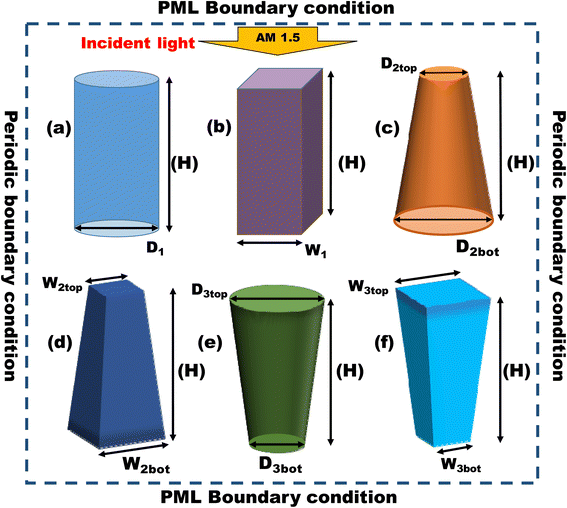 |
| | Fig. 2 (a) CNW, (b) RNW, (c) TNC, (d) TNP, (e) ITNC, and (f) ITNP with height H = 2000 nm. | |
3. Results & discussions
3.1. Optimization of CNW and RNW
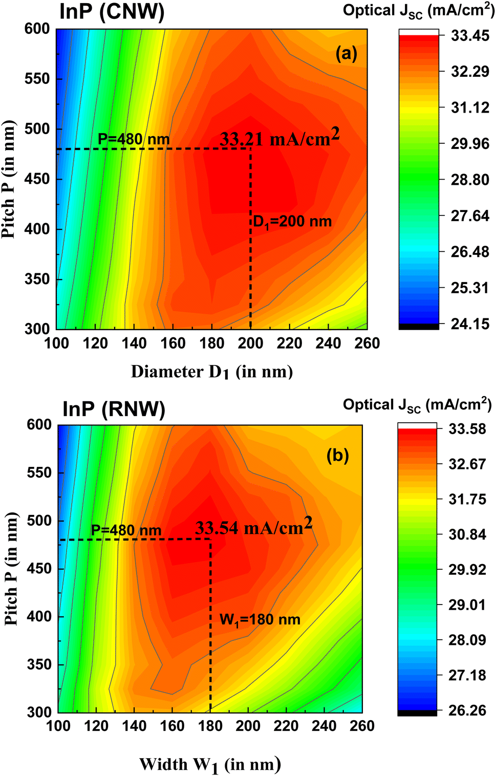
Interaction of photons with nanostructures is dependent on the geometrical dimensions of the NW (D) and the wavelength of light incident on it as it determines the resonant modes that can be supported by the corresponding nanostructures to enhance or diminish light absorption. For this reason, H, D/W of the NW, and FR play an important role in optical absorption. We varied the InP NW H from 500 nm to 3000 nm and we noted that after 2000 nm, the optical Jsc does not change significantly. So, we have fixed the height of the NW H to 2000 nm, considering fabrication feasibility as reported in ref. 29. Initially, we considered the angle of polarization as 0° for both TE and TM mode, and thereafter, we performed a polarization angle-dependent study in Section 3.5. FR of an NW is defined as the ratio of NW area to the pitch (P) area. FR of CNW is πD12/4P2 (ref. 35) where D1 is the diameter of the NW and for RNW FR is W12/P2 where W1 is the width of the RNW. FR variation also shows significant changes in absorptance spectra and it has been observed that high FR gives high absorptance for longer wavelengths whereas low FR gives high absorption in the shorter wavelength regime of absorptance spectra for four different P as shown in Fig. 3(a). As the P is varied keeping D1 constant, we observed that at a lower P, the FR is high leading to high absorption in the long-wavelength region shown by the blue curve P = 280 nm and at low FR for P = 680 nm, high absorption is achieved in low wavelength region shown by the purple curve in Fig. 3(a). But the overall best absorption across the entire wavelength region is achieved at P = 480 nm. P plays a pivotal role in determining the average absorptance of different nanostructures because as we keep P close to D1/W1 of NW, the NWs become closely packed and the incident photons get distributed among the NWs leading to less absorption per NW. Again if we consider the case where P is much greater than D1, then also proper absorption is not achieved because the photons may interact directly with substrate rather than NWs. So we have to select an intermediate pitch where the NWs are able to scatter light such that the light couples with the NW and supports HE1n modes to attain effective absorption.53 We considered a D1 of 200 nm of NW and varied P from 280 nm to 680 nm with a step size of 40 nm in order to see its effect on the optical Jsc in the inset of Fig. 3(a). Note that when P = 280 nm and D1 = 200 nm, optical Jsc is only 30.91 mA cm−2, which clarifies that the NW is not able to capture light efficiently because D is close to P. However, the scenario changes when we consider an optimized P of 480 nm where an optical Jsc of 33.21 mA cm−2 is obtained as compared to an optical Jsc is 31.31 mA cm−2 for P = 640 nm. We have considered a fixed P of 480 nm for all other nanostructures used in our analysis. Thereafter we investigated the effect of D1/W1 on the optical performance of the NW which is determined by the radial resonance mode HE11. We have ignored higher-order modes HE1m because the radius we are considering for NW is small and it prevents the effective coupling of various other guided modes.53 We have plotted the absorptance spectra for four different D1 of 120 nm, 200 nm, 320 nm, and 400 nm and it is clear that the highest absorptance is achieved with D1 = 200 nm. For D1 = 120 nm, absorptance falls sharply after 700 nm which establishes the improper coupling of guided modes with NWs, and a low FR of 0.049 leads to very poor absorption in the long-wavelength region. It can be observed from the inset of Fig. 3(b) that optical Jsc initially increases with an increase in D1 and reaches a maximum value but decreases gradually thereafter, and we obtain a maximum optical Jsc of 33.21 mA cm−2 for D1 = 200 nm and P = 480 nm, which is equivalent to an FR of 0.136 for the CNW.
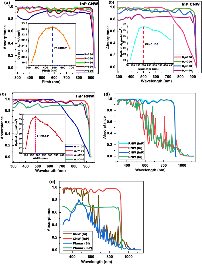 |
| | Fig. 3 Absorptance plot and optical Jsc InP NW (a) at the different P for CNW (b) at different D1 for CNW (c) at different W1 for RNW (d) comparison of both InP RNW and CNW with Si (e) comparison of the CNW with planar structure. | |
A similar procedure of optimization of W1 is followed for the RNW. We have plotted the absorption spectra for four different W1 values of 100 nm, 180 nm, 260 nm, and 340 nm and the nature of the spectra is similar to that of the CNW. In the inset of Fig. 3(c), we have plotted the optical Jsc as a function of W1 and obtained an optimized W1 of 180 nm, FR = 0.141, and optical Jsc of 33.41 mA cm−2 as shown in Fig. 3(c). This is very close to the optimized optical Jsc of CNW 33.2 mA cm−2. For the same dimensions, we have also simulated silicon-based RNW and CNW and compared their performance with the InP counterparts in terms of absorptance and optical Jsc. We found that Si is not able to capture light efficiently after 700 nm as Si being an indirect band gap semiconductor requires phonon assistance and near the wavelength corresponding to its band gap of 1.1 eV show poor absorption characteristics. In addition to this, at higher wavelengths extinction coefficient of Si is low and the interference effect is dominant which leads to the oscillating nature68 in the absorptance plot after 700 nm. However, it has been observed that at low wavelength interference effect is diminished and the absorption increases significantly for NWs, which is shown in Fig. 3(d). Finally, we have compared the absorptance plots of InP and Si CNW with the planar structure where we have considered the H of the nanostructure and of the planar structure to be equal and obtained the absorptance plot as shown in Fig. 3(e). The plot clearly reveals that the use of nanostructure is beneficial as there is a significant increase in the average absorptance. The optical Jsc for InP and Si planar structures is 23.47 mA cm−2 and 13.73 mA cm−2 respectively, which are ∼10 mA cm−2 and ∼5 mA cm−2 less as compared to the corresponding optimized NWs. In Fig. 4, we have plotted a contour map of optical Jsc as a function of P and D1/W1 for the InP CNW and InP RNW respectively. This map helps to find a relation between the geometrical parameters in determining the best optical Jsc.
 |
| | Fig. 4 Contour plot of optical Jsc with the simultaneous variation of P and D1/W1 for (a) InP CNW and (b) InP RNW respectively. The best optical Jsc obtained with both the structures along with the corresponding geometrical dimensions are marked. | |
3.2. Optimization of TNC and TNP
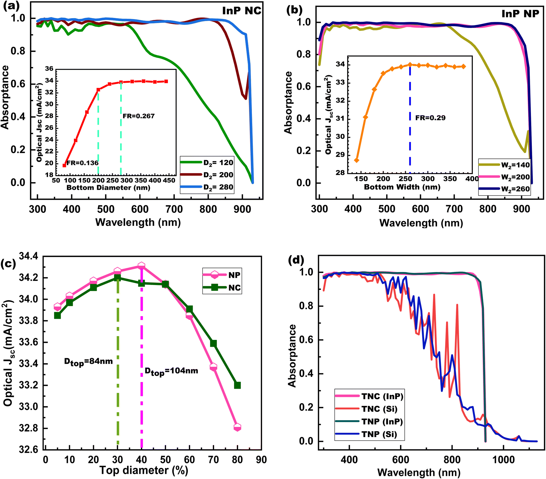
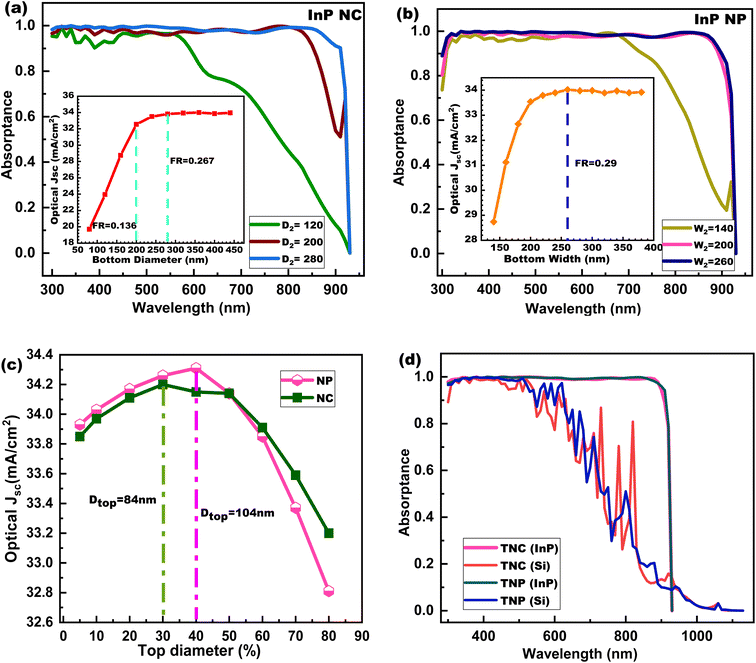
The effect of the variation of P and H of nanostructures significantly affects the optical performance of TNC and TNP as discussed in the previous sections but for a fair comparison between the nanostructures, we have kept the P as 480 nm and H as 2000 nm for both these nanostructures and observed the effect of D2bot/W2bot, D2top/W2top, and FR variation on optical Jsc. FR of TNC and TNP is similar to that of CNW and RNW respectively. Fig. 5(a) shows the absorptance plot of the TNW for three different D2bot of 120 nm, 200 nm, and 280 nm. Note that higher average absorptance is obtained for a D2bot of 280 nm as more optical resonance modes are supported by the TNW with this dimension. For D2bot above 200 nm, the absorptance is close to unity over a broader range of the spectrum showing the superior absorbing capability of the structures. The reason for the nearly perfect absorption of TNC and TNP is because of their graded refractive index profile along the length which helps in supporting a higher number of resonant modes in comparison to NWs.55 Moreover, the lesser top surface area of these structures compared to the bottom helps in less reflection and transmission losses. It has been reported that in NC and NP, HE11 and HE12 modes are responsible for enhanced absorptance.69 We have varied the D2bot of the NC from 80 nm to 440 nm by keeping the D2top of NC as 5% of D2bot initially. It has been observed that an NC with D2bot of 80 nm is not able to couple the light efficiently in higher wavelength regions limiting the optical Jsc to 19.71 mA cm−2 only but as we increase the D2bot, there is a sharp increase in optical Jsc up to 200 nm, after which it increases slowly up to 280 nm and saturates thereafter as shown in the inset of Fig. 5(a). For the NC, we have considered an optimized D2bot of 280 nm with FR of 0.26 rather than 320 nm as there is a negligible increase in optical Jsc beyond 280 nm. The absorptance plot for the InP NP for three different W2bot of 140 nm, 200 nm, and 260 nm depicted in Fig. 5(b) shows an almost identical nature to that of the NC. A similar procedure for optimization has been followed for NP as stated above and an optimum W2bot of 260 nm is obtained at FR of 0.29 with optical Jsc of 33.9 mA cm−2 as shown in the inset of Fig. 5(b), which shows the variation of optical Jsc as a function of the W2bot of the NP. As the FR for optimized D2bot/W2bot comes within the range of 0.25–0.30, no significant change in optical Jsc is observed on increasing FR. Additionally, when we consider the D2top/W2top very small compared to the D2bot/W2bot, the resultant pointed structure results in diffraction or multiple reflections of the incident light between two adjacent NC or NP and absorbed finally but, in this process, there is a fair amount of chance that the light reaches substrate and get transmitted back to air. Thus, we have tried to simulate the effect of D2top/W2top variation for both structures on optical Jsc. It is observed that on increasing the D2top/W2top from 0 to 90% of the D2bot/W2bot, optical Jsc initially increases and reaches a maximum value but it decreases thereafter as shown in Fig. 5(c). Initially, as the D2top/W2top is very less, the absorption of a photon is less due to the pointed structure but when we increase the D2top/W2top to 30 or 40%, the increase in the top surface area leads to better photon absorption capability of the nanostructures. Further increase in D2top/W2top leads to the dominating effect of surface reflection of photons in comparison to absorption, which leads to a decrease in optical Jsc as is demonstrated in Fig. 5(c). The optical Jsc of both the optimized structures is almost the same and equal to ∼34.2 mA cm−2. The same dimensions have been considered for computing the absorptance spectra of Si-based TNC and TNP to perform a comparative analysis with InP nanostructures as shown in Fig. 5(d). While Si-based TNC and TNP exhibit nearly the same absorptance profile in lower wavelength regions, there is a slight increase in the magnitude of the peaks for TNC and TNP with respect to NW in the wavelength region between 500 to 800 nm which leads to an increase in optical Jsc.
 |
| | Fig. 5 Absorptance plot and optical Jsc (a) at different D2bot for NC (b) at different W2bot for NP (c) D2top/W2top variation for both NC and NP (d) comparison of both InP TNC and TNP with Si. | |
3.3. Optimization of ITNC and ITNP
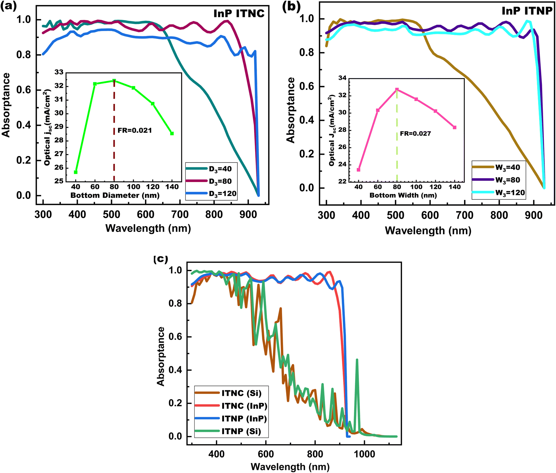
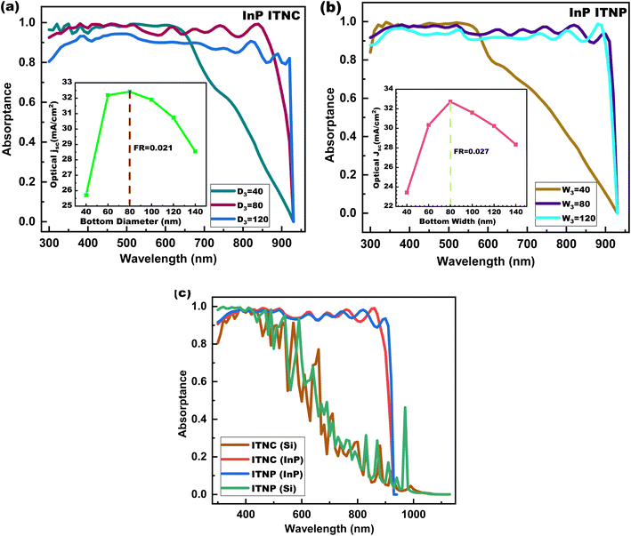
TNC and TNP structures exhibit superior antireflection properties and broadband absorption spectrum but as far as an SC is concerned, it should be able to reflect more light in the infrared (IR) region. Although the percentage of IR waves reaching the earth's surface is very less compared to the visible wavelength region, it has a severe impact on device performance. IR waves entering into the SCs can be absorbed by the metal contacts leading to a heating effect and degradation of the device performance.58 In order to achieve higher reflection for longer wavelengths, we have performed an analysis on ITNC and ITNP which also offers a graded refractive index profile where a high refractive index is at the top and it decreases gradually towards the bottom of the structure.55 As D3top/W3top is more than D3bot/W3bot it offers more reflection in higher wavelength regions. We have fixed the P and H of the nanostructure as 480 nm and 2000 nm respectively and kept the same aspect ratio between D3top/D3bot and W3top/W3bot as we attained for TNC and TNP and simply inverted the structures. For ITNC, we fixed the aspect ratio to 3.33, which means that the D3top is 3.33 times the D3bot. Similarly, we consider an aspect ratio of 2.5 for ITNP, which is similar to TNP, and swapped the W3top with W3bot and vice versa. In Fig. 6(a) and (b), we have plotted the absorption spectrum for the ITNC and ITNP respectively with corresponding D3bot/W3bot of 40 nm, 80 nm, and 120 nm. A similar pattern in the absorptance profile is observed for both structures. When we compare the absorptance spectra of ITNC and ITNP with NWs and TNC and TNP, we can see that, unlike NWs, TNC and TNP, the inverted structures provide lesser absorptance or higher reflectance for longer wavelengths beyond 750 nm which can be confirmed from the oscillatory nature in the spectra. We varied the D3bot/W3bot of both nanostructures from 40 nm to 140 nm by maintaining their respective aspect ratios. We observed a sharp increase in optical Jsc from 25.71 mA cm−2 to 32.1 mA cm−2 as an increase in the D3bot from 40 nm to 60 nm for ITNC as shown in the inset of Fig. 6(a). We increased the D3bot further and obtained an optimized value at 80 nm for ITNC at FR of 0.021 and optical Jsc of 32.43 mA cm−2 and for ITNP, we achieved an optimized D3bot of 80 nm, FR of 0.027, and optical Jsc of 32.73 mA cm−2 as shown in the inset of Fig. 6(a) and (b) respectively. In Fig. 6(c), we have compared the absorptance spectra of the optimized InP inverted nanostructures with Si-based nanostructures. From the absorptance spectra, we have computed the optical Jsc and it can be concluded that the optical Jsc of Si ITNC and ITNP of 17.69 mA cm−2 and 18.49 mA cm−2 respectively are much smaller in comparison to the optical Jsc of the corresponding InP nanostructures. For a fair comparison of the optical performance of different InP and Si-based nanostructures, we have listed the optical Jsc in Table 1. A comparative analysis of optical Jsc, ultimate efficiency, and average absorptivity of the six proposed nanostructures in this manuscript with InP and Si-based nanostructures available in the literature is performed in Table 2. It is evident from the table that the optical Jsc of uncoated InP TNP and TNC are almost comparable to that of coated (Ta2O5/ZnO) InP nanostructures. The reason for this improved performance is mainly due to the enhanced broadband absorption achieved with these nanostructures.
 |
| | Fig. 6 Absorptance plot and optical Jsc (a) at different D3bot for ITNC (b) at different W3bot ITNP (c) comparison of both InP ITNC and ITNP with Si. | |
Table 1 Optical Jsc of various InP and Si nanostructures
| Nanostructures |
Optical Jsc (mA cm−2) |
| InP |
Si |
| CNW |
33.21 |
18.85 |
| RNW |
33.54 |
18.82 |
| TNC |
34.21 |
23.24 |
| TNP |
34.28 |
23.73 |
| ITNC |
32.43 |
17.69 |
| ITNP |
32.73 |
18.49 |
| Planar structure |
23.47 |
13.73 |
Table 2 Comparison of optical Jsc, ultimate efficiency, and average absorptivity of the proposed nanostructures with other nanostructures available in the literature
| Structures |
Geometrical dimensions |
Optical Jsc (mA cm−2) |
Ultimate efficiency %) |
Average absorptivity (%) |
References |
| InP CNW |
H = 2 μm |
33.21 |
44.59 |
96.3 |
This work |
| FR = 0.136 |
| D1 = 200 nm |
| InP RNW |
H = 2 μm |
33.54 |
44.85 |
95.6 |
This work |
| FR = 0.44 |
| W1 = 180 nm |
| InP TNC |
H = 2 μm |
34.21 |
45.81 |
97.4 |
This work |
| FR = 0.26 |
| D2top = 84 nm |
| D2bot = 280 nm |
| InP TNP |
H = 2 μm |
34.28 |
46.01 |
97.2 |
This work |
| FR = 0.29 |
| W2top = 104 nm |
| W2bot = 260 nm |
| InP ITNC |
H = 2 μm |
32.43 |
43.53 |
93.2 |
This work |
| FR = 0.021 |
| D3top = 266 nm |
| D3bot = 80 nm |
| InP ITNP |
H = 2 μm |
32.73 |
43.96 |
93.1 |
This work |
| FR = 0.027 |
| W3top = 200 nm |
| W3bot = 80 nm |
| Si nanopillar |
Height = 2 μm |
— |
— |
87.7 |
70 |
| Pitch = 1.27 μm |
| InP nanowire |
Height = 2 μm |
|
|
94 |
36 |
| Pitch = 400 nm |
| Cylindrical InP nanowire |
Height = 2 μm |
31.08 |
— |
— |
35 |
| Diameter = 200 nm |
| Rectangular InP nanowire |
Height = 2 μm |
31.7 |
— |
— |
35 |
| Width = 180 nm |
| Ta2O5 coated cylindrical/rectangular nanowire |
Height = 2 μm |
34.88 |
— |
— |
35 |
| Diameter = 200 nm |
| Width = 180 nm |
| InP radial nanowire |
Height = 2 μm |
29.4 |
— |
— |
33 |
| Pitch = 480 |
| Diameter = 80 nm |
| ZnO coated InP radial nanowire |
Height = 2 μm |
32.4 |
— |
— |
33 |
| Pitch = 480 |
| Oxide shell = 90 nm |
| Core diameter = 80 nm |
| AZO/ZnO coated radial junction nanowire |
Length = 2 μm |
31.2 |
— |
— |
71 |
| Pitch = 1 μm |
| FR = 0.13 |
3.4. Electric field and photogeneration rate profiles
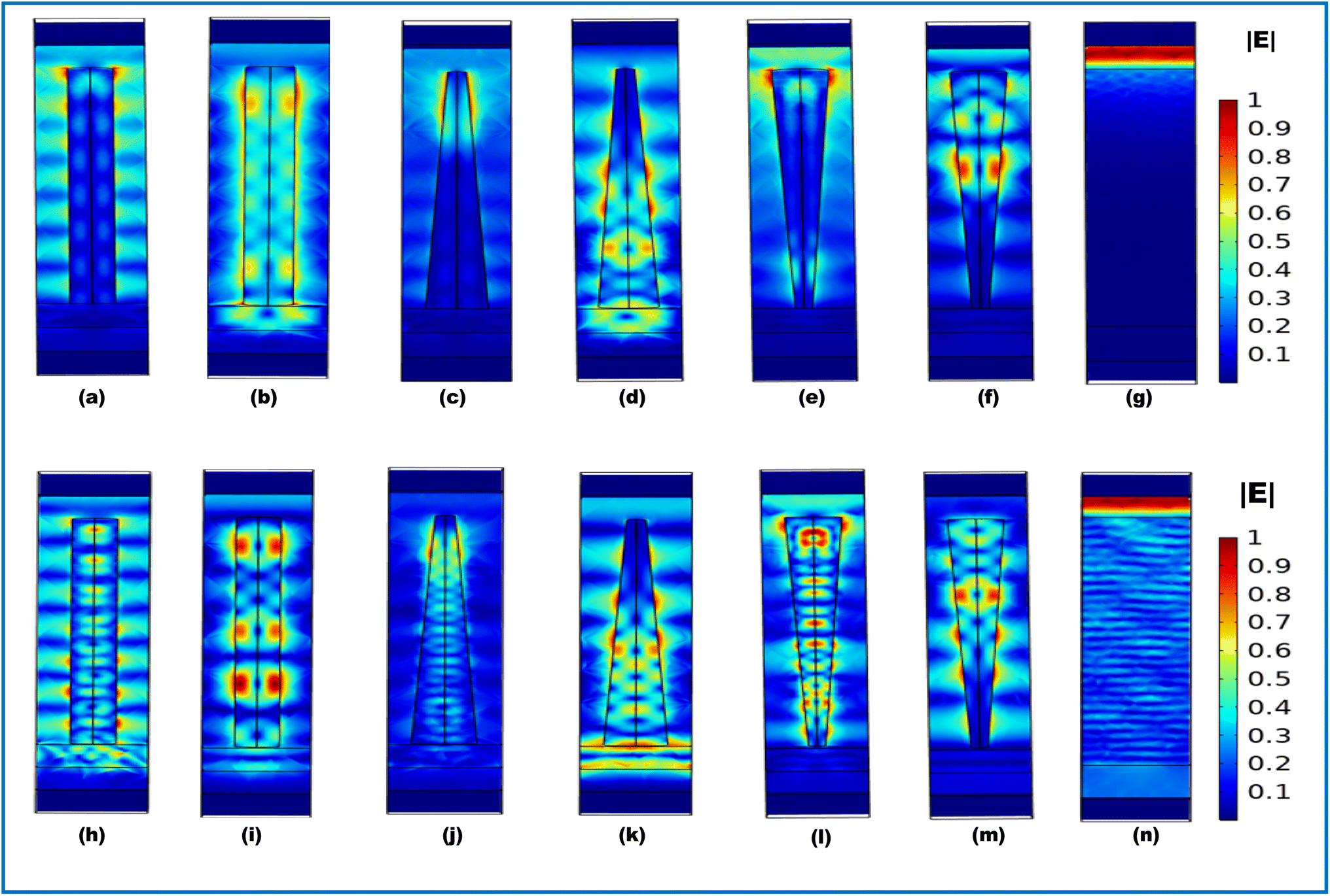
We have also simulated the normalized electric field profiles of CNW, TNC, ITNC, and planar structures at λ = 600 nm and 920 nm for both InP and Si. It has been observed that the electric field profiles and the photogeneration rates for the other nanostructures namely the RNW, TNP, and ITNP are similar to CNW, TNC, and TNP for both wavelengths. Therefore, in order to avoid repetitive analysis and redundant data, we have considered only one set of nanostructures. For CNW, it can be observed from Fig. 7(a) that the electric field is mostly concentrated at the top of the CNW and reduces as we go down the length of the CNW with the majority of the absorption exhibited by the upper half of the CNW for λ = 600 nm. However, for λ = 920 as shown in Fig. 7(b), the spreading of the electric field across the entire CNW occurs and some of the photons are also transmitted to the substrate, which causes a sharp decline in the absorption spectra beyond 920 nm as is depicted in the absorptance plots in Fig. 3(e). In the case of Si, the electric field profiles for both the wavelengths plotted in Fig. 7(h) and (i) respectively show a series of maxima and minima along the entire length of the CNW reaches the substrate also, which is responsible for the poor absorbing capability of Si nanostructures in comparison to the InP counterparts. For TNC, it can be observed from the normalized electric field profiles plotted in Fig. 7(c), that the electric field is confined within the upper half of the TNC and very less spreading occurs towards the bottom of TNC for λ = 600 nm. In addition to this, the spreading of the electric field in the region between the TNC is lesser than that of NWs. For λ = 920 nm (Fig. 7(d)), the electric field is mostly concentrated in the lower half of the TNC and is also transmitted to the substrate similar to that of NW. For Si at λ = 600 nm (Fig. 7(j)), the electric field profile is distributed along the entire TNC unlike that of InP. However, for λ = 920 nm (Fig. 7(k)), the profile is similar to that of InP. The electric field profile for ITNC at λ = 600 nm shown in Fig. 7(e) reveals that the field is mostly confined on the top of the nanostructure in the case of InP with minor intensity at the bottom of the nanostructure. However, at λ = 920 nm, the electric field shown in Fig. 7(f) is distributed mostly in the upper half of the nanostructure with zero electric fields penetrating into the substrate. In the case of Si, the electric field distribution for both the wavelengths shown in Fig. 7(l) and (m) contains a series of maxima and minima along the nanostructure without reaching the substrate, resulting in zero transmittivity. Hence, it can be concluded that the inverted structures almost exhibit smaller absorptance than the NW or NC structures but higher reflectivity, especially in the IR region. The electric filed profiles for InP and Si planar structure plotted in Fig. 7(g) and (n) respectively clearly show that the electric field is transmitted to the substrate in the case of Si, which results in transmittivity loss and lower absorption in comparison to that of InP, where the electric field is confined mostly in the absorber layer.
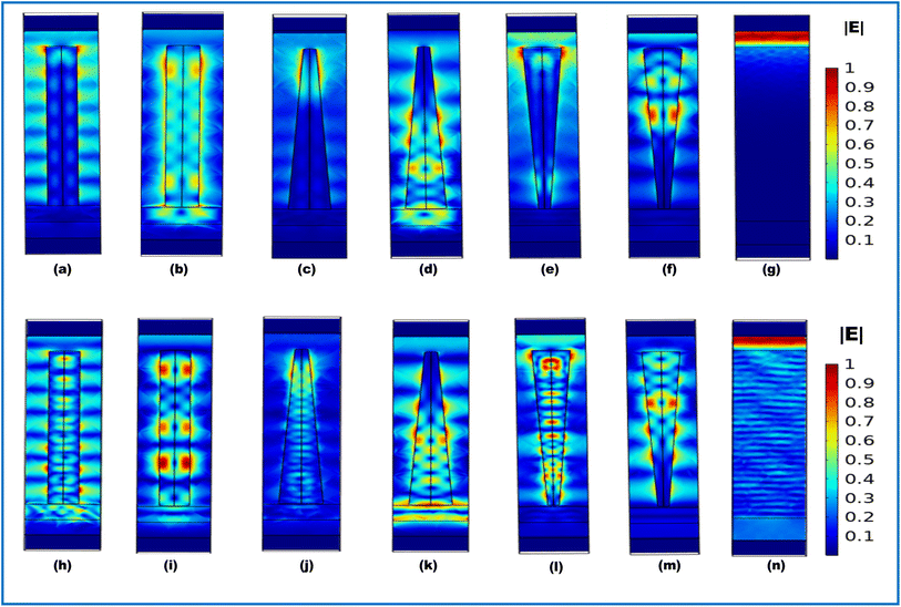 |
| | Fig. 7 Electric field for CNW, TNC, INTC, and planar at λ = 600 nm for InP (a, c, e and g) and Si (h, j, l and n) and at λ = 920 nm for InP (b, d and f) and Si (i, k and m). | |
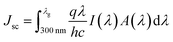
We have computed the photogeneration rate profiles of the nanostructures for both InP (Fig. 8(a–g)) and Si (Fig. 8(h–n)) for wavelengths of λ = 600 and λ = 920 nm. The photogeneration rate is proportional to the square of the electric field magnitude and so the distribution of the photogenerated carriers exhibits similar nature. However, it can be observed from the profiles that the photogeneration rate for all the InP-based structures is higher than that of Si, which would surely produce a better photovoltaic performance of the InP-based SCs. In order to provide a deeper insight into the photogenerated response of different nanostructures, the maximum photogeneration rate of the different nanostructures is listed in Table 3.
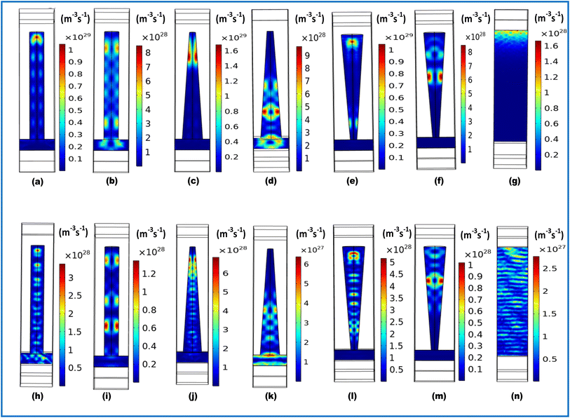 |
| | Fig. 8 Photogeneration rate for CNW, TNC, INTC, and planar at λ = 600 nm InP (a, c, e and g) and Si (h, j, l and n) and at λ = 920 nm for InP (b, d and f) and Si (i, k and m). | |
Table 3 Maximum photogeneration rate of various InP and Si nanostructures
| Nanostructures |
Maximum photogeneration rate (m−3 s−1) |
| λ = 600 nm |
λ = 920 nm |
| InP |
Si |
InP |
Si |
| CNW |
1 × 1029 |
3 × 1028 |
8 × 1028 |
1.2 × 1028 |
| TNC |
1.6 × 1029 |
6 × 1028 |
9 × 1028 |
6 × 1027 |
| ITNC |
1 × 1029 |
5 × 1028 |
8 × 1028 |
1 × 1028 |
| Planar structure |
1.6 × 1028 |
2.5 × 1027 |
2.6 × 1027 |
2.3 × 1026 |
3.5. Effect of the change in the angle of incidence
To see the effect of the variation of the angle of incidence of the electromagnetic waves on the optical performance of the nanostructures, we have plotted the variation of ultimate efficiency (η) computed using eqn (3) as a function of the angle of incidence. We have performed this analysis for the optimized nanostructures for both transverse TE and TM modes of plane-polarized incident light. Note that for TE mode, the electric field is perpendicular to the plane of incidence whereas in TM mode the electric field component is parallel to the plane of incidence.72,73 We have also plotted η by taking the mean value of both the TE and TM modes. For both Si and InP CNW and RNW, η shown in Fig. 9(a) and (b) respectively show negligible variation with the angle of incidence. For InP, η decreases beyond 20° and for Si, there is a slight increase in η up to 40° and it decreases thereafter. A similar pattern in the variation of η with the angle of incidence for InP NWs has been reported in ref. 72. Unlike NWs, the TNC and TNP exhibit slightly higher values of η in TM mode for angles of incidence greater than 20° as is evident from Fig. 9(c) and (d) respectively. This is due to the fact that TM mode being parallel to the nanostructure facilitates more interaction of the incident photons with the nanostructures due to the graded refractive index profile, thereby resulting in improved absorption and ultimate efficiency as compared to NWs. The obtained results for Si with somewhat different geometrical parameters have shown the same nature as in ref. 74. For ITNC and ITNP, it can be observed from Fig. 9(e) and (f) that for angles less than 30°, there is not much difference in η between TE and TM modes. For angles of incidence greater than 40°, η for TE mode is more dominant than TM mode. This is because of the reverse nature of the refractive index profile for the ITNC and ITNP in comparison to the TNC and TNP which results in better interaction of TE mode with the inverted nanostructures.73
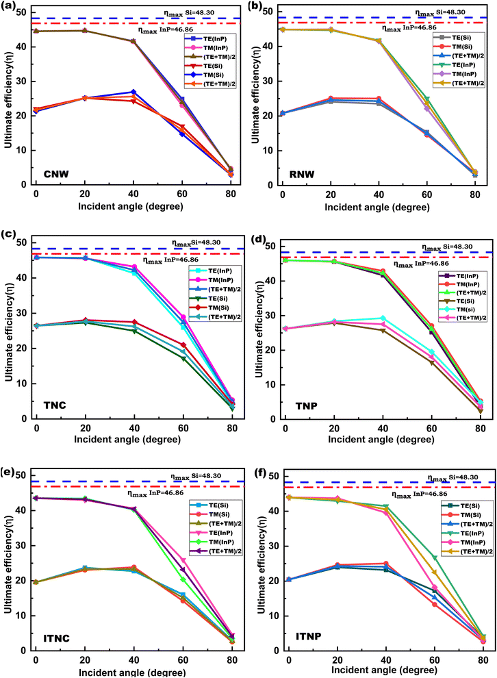 |
| | Fig. 9 Variation of ultimate efficiency (η) with respect to the angle of incidence for (a) CNW, (b) RNW, (c) TNC, (d) TNP, (e) ITNC, and (f) ITNP. | |
4. Conclusions
In summary, an analysis of six different nanostructures is performed and the effect of the variations in D/W, P, and FR are investigated and compared in terms of the optical Jsc, absorptance, electric field, and photogeneration rate (Gop) of each nanostructure. It is observed that InP-based SC outperforms Si-based SC nanostructures. While the maximum optical Jsc for InP TNP is 34.28 mA cm−2, for Si the corresponding nanostructure gives only 23.73 mA cm−2. It can be established that optical Jsc for CNW and RNW, TNC and TNP, and ITNC and ITNP are almost similar, which indicates that there is a negligible effect of the edges of the nanostructures on their optical performance. The optical Jsc of inverted type nanostructure is slightly less than the other nanostructures with the added advantage of almost zero transmittivity and higher reflectance in the longer wavelength regime minimizing the radiation losses in SCs. The effect of the angle of incidence on the η of various nanostructures for TE, TM, and the mean of TE and TM modes has also been investigated. It can be concluded from this analysis that InP-based nanostructures exhibit better optical efficiency in comparison to that Si. The computed results from this analysis can provide valuable insights into the optical performance of the different investigated nanostructures to proceed with the fabrication of these nanostructures for incorporation in the active layer of SCs.
Data availability
The raw/processed data required to reproduce these findings cannot be shared at this time as the data also forms part of an ongoing study.
Conflicts of interest
The authors declare that they have no known competing financial interests or personal relationships that could have appeared to influence the work reported in this paper.
Acknowledgements
The authors are thankful for the financial support received from DST SERB vide Grant No. ECR/2017/002369 for this research on III–V nanostructure-based solar cells.
References
- X. Costoya, M. DeCastro, D. Carvalho, B. Arguilé-Pérez and M. Gómez-Gesteira, Renewable Sustainable Energy Rev., 2022, 157, 112037 CrossRef.
- M. B. Hayat, D. Ali, K. C. Monyake, L. Alagha and N. Ahmed, Int. J. Energy Res., 2019, 43, 1049–1067 CrossRef.
- N. Kannan and D. Vakeesan, Renewable Sustainable Energy Rev., 2016, 62, 1092–1105 CrossRef.
- M. K. Hossain, G. F. I. Toki, I. Alam, R. Pandey, D. P. Samajdar, M. F. Rahman, M. R. Islam, M. H. K. Rubel, H. Bencherif, J. Madan and M. K. A. Mohammed, New J. Chem., 2023, 47, 4801–4817 RSC.
- S. Sharma, K. K. Jain and A. Sharma, Mater. Sci. Appl., 2015, 06, 1145–1155 CAS.
- M. K. Hossain, M. H. K. Rubel, G. F. I. Toki, I. Alam, M. F. Rahman and H. Bencherif, ACS Omega, 2022, 7, 43210–43230 CrossRef CAS PubMed.
- H. Bencherif and M. K. Hossain, Sol. Energy, 2022, 248, 137–148 CrossRef CAS.
- M. K. Hossain, D. P. Samajdar, R. C. Das, A. A. Arnab, M. F. Rahman, M. H. K. Rubel, M. R. Islam, H. Bencherif, R. Pandey, J. Madan and M. K. A. Mohammed, Energy Fuels, 2023, 37, 3957–3979 CrossRef CAS.
- M. Konagai, Jpn. J. Appl. Phys., 2011, 50, 030001 CrossRef.
- M. K. Hossain, G. F. I. Toki, A. Kuddus, M. H. K. Rubel, M. M. Hossain, H. Bencherif, M. F. Rahman, M. R. Islam and M. Mushtaq, Sci. Rep., 2023, 13, 2521 CrossRef CAS PubMed.
- M. K. Hossain, A. A. Arnab, R. C. Das, K. M. Hossain, M. H. K. Rubel, M. F. Rahman, H. Bencherif, M. E. Emetere, M. K. A. Mohammed and R. Pandey, RSC Adv., 2022, 12, 34850–34873 RSC.
- V. K. Narasimhan and Y. Cui, Nanophotonics, 2013, 2, 187–210 CrossRef CAS.
- M. C. Beard, J. M. Luther and A. J. Nozik, Nat. Nanotechnol., 2014, 9, 951–954 CrossRef CAS PubMed.
- S. Khan and M. K. Hossain, in Nanoparticle-Based Polymer Composites, Elsevier, 2022, pp. 15–54 Search PubMed.
- Y. Ren, Q. Chen, M. He, X. Zhang, H. Qi and Y. Yan, ACS Nano, 2021, 15, 6105–6128 CrossRef CAS PubMed.
- Y. Ren, Y. Yan and H. Qi, Adv. Colloid Interface Sci., 2022, 308, 102753 CrossRef CAS PubMed.
- V. S. Vendamani, S. V. S. N. Rao, A. P. Pathak and V. R. Soma, ACS Appl. Nano Mater., 2022, 5, 4550–4582 CrossRef CAS.
- R. Z. A. Manj, X. Chen, W. U. Rehman, G. Zhu, W. Luo and J. Yang, Front. Chem., 2018, 6, 1–14 CrossRef PubMed.
- N. Fukata, T. Subramani, W. Jevasuwan, M. Dutta and Y. Bando, Small, 2017, 13, 1–13 Search PubMed.
- P. Mushonga, M. O. Onani, A. M. Madiehe and M. Meyer, J. Nanomater., 2012, 2012, 869284 Search PubMed.
- H. Li, C. Jia, X. Meng and H. Li, Front. Chem., 2019, 7, 1–15 CrossRef PubMed.
- V. E. Ferry, A. Polman and H. A. Atwater, ACS Nano, 2011, 5, 10055–10064 CrossRef CAS PubMed.
- M. L. Brongersma, Y. Cui and S. Fan, Nat. Mater., 2014, 13, 451–460 CrossRef CAS PubMed.
- E. Garnett and P. Yang, Nano Lett., 2010, 10, 1082–1087 CrossRef CAS PubMed.
- S. Kumar Agnihotri, D. V. Prashant and D. P. Samajdar, Sol. Energy, 2022, 237, 293–300 CrossRef CAS.
- B. Wang, E. Stevens and P. W. Leu, Opt. Express, 2014, 22, A386 CrossRef PubMed.
- S. Jeong, E. C. Garnett, S. Wang, Z. Yu, S. Fan, M. L. Brongersma, M. D. McGehee and Y. Cui, Nano Lett., 2012, 12, 2971–2976 CrossRef CAS PubMed.
- Z. Xu, H. Huangfu, X. Li, H. Qiao, W. Guo, J. Guo and H. Wang, Opt. Commun., 2016, 377, 104–109 CrossRef CAS.
- S. K. Agnihotri, D. P. Samajdar and Z. Arefinia, Design of InP-based truncated nanopyramid solar cells with conformal coating of PEDOT: PSS for improved light harvesting efficiency, Elsevier B.V., 2020, vol. 110 Search PubMed.
- D. V. Prashant, D. P. Samajdar and Z. Arefinia, IEEE Trans. Electron Devices, 2021, 68, 1135–1141 CAS.
- S. Vishwakarma and D. P. Samajdar, Sol. Energy, 2019, 190, 278–285 CrossRef.
- M. K. Basher, M. Khalid Hossain, R. Afaz, S. Tayyaba, M. A. R. Akand, M. T. Rahman and N. M. Eman, Results Phys., 2018, 10, 205–211 CrossRef.
- V. Raj, L. Fu, H. H. Tan and C. Jagadish, IEEE J. Photovoltaics, 2019, 9, 980–991 Search PubMed.
- S. K. Agnihotri, D. P. Samajdar and D. V. Prashant, IEEE Trans. Electron Devices, 2021, 68, 5666–5673 CAS.
- S. K. Agnihotri, D. P. Samajdar, D. V. Prashant and Z. Arefinia, Opt. Mater., 2021, 119, 111365 CrossRef CAS.
- N. Anttu, A. Abrand, D. Asoli, M. Heurlin, I. Åberg, L. Samuelson and M. Borgström, Nano Res., 2014, 7, 816–823 CrossRef CAS.
- L. Liu, Y. Diao, Z. Lv and Y. Sun, Mater. Res. Bull., 2021, 141, 111364 CrossRef CAS.
- M.-D. Ko, T. Rim, K. Kim, M. Meyyappan and C.-K. Baek, Sci. Rep., 2015, 5, 11646 CrossRef PubMed.
- S. E. Han and G. Chen, Nano Lett., 2010, 10, 1012–1015 CrossRef CAS PubMed.
- C. Deng, X. Tan, L. Jiang, Y. Tu, M. Ye and Y. Yi, Opt. Commun., 2018, 407, 199–203 CrossRef CAS.
- W. Qarony, M. I. Hossain, M. K. Hossain, M. J. Uddin, A. Haque, A. R. Saad and Y. H. Tsang, Results Phys., 2017, 7, 4287–4293 CrossRef.
- M. I. Hossain, W. Qarony, M. K. Hossain, M. K. Debnath, M. J. Uddin and Y. H. Tsang, Appl. Nanosci., 2017, 7, 489–497 CrossRef CAS.
- N. Anttu, Opt. Lett., 2013, 38, 730 CrossRef PubMed.
- M. Bosi and C. Pelosi, Prog. Photovoltaics Res. Appl., 2007, 15, 51–68 CrossRef CAS.
- Z. Zhang, J. Zhou, Y. Wu, Z. Xia and X. Qin, Appl. Phys. Lett., 2020, 116, 113903 CrossRef CAS.
- D. J. Brinker and I. Weinberg, in 22nd Intersociety Energy Conversion Engineering Conference, American Institute of Aeronautics and Astronautics, Reston, Virginia, 1987 Search PubMed.
- M. K. Hossain, S. Hossain, M. H. Ahmed, M. I. Khan, N. Haque and G. A. Raihan, ACS Appl. Electron. Mater., 2021, 3, 3715–3746 CrossRef CAS.
- M. F. Pervez, M. N. H. Mia, S. Hossain, S. M. K. Saha, M. H. Ali, P. Sarker, M. K. Hossain, M. A. Matin, M. Hoq and M. A. M. Chowdhury, Optik, 2018, 162, 140–150 CrossRef CAS.
- M. K. Hossain, M. T. Rahman, M. K. Basher, M. J. Afzal and M. S. Bashar, Results Phys., 2018, 11, 1172–1181 CrossRef.
- E. U. Onyegam, J. Mantey, R. A. Rao, L. Mathew, M. Hilali, S. Saha, D. Jawarani, S. Smith, D. A. Ferrer, S. V. Sreenivasan and S. K. Banerjee, in 2011 37th IEEE Photovoltaic Specialists Conference, IEEE, 2011, pp. 000271–000273 Search PubMed.
- G. Barbarino, R. De, G. De, C. Maximiliano, S. Russo and D. Vivolo, in Photodiodes - World Activities in 2011, InTech, 2011 Search PubMed.
- M. A. Green, Y. Hishikawa, E. D. Dunlop, D. H. Levi, J. Hohl-Ebinger and A. W. Y. Ho-Baillie, Prog. Photovoltaics Res. Appl., 2018, 26, 3–12 CrossRef.
- N. Anttu and H. Q. Xu, Opt. Express, 2013, 21, A558 CrossRef CAS PubMed.
- K. T. Fountaine, C. G. Kendall and H. A. Atwater, Opt. Express, 2014, 22, A930 CrossRef CAS PubMed.
- T.-H. Pei, S. Thiyagu and Z. Pei, Appl. Phys. Lett., 2011, 99, 153108 CrossRef.
- X. Yuan, D. Pan, Y. Zhou, X. Zhang, K. Peng, B. Zhao, M. Deng, J. He, H. H. Tan and C. Jagadish, Appl. Phys. Rev., 2021, 8, 021302 CAS.
- W. Kim, L. Güniat, A. Fontcuberta I Morral and V. Piazza, Appl. Phys. Rev., 2021, 8, 011304 CAS.
- H. Butt, Q. Dai, R. Rajasekharan, T. D. Wilkinson and G. A. J. Amaratunga, Appl. Phys. Lett., 2011, 99, 133105 CrossRef.
- M. Yao, N. Huang, S. Cong, C. Y. Chi, M. A. Seyedi, Y. T. Lin, Y. Cao, M. L. Povinelli, P. D. Dapkus and C. Zhou, Nano Lett., 2014, 14, 3293–3303 CrossRef CAS PubMed.
- M. Piralaee, A. Asgari and V. Siahpoush, Physics Letters, Section A: General, Atomic and Solid State Physics, 2017, 381, 489–493 CrossRef CAS.
- G. Shalev, S. W. Schmitt, H. Embrechts, G. Brönstrup and S. Christiansen, Sci. Rep., 2015,(5), 1–7 Search PubMed.
- S. Yu, G. Miao, Y. Jin, L. Zhang, H. Song, H. Jiang, Z. Li, D. Li and X. Sun, Phys.
E, 2010, 42, 1540–1543 CrossRef CAS.
- H. Abedini-Ahangarkola and S. Soleimani-Amiri, Int. J. Eng., 2021, 34, 873–880 Search PubMed.
- C. Schinke, P. Christian Peest, J. Schmidt, R. Brendel, K. Bothe, M. R. Vogt, I. Kröger, S. Winter, A. Schirmacher, S. Lim, H. T. Nguyen and D. MacDonald, AIP Adv., 2015, 5, 067168 CrossRef.
- S. Adachi, J. Appl. Phys., 1989, 66, 6030–6040 CrossRef CAS.
- X. Zhangyang, L. Liu, Z. Lv, F. Lu and J. Tian, J. Nanopart. Res., 2020, 22, 243 CrossRef CAS.
- C. Lin and M. L. Povinelli, in Optics InfoBase Conference Papers, ed. L. Tsakalakos, 2010, vol. 17, p. 77721G Search PubMed.
- L. Hu and G. Chen, Nano Lett., 2007, 7, 3249–3252 CrossRef CAS PubMed.
- A. Solanki and K. Crozier, Appl. Phys. Lett., 2014, 105, 191115 CrossRef.
- H. Lin, F. Xiu, M. Fan, S. P. Yip, N. Han and J. C. Ho, International Photonics and OptoElectronics Meeting, 2014, Paper OF4C.2, DOI:10.1364/oedi.2014.of4c.2.
- V. Raj, K. Vora, L. Fu, H. H. Tan and C. Jagadish, ACS Nano, 2019, 13, 12015–12023 CrossRef CAS PubMed.
- N. Anttu and H. Q. Xu, J. Nanosci. Nanotechnol., 2010, 10, 7183–7187 CrossRef CAS PubMed.
- X.-T. Kong, H. Butt, A. K. Yetisen, C. Kangwanwatana, Y. Montelongo, S. Deng, F. Da Cruz Vasconcellos, M. M. Qasim, T. D. Wilkinson and Q. Dai, Appl. Phys. Lett., 2014, 105, 053108 CrossRef.
- B. Wang and P. W. Leu, Nanotechnology, 2012, 23, 194003 CrossRef PubMed.
|
| This journal is © The Royal Society of Chemistry 2023 |
Click here to see how this site uses Cookies. View our privacy policy here. 
 Open Access Article
 This Open Access Article is licensed under a Creative Commons Attribution-Non Commercial 3.0 Unported Licence
 *b,
Sadhna Singha,
Suneet Kumar Agnihotria and
D. P. Samajdar
*b,
Sadhna Singha,
Suneet Kumar Agnihotria and
D. P. Samajdar