
 Open Access Article
 This Open Access Article is licensed under a Creative Commons Attribution-Non Commercial 3.0 Unported Licence
The impact of oxygen on Ga doped ZnO film
Yufeng Zhang a,
Wenxiong Zhaoa,
Qiuchen Wuab,
Xinlu Linab,
Ziyao Zhuab,
Ruchun Liab,
Yuhang Liuab,
Kai Huanga and
Xiangxin Liu*ab
a,
Wenxiong Zhaoa,
Qiuchen Wuab,
Xinlu Linab,
Ziyao Zhuab,
Ruchun Liab,
Yuhang Liuab,
Kai Huanga and
Xiangxin Liu*ab
aThe Key Laboratory of Solar Thermal and Photovoltaic System, Institute of Electrical Engineering, CAS, Beijing 10019, China. E-mail: shinelu@mail.iee.ac.cn
bUniversity of Chinese Academy of Sciences, Beijing 10049, China
First published on 23rd March 2023
Abstract
The Ga doped ZnO (GZO) film is one of the promising alternative films to replace ITO film, but its properties suffer from degradation when it is deposited under oxygen-rich conditions. This degradation has been investigated by depositing the films under different oxygen partial pressures. XRD results showed that all GZO films had wurtzite structure and the lattice parameter-c contracted when oxygen was introduced into the argon deposition atmosphere, but the parameter-c nearly remained constant when oxygen partial pressures were further increased. The contraction of parameter-c was caused by the increasing concentrations of VZn (Zn vacancy). It was the first time to observe that the impurity phase of Ga2Zn6O9 appeared and disappeared in GZO films during the increase of oxygen partial pressures. Analogously, conductivity decayed and optical bandgap decreased abruptly as oxygen was introduced, which enhanced self-compensation of donors and acceptors. The energy band structures of GZO and ZnO films were determined by using UPS, and the results showed that oxygen had little effect on the electron affinity of the GZO film, but a significant difference in electron affinity between the ZnO and GZO films was observed. This result indicated that although the electron affinity of ZnO could be effectively tuned by doping with Ga, it remained quite stable for GZO under oxygen-rich conditions.
1. Introduction
ZnO has been used as an electron transport or buffer layer in photovoltaics, and different modification methods have been applied to ZnO to achieve suitable performance. One of the most effective methods to improve conductivity is by doping ZnO with Ga. GZO is a direct wide band gap semiconductor material, and the high electron concentration is mainly due to the defect of Ga substitutions for Zn (GaZn). GaZn is donor defect because the defect energy level is only 0.1 eV below the conductive band minimum of ZnO, and the formation energy of GaZn was low.1 Besides, due to the similar ionic radii of Ga3+ (0.62 Å) and Zn2+ (0.72 Å), and comparable bond lengths with oxygen ions of Zn–O (1.97 Å) and Ga–O (1.92 Å), there would be small lattice mismatch and disorder of local structures in GZO.2–4 The value of resistivity for ZnO film doped with Ga with 4 at% was in the magnitude of 10−4 Ω cm, achieved by using RF sputtering method, which approached that of ITO film.5However, GZO film has been proved to be heavily impacted by the oxygen during the growth of films. M. H. Lee et al. investigated the intrinsic defects of GZO by adopting ab initio methods, and the results showed that the formation energy (Ef) of GaZn was −3.7 eV in an oxygen-rich condition, while it increased to −0.21 eV in an oxygen-poor condition. The decline of intrinsic defect formation energies was Ef (VZn) < Ef (Oi) < Ef (VO) in oxygen-rich conditions, but it was Ef (VO) < Ef (VZn) < Ef (Oi) in oxygen-poor conditions.6 C. S. Lee et al. prepared Zn0.96Ga0.04O films on the quartz substrates, and the film growth was carried out in a mixed gas of Ar and O2, with the O2/Ar + O2 ratios ranging from 0.0 to 1.0. The experimental results showed that with the addition of the oxygen in the growth ambient, the resistivity abruptly increased from 2.52 × 10⁻⁴ Ω cm to 0.295 Ω cm, which was derived from the sudden reductions in the electron density and mobility because of the compensation via GaZn–VZn complexes.5 The self-compensation effect between VZn defects energy level and Ga3+ doped energy level has been also revealed in ZnO matrix by D. C. Look.7
The GZO thin film transistors were fabricated by X. Q. Li et al., and the GZO (2 wt% Ga) film was deposited at variable oxygen pressure. The experimental results showed that a small amount of oxygen caused a decrease in oxygen deficiency of the film, which reduced electron trapping and facilitated carrier transport. However, excessive oxygen caused an increase in the receptor complex such as GaZn–Oin and GaZn–VZn.8 W. S. Noha et al. prepared the ZnO:Ga0.01P0.04 thin films by the PLD method, and the film exhibited a transition from n-type to p-type conductivity above the oxygen partial pressure of approximately 200 mTorr.9
In this work, the GZO films were prepared by using RF sputtering under various oxygen partial pressures, and the band structure, impurity and opto-electrical properties were investigated.
2. Experimental method
GZO films were deposited on low-alkali barium-borosilicate glass (Corning7059) substrates by RF magnetron sputtering. A 3-inch diameter target of Ga-doped ZnO (with 3 at% Ga) was used, and the distance of target to the substrate was 12 cm. The sputtering power was maintained at 150 W, and the deposited pressure was 2 Pa at room temperature, with variation in oxygen partial pressures as shown in Table 1. As the reference, a ZnO film was deposited by using a Zn target in Ar + O2 (4![[thin space (1/6-em)]](https://www.rsc.org/images/entities/char_2009.gif) :1) sputtering atmosphere.
:1) sputtering atmosphere.
| Sample name | G1 | G2 | G3 | G4 | G5 | G6 |
|---|---|---|---|---|---|---|
| Oxygen partial pressure/Pa | 0 | 0.065 | 0.125 | 0.182 | 0.235 | 0.286 |
The structures of thin films were characterized by using X-ray diffraction (XRD), and the chemical states of the film surface were investigated by using X-ray photoelectron spectroscopy (XPS) after sputter etching of the film surface. The morphology was carried out by using scanning electronic microscopy (SEM). The electrical properties were analyzed by using the Hall effect measurement, and the transmittance of the thin films in the wavelength range of 300–900 nm was measured by using an ultraviolet-visible spectrophotometer.
3. Results and discussions
The structures of GZO films have been studied by using XRD. From Fig. 1(a), it could be observed that the G1 film exhibited a strong peak and a weak peak at 34.47° and 72.67°, respectively, which could be indexed to the (0 0 2) and (0 0 4) planes of the hexagonal wurtzite structure. There were only (0 0 2) and (0 0 4) peaks of the hexagonal wurtzite structure in each of the G1, G2 or G3 films, suggesting that the preferred orientation was along c-axis duo to low surface free energy.10 As the oxygen partial pressure increased, the (1 0 0) peak, which belonged to the hexagonal wurtzite structure appeared. The ratio of the intensity of (0 0 2) peak to that of (1 0 0) peak, R = I002/I100, was calculated. The value of RZnO, derived from a completely random ZnO (JCPDS card no. 36-1451), was used as a reference. The R values for G4, G5 and G6 films were 558, 932 and 368, respectively, which were much larger than that of RZnO (RZnO = 0.8). The results proved that the preferred orientation was still along the c-axis, even though the oxygen partial pressure increased to 0.286 Pa (G6).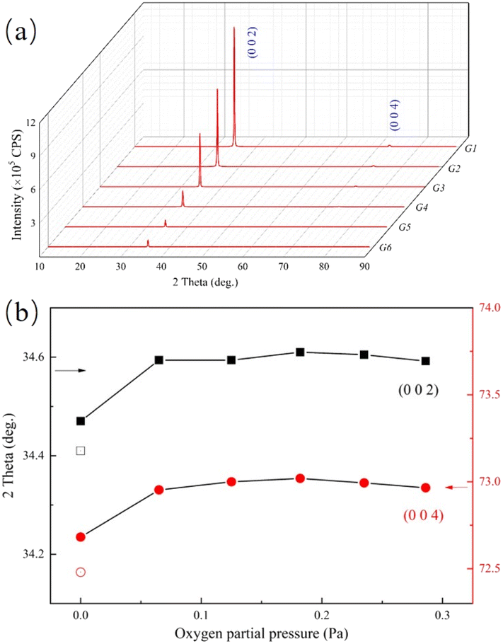 | ||
| Fig. 1 (a) XRD patterns of GZO; (b) the (0 0 2) and (0 0 4) peak positions of GZO at different oxygen partial pressures were indicated by solid squares and circles, respectively. The hollow square and circle corresponded to (002) and (004) peak positions of ZnO. | ||
However, the intensities of both (0 0 2) and (0 0 4) peaks decreased with increasing oxygen partial pressure due to a reduction in film thickness and the crystallinity degradation.
In Fig. 1(b) the value of parameter-c for G1 film was 5.12 Å, which was much smaller than that of pure ZnO (c = 5.21 Å). This suggested that the Ga ions effectively doped into the lattice of ZnO matrix because of the smaller ionic radius of Ga and the shorter bond with oxygen.
As the oxygen partial pressure increasing to 0.065 Pa in G2 film, the positions of (0 0 2) and (0 0 4) peaks sharply increased, and the value of parameter-c decreased to 5.10 Å. Although the oxygen partial pressure continued to increase, this value nearly remained unchanged.
The decrease in the value of parameter-c might be due to the increasing concentration of VZn because of its lowest formation energy in an oxygen-rich condition.6 The high concentration of VZn would induce a great Coulomb force of attraction among the ions around it, which may cause crystal distortion and contraction of crystal lattice.
The strain values of GZO films could be calculated by the eqn (1):11,12
 | (1) |
 | (2) |
| G1 | G2 | G3 | G4 | G5 | G6 | |
|---|---|---|---|---|---|---|
| ε (%) | −1.68 | −2.05 | −2.05 | −2.09 | −2.07 | −2.03 |
| σ (GPa) | 3.85 | 4.68 | 4.68 | 4.76 | 4.72 | 4.63 |
The impurity phases were analyzed by enlarging the XRD patterns. As shown in Fig. 2, there was no peak at the 2θ range of 30°–33° in G1, however, at the oxygen partial pressure of 0.065 Pa (G2), two new peaks appeared at 31.14° and 33.09°, which were indicated by arrows. The new peaks could be indexed to the orthorhombic structure of Ga2Zn6O9 (ICSD #173602).13 The intensity of each new peak was much lower than that of (0 0 2) peak from GZO, which indicated that the amount of the impurity was very small.
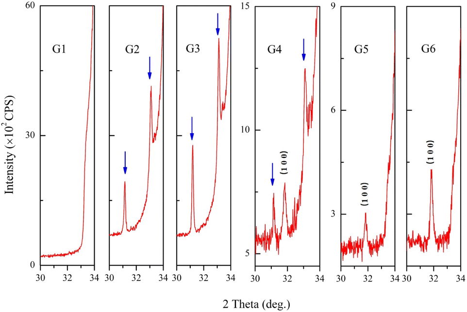 | ||
| Fig. 2 The XRD patterns of GZO at the range of 30°–34°. | ||
When the oxygen partial pressure increased to 0.182 Pa (G4), another new diffraction peak appeared at 31.16°, and it belonged to the (1 0 0) plane of GZO. The intensities of peaks belonging to Ga2Zn6O9 gradually diminished and disappeared when the oxygen partial pressure was 0.235 Pa (G5) or higher. The impurity of Ga2Zn6O9 appeared and disappeared during the increase of oxygen partial pressure, which implied that Ga ions might extract from the lattice of ZnO first and existed in the form of an amorphous state at higher oxygen partial pressure finally. This result suggested the effective doping of GaZn in lattice of ZnO matrix reduced. The parameter-c was almost unchanged in oxygen-rich conditions due to a small trace of impurity. Moreover, the diffraction peaks from Ga, Ga2O3 or ZnGa2O4 were not detected.
The defects and chemical states of GZO films were characterized by XPS. Ga-2p3/2 peaks were decomposed into two peaks at 1117.9 eV and 1118.6 eV, as shown in Fig. 3(a) and (b). The peak at 1117.9 eV was derived from the GaZn–O bonds, in which Ga atoms substituted for Zn atoms in ZnO matrix, while the peak at 1118.6 eV could be attributed to the Ga–O bonds duo to GaOx sub-oxides and oxides in intra-grain congregation or grain-boundary segregation.14–16 The intensity for the Ga-2p3/2 peak at 1117.9 eV decreased while it increased for the Ga-2p3/2 peak at 1183.6 eV. The results suggested that a number of Ga ions which replaced Zn in ZnO matrix were lost from the lattice of the matrix and might exist in the form of GaOx sub-oxides with the increasing oxygen partial pressure.
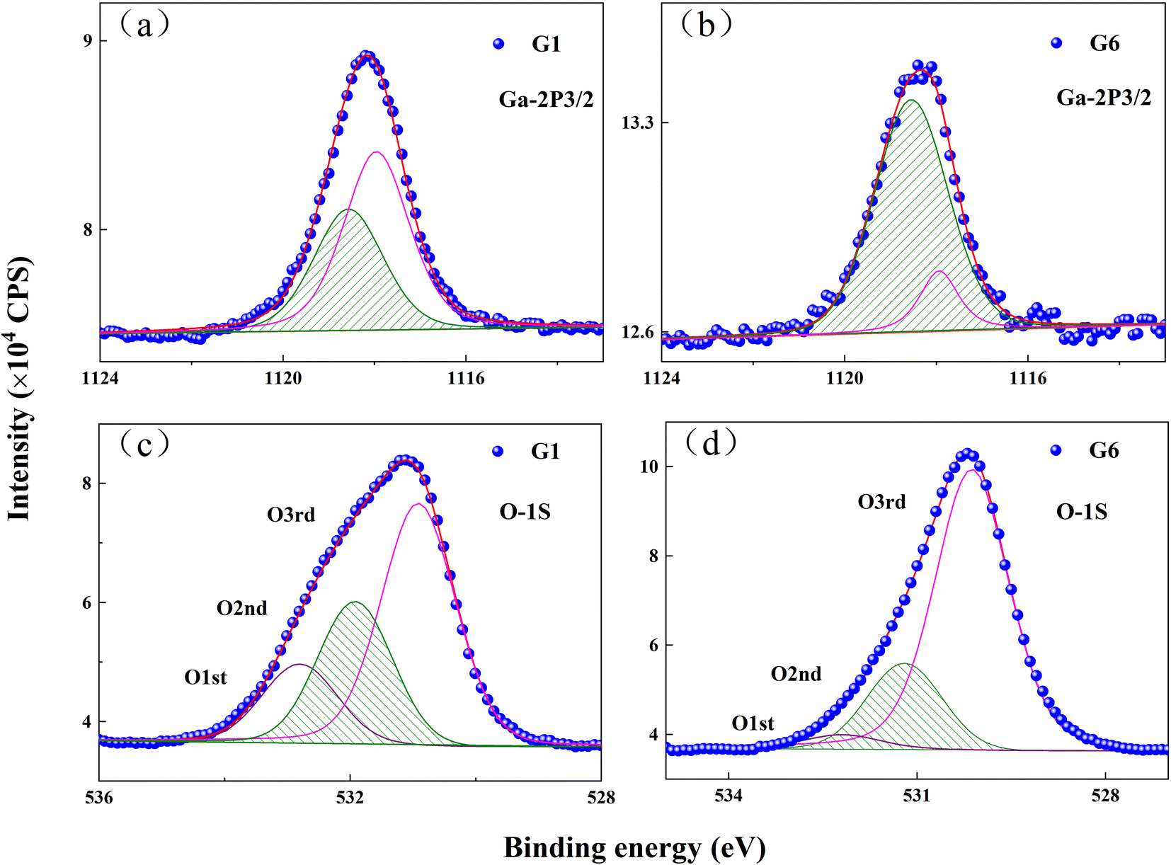 | ||
| Fig. 3 XPS spectra of Ga–2p3/2 peaks for: (a) G1 film; (b) G6 film, and O-1s peaks for: (c) G1 film; (d) G6 film. | ||
The asymmetric peak observed in the O-1s spectrum of G1 film could be fitted by three types of peaks, as shown in Fig. 3(c). The lowest binding energy peak of O-1s, centered at 530.6 eV, was marked as O3rd and derived from the bonds between O2− and metal ions (Zn2+ and Ga3+).17,18 The middle peak at 531.3 eV (O2nd) corresponded to oxygen vacancies in the G1 film.19,20 The highest binding energy at 532.2 eV was marked as O1st, which was related to oxygen near surface, such as O–H bonds.21,22 In comparison with the G1 film, the O1st, O2nd and O3rd peaks of G6 film were located at 530.2 eV, 531.3 eV and 532.3 eV in Fig. 3(d). The intensity of the O2nd peak was proportional to the concentration of oxygen vacancies.23 Peak intensity ratio of O2nd/Ototal was 26.7% for G1 film, but it decreased to 21% for G6 film, which indicated that the VO concentration in GZO film obviously decreased at the oxygen partial pressure.
The effect of oxygen partial pressure on the morphology of the GZO films was analyzed by using SEM. As shown in Fig. 4, the surface of the G1 film appeared compact and crack-free. In contrast, G2 film exhibited wide and deep boundaries, which became narrower in G3 film. The G4 film showed large grains with a tetrahedral shape, as indicated by arrows, and the number of these grains increased with increasing oxygen partial pressure.
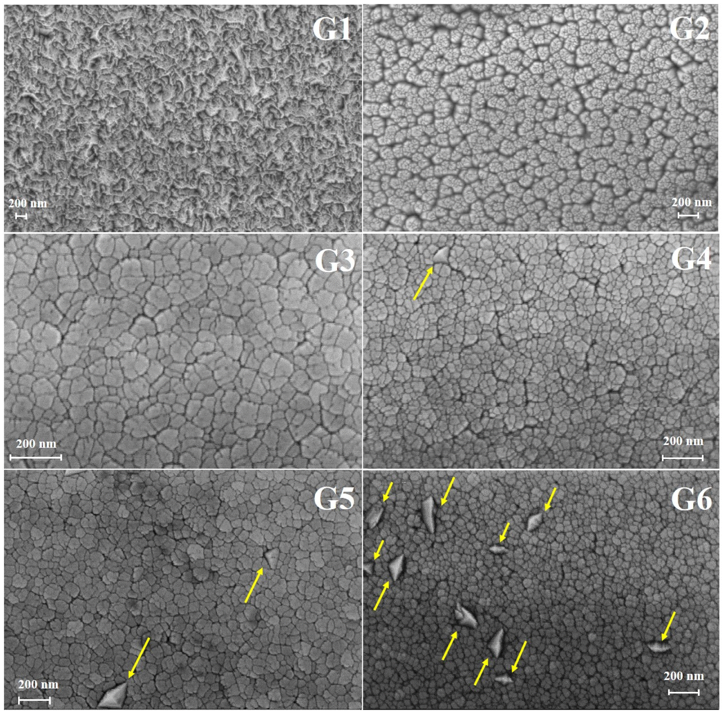 | ||
| Fig. 4 SEM images of GZO films deposited at various oxygen partial pressures. | ||
In general, the compact surface of G1 film turned into grains with a lot of boundaries in oxygen-rich conditions. The results suggested the nucleation and growth process during the formation of GZO films might be affected by oxygen, which reduced the island size in the coalescence stage.24,25 By comparison, it has been observed that the grain size of ZnO:Mg film decreased with the increasing oxygen partial pressure.26
Additionally, the tetrahedral grains could be caused by abnormal grain growth. In the oxygen-rich conditions, the mobility of boundary migration was limited, but some grain boundaries might have overcome the pinning effect and grown into larger sizes compared to other boundaries that were still pinned.27
3.1 Hall
The Hall effect measurement was conducted to analyze the electrical properties of the GZO films. In Fig. 5 the carrier concentration and resistivity were 8.6 × 1020 cm−3 and 4.5 × 10⁻⁴ Ω cm for the G1 film. In contrast, carrier concentration of the G2 film, which was deposited at an oxygen partial pressure of 0.065 Pa, decreased abruptly to 1.2 × 1018 cm−3 and the resistivity increased to 5.3 Ω cm. With increasing oxygen partial pressure, the carrier concentration gradually reduced (5.7 × 1017 cm−3, 1.5 × 1017 cm−3 and 1.4 × 1017 cm−3 for G3, G4 and G5 films), and the resistivity rose slowly (16.8 Ω cm, 24.9 Ω cm and 44.8 Ω cm for G3, G4 and G5 films). At the highest oxygen partial pressure of 0.286 Pa (G6), the concentration and resistivity reached values of 1.3 × 1017 cm−3 and 52.3 Ω cm, respectively. The same changes were also observed for mobility, which was as high as 16 cm2 V−1 S−1 for the G1 film, but it decreased to 0.9 cm2 V−1 S−1 for the G6 film. The decrease of mobility might mainly be caused by the increase of electron scattering induced by grain boundary.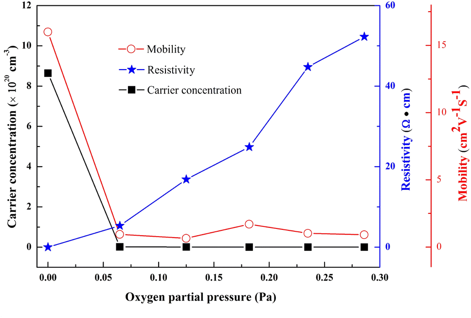 | ||
| Fig. 5 Resistivity, carrier concentration and Hall mobility of GZO films under various oxygen partial pressures. | ||
The high n-type carrier concentration (ntotal) for the G1 film was due to the high concentrations of GaZn and VO donor defects. The carrier concentration was reduced mainly due to the decrease of VO concentration and the increase of VZn concentration, which acted as compensating intrinsic defects.5
3.2 Transmittance
Optical transmittance spectra from 300 to 900 nm were analyzed by UV-vis spectrophotometer in Fig. 6. All of the spectra exhibited sharp absorption edges, and the average optical transmittance of each GZO film deposited under oxygen partial pressure was more than 90% for the wavelength above 450 nm. The optical transmittance of G1 film gradually decreased as the wavelength increased in the near-infrared (NIR) region due to absorption by the free carrier plasm resonance frequency.28 The absorption edge of the G1 spectrum shifted to longer wavelength in oxygen-rich conditions.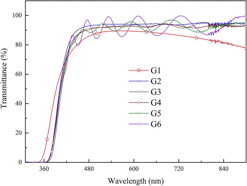 | ||
| Fig. 6 Transmission spectra of GZO films in the region of 300–900 nm. | ||
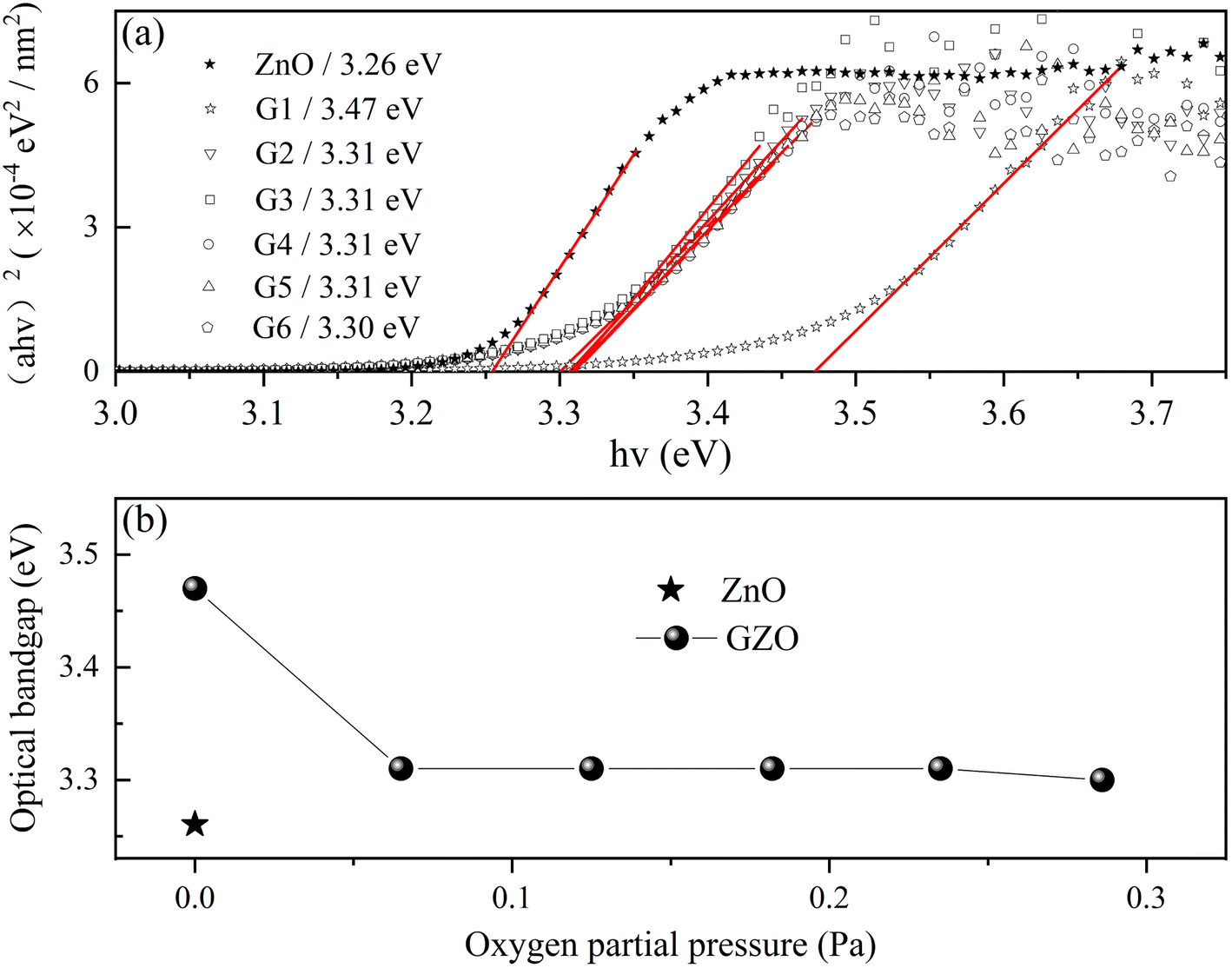
Fig. 7(a) and (b) showed the variation of the optical bandgap with increasing oxygen partial pressures. The bandgap of the G1 film was 3.47 eV and decreased rapidly to 3.31 eV under an oxygen partial pressure of 0.065 Pa (G2). The optical bandgaps then remained almost constant at 3.31 eV with increasing oxygen partial pressure, which were larger than that of the pure ZnO film (3.26 eV).
 | ||
| Fig. 7 The (a) and (b) showed the optical bandgap of GZO (ball) varied with the O2 partial pressure and the value of ZnO was indicated by the symbol of star. | ||
The optical bandgap of the G1 film was the largest due to the Burstein–Moss (B–M) effect, which described the blue-shift of the optical bandgap energy. The relationship between the broadening of the optical band gap (ΔEg) and carrier concentration (n) could be expressed by eqn (3):3,29
 | (3) |
The UPS spectra for G1, G6, and ZnO films were shown in Fig. 8(a)–(c), respectively. The error tolerances in our analyses were ±0.15 eV. The VBM was determined by the cross point at the linear extrapolation of the edge of UPS and the baseline (X-axis). The band structures of G1, G6 and ZnO were shown by Fig. 8(d)–(f), respectively, by combining them with the optical band gap. The electron affinity of G1 was 3.57 eV, while it was 3.54 eV for G6. The result suggested that oxygen partial pressure had almost no effect on the electron affinity, which was a key parameter in band alignment of device consisting with multilayer films. For comparison, the electron affinity of ZnO was as high as 4.49 eV, which was much larger than G6, although both ZnO and G6 were insulated. The experimental results showed that the electron affinity of ZnO could be effectively tuned by doping Ga, but electron affinity of GZO had almost not been affected by oxygen partial pressure.
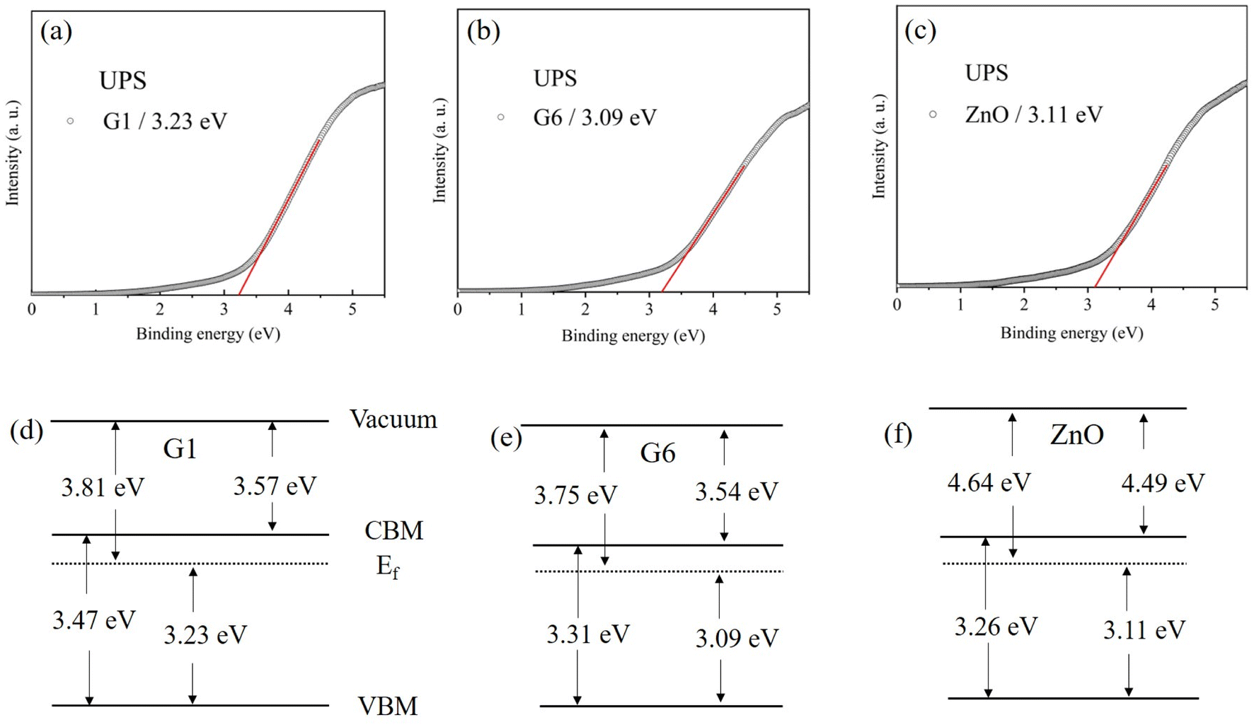 | ||
| Fig. 8 (a)–(c) were UPS spectra which correspond to G1, G6 and ZnO films. (d)–(f) Were sketches of band structures which correspond to G1, G6 and ZnO films. | ||
4. Conclusions
In summary, the GZO films were deposited by using RF sputtering method. The effects of oxygen partial pressure on structure and performance of GZO films have been investigated. The value of parameter-c decreased at an oxygen partial pressure of 0.065 Pa and then almost remained unchanged until the pressure increased to 0.286 Pa. It was the first time that the impurity of Ga2Zn6O9 appeared first and disappeared finally with the increase in oxygen partial pressure.The opto-electrical properties of GZO films deposited at different oxygen partial pressures were measured. The resistivity increased from 4.5 × 10⁻⁴ Ω cm to 52.3 Ω cm when the oxygen partial pressure increased from 0 to 0.286 Pa, mainly due to the decrease of VO concentration and the increase of VZn concentration, which acted as compensating intrinsic defects. Meanwhile, the optical bandgap of GZO film decreased with the increase in oxygen partial pressure from 3.47 eV to about 3.30 eV. The results showed that the conductivity and optical bandgap of GZO film were easily affected by oxygen partial pressure. Additionally, the electron affinities were 3.57 eV and 3.54 eV for G1 and G6, respectively, and it was proved that the oxygen partial pressure had almost no effect on the electron affinity of GZO film in oxygen-rich condition. For comparison, the electron affinity of ZnO film was 4.49 eV, which suggested that Ga played an important role in tuning electron affinity of ZnO film.
Conflicts of interest
There are no conflicts to declare.Acknowledgements
This work is supported by Lujiaxi International Team Project of CAS (No: GJTD-2018-05).References
- D. O. Demchenko, B. Earles, H. Y. Liu, V. Avrutin, N. Izyumskaya, U. Ozgur and H. Morkoc, Impurity complexes and conductivity of Ga-doped ZnO, Phys. Rev. B: Condens. Matter Mater. Phys., 2011, 84, 075201, DOI:10.1103/PhysRevB.84.075201.
- B. X. Lin, Z. X. Fu and Y. B. Jia, Green luminescent center in undoped zinc oxide films deposited on silicon substrates, Appl. Phys. Lett., 2001, 79, 943–945, DOI:10.1063/1.3703515.
- G. C. Park, S. M. Hwang, J. H. Lim and J. Joo, Growth behavior and electrical performance of Ga-doped ZnO nanorod/p-Si heterojunction diodes prepared using a hydrothermal method, Nanoscale, 2014, 6, 1840–1847, 10.1039/c3nr04957d.
- T. Nam, C. W. Lee, H. J. Kim and H. Kim, Growth characteristics and properties of Ga-doped ZnO (GZO) thin films grown by thermal and plasma-enhanced atomic layer deposition, Appl. Surf. Sci., 2014, 295, 260–263, DOI:10.1016/j.apsusc.2014.01.027.
- C. S. Lee, C. H. Jeon, B. T. Lee and S. H. Jeong, Abrupt conversion of the conductivity and band-gap in the sputter grown Ga-doped ZnO films by a change in growth ambient: effects of oxygen partial pressure, J. Alloys Compd., 2018, 742, 977–985, DOI:10.1016/j.jallcom.2018.01.351.
- M. H. Lee, Y. C. Peng and H. C. Wu, Effects of intrinsic defects on electronic structure and optical properties of Ga-doped ZnO, J. Alloys Compd., 2014, 616, 122–127, DOI:10.1016/j.jallcom.2014.07.098.
- D. C. Look, K. D. Leedy, L. Vines, B. G. Svensson, A. Zubiaga, F. Tuomisto, D. R. Doutt and L. J. Brillson, Self-compensation in semiconductors: the Zn vacancy in Ga-doped ZnO, Phys. Rev. B, 2011, 84, 115202, DOI:10.1103/PhysRevB.84.115202.
- X. Q. Li, H. K. Zhang, X. B. Lu, Z. Q. Fang, R. H. Yao, Y. P. Wang, H. Tao, H. F. Liang, H. L. Ning and J. B. Peng, Effect of oxygen pressure on GZO film as active layer of the TFT fabricated at room temperature, Superlattices Microstruct., 2020, 137, 106317, DOI:10.1016/j.spmi.2019.106317.
- W. S. Noha, J. A. Lee, J. H. Lee, Y. W. Heo and J. J. Kim, Effect of oxygen pressure on the p-type conductivity of Ga, P co-doped ZnO thin film grown by pulsed laser deposition, Ceram. Int., 2016, 42, 4136–4142, DOI:10.1016/j.ceramint.2015.11.086.
- Y. Q. Wang, W. Tang and L. Zhang, Crystalline size effects on texture coefficient, electrical and optical properties of sputter-deposited Ga-doped ZnO thin films, J. Mater. Sci. Technol., 2015, 31, 175–181, DOI:10.1016/j.jmst.2014.11.009.
- L. B. Freund and E. Chason, Model for stress generated upon contact of neighboring islands on the surface of a substrate, J. Appl. Phys., 2001, 89, 4866–4873, DOI:10.1063/1.1359437.
- L. Li, L. Fang, X. M. Chen, J. Liu, F. F. Yang, Q. J. Li, G. B. Liu and S. J. Feng, Influence of oxygen argon ratio on the structural, electrical, optical and thermoelectrical properties of Al-doped ZnO thin films, Phys. E, 2008, 41, 169–174, DOI:10.1016/j.physe.2008.07.001.
- Y. Michiue, N. Kimizuka and Y. Kanke, Structure of Ga2O3(ZnO)6: a member of the homologous series Ga2O3(ZnO)m, Acta Crystallogr., Sect. B: Struct. Sci., 2008, 64, 521–526, DOI:10.1107/S0108768108021125.
- H. Jung, D. Kim and H. Kim, The electrical properties of low pressure chemical vapor deposition Ga doped ZnO thin films depending on chemical bonding configuration, Appl. Surf. Sci., 2014, 297, 125–129 CrossRef CAS.
- J. G. Lu, Z. Z. Ye, Y. J. Zeng, L. P. Zhu, L. Wang, J. Yuan, B. H. Zhao and Q. L. Liang, Structural, optical, and electrical properties of (Zn, Al)O films over a wide range of compositions, J. Appl. Phys., 2006, 100, 073714 CrossRef.
- C. L. Hinkle, M. Milojevic, B. Brennan, A. M. Sonnet, F. S. Aguirre-Tostado, G. J. Hughes, E. M. Vogel and R. M. Wallace, Detection of Ga suboxides and their impact on III–V passivation and Fermi-level pinning, Appl. Phys. Lett., 2009, 94, 162101 CrossRef.
- M. C. Biesinger, L. W. M. Lau, A. R. Gerson and R. S. C. Smart, Resolving surface chemical states in XPS analysis of first row transition metals, oxides and hydroxides: Sc, Ti, V, Cu and Zn, Appl. Surf. Sci., 2010, 257, 887–898, DOI:10.1016/j.apsusc.2010.07.086.
- S. C. Ghosh, M. C. Biesinger, R. R. Lapierre and P. Kruse, X-ray photoelectron spectroscopic study of the formation of catalytic gold nanoparticles on ultraviolet–ozone oxidized GaAs (100) GaAs (100) substrates, J. Appl. Phys., 2007, 101, 114322, DOI:10.1063/1.2743729.
- Y. K. Liao, S. J. Jiao, S. F. Li, J. Z. Wang, D. B. Wang, S. Y. Gao, Q. J. Yu and H. T. Li, Effect of deposition pressure on the structural and optical properties of Ga2O3 films obtained by thermal post-crystallization, CrystEngComm, 2018, 20, 133–139, 10.1039/C7CE01567D.
- G. D. Wu, G. Q. Zhao, J. H. Sun, X. Z. Cao, Y. F. He, J. T. Feng and D. Q. Li, The effect of oxygen vacancies in ZnO at an Au/ZnO interface on its catalytic selective oxidation of glycerol, J. Catal., 2019, 377, 271–282, DOI:10.1016/j.jcat.2019.06.030.
- C. Y. Tsay, K. S. Fan and C. M. Lei, Synthesis and characterization of sol–gel derived gallium-doped zinc oxide thin films, J. Alloys Compd., 2012, 512, 216–222, DOI:10.1016/j.jallcom.2011.09.066.
- M. Futsuhara, K. Yoshioka and O. Takai, Structural, electrical and optical properties of zinc nitride thin films prepared by reactive rf magnetron sputtering, Thin Solid Films, 1998, 322, 274–281, DOI:10.1016/S0040-6090(97)00910-3.
- B. Salameh, A. M. Alsmadi and M. Shatnawi, Effects of Co concentration and annealing on the magnetic properties of Co-doped ZnO films: role of oxygen vacancies on the ferromagnetic ordering, J. Alloys Compd., 2020, 835, 155287, DOI:10.1016/j.jallcom.2020.155287.
- R. Saha, N. R. Saha, A. Karmakar, G. K. Dalapati and S. Chattopadhyay, Generation of oxygen interstitials with excess in situ Ga doping in chemical bath deposition process for the growth of p-type ZnO nanowires, J. Mater. Sci.: Mater. Electron., 2019, 30, 8796–8804, DOI:10.1007/s10854-019-01204-4.
- L. B. Freund and E. Chason, Model for stress generated upon contact of neighboring islands on the surface of a substrate, J. Appl. Phys., 2001, 89, 4866–4873, DOI:10.1063/1.1359437.
- X. X. Suo, S. J. Zhao, Y. J. Ran, H. N. Liu, Z. T. Jiang, Y. L. Li and Z. Wang, Effects of oxygen/argon pressure ratio on the structural and optical properties of Mn-doped ZnO thin films prepared by magnetron pulsed co-sputtering, Surf. Coat. Technol., 2019, 357, 978–983, DOI:10.1016/j.surfcoat.2018.10.084.
- I. Basu, K. G. Pradeep, C. Miessen, L. A. Barrales-Mora and T. Al-Samman, The role of atomic scale segregation in designing highly ductile magnesium alloys, Acta Mater., 2016, 116, 77–94, DOI:10.1016/j.actamat.2016.06.024.
- C. Y. Tsai, C. Y. Tsai, C. H. Chen, T. L. Sung, T. Y. Wu and F. P. Shih, Theoretical model for intravalley and intervalley free-carrier absorption in semiconductor lasers: Beyond the classical Drude model, IEEE J. Quantum Electron., 1998, 34, 552–559, DOI:10.1109/3.661466.
- J. Liu, W. Zhang, D. Song, Q. Ma, L. Zhang, H. Zhang, X. B. Ma and H. Y. Song, Comparative study of the sintering process and thin film sputtering of AZO, GZO and AGZO ceramics targets, Ceram. Int., 2014, 40, 12905–12915, DOI:10.1016/j.ceramint.2014.04.150.
| This journal is © The Royal Society of Chemistry 2023 |