
 Open Access Article
 This Open Access Article is licensed under a Creative Commons Attribution-Non Commercial 3.0 Unported Licence
Electronic and optical properties of thiogermanate AgGaGeS4: theory and experiment
Tuan V. Vu *ab,
Vo D. Datab,
A. A. Lavrentyevc,
B. V. Gabreliand,
Nguyen N. Hieuef,
G. L. Myronchukgh and
O. Y. Khyzhun*gh
*ab,
Vo D. Datab,
A. A. Lavrentyevc,
B. V. Gabreliand,
Nguyen N. Hieuef,
G. L. Myronchukgh and
O. Y. Khyzhun*gh
aLaboratory for Computational Physics, Institute for Computational Science and Artificial Intelligence, Van Lang University, Ho Chi Minh City, Vietnam. E-mail: tuan.vu@vlu.edu.vn
bFaculty of Mechanical – Electrical and Computer Engineering, Van Lang University, Ho Chi Minh City, Vietnam
cDepartment of Electrical Engineering and Electronics, Don State Technical University, 1 Gagarin Square, 344010 Rostov-on-Don, Russian Federation
dDepartment of Computational Technique and Automated System Software, Don State Technical University, 1 Gagarin Square, 344010 Rostov-on-Don, Russian Federation
eInstitute of Research and Development, Duy Tan University, Da Nang 550000, Vietnam
fFaculty of Natural Sciences, Duy Tan University, Da Nang 550000, Vietnam
gDepartment of Experimental Physics and Information-Measuring Technology, Lesya Ukrainka Volyn National University, 13 Voli Avenue, 43025 Lutsk, Ukraine
hFrantsevych Institute for Problems of Materials Science, National Academy of Sciences of Ukraine, 3 Krzhyzhanivsky Street, 03142 Kyiv, Ukraine. E-mail: khyzhun@ipms.kiev.ua
First published on 4th January 2023
Abstract
The electronic and optical properties of an AgGaGeS4 crystal were studied by first-principles calculations, where the full-potential augmented plane-wave plus local orbital (APW+lo) method was used together with exchange–correlation pseudopotential described by PBE, PBE+U, and TB-mBJ+U approaches. To verify the correctness of the present theoretical calculations, we have measured for the AgGaGeS4 crystal the XPS valence-band spectrum and the X-ray emission bands representing the energy distribution of the electronic states with the biggest contributions in the valence-band region and compared them on a general energy scale with the theoretical results. Such a comparison indicates that, the calculations within the TB-mBJ+U approach reproduce the electron-band structure peculiarities (density of states – DOS) of the AgGaGeS4 crystal which are in fairly good agreement with the experimental data based on measurements of XPS and appropriate X-ray emission spectra. In particular, the DOS of the AgGaGeS4 crystal is characterized by the existence of well-separated peaks/features in the vicinity of −18.6 eV (Ga-d states) and around −12.5 eV and −7.5 eV, which are mainly composed by hybridized Ge(Ga)-s/p and S-p state. We gained good agreement between the experimental and theoretical data with respect to the main peculiarities of the energy distribution of the electronic S 3p, Ag 4d, Ga 4p and Ge 4p states, the main contributors to the valence band of AgGaGeS4. The bottom of the conduction band is mostly donated by unoccupied Ge-s states, with smaller contributions of unoccupied Ga-s, Ag-s and S-p states, too. The AgGaGeS4 crystal is almost transparent for visible light, but it strongly absorbs ultra-violet light where the significant polarization also occurs.
1 Introduction
Laser sources working in the UV, near-infrared, and mid-infrared ranges have shown their important role in many practical applications such as atmospheric and solar guidance, free-space communication, detectors, and others.1–7 Therefore, many nonlinear optical crystals have intensively been studied and developed to produce laser sources of these ranges.3,8–12 Among these materials, special attention has been paid to those which can effectively convert the 1.060–1.064 μm emission from commercially available laser medium sources such as Nd:YAG, Nd:Cr:YAG, Nd:YLF, Nd:YVO4, and Nd:YCO.13–16 However, only a few of the explored nonlinear optical materials, namely AgGaS2, AgGaSe2, and ZnGeP2,17–21 are suitable for practical uses. At the same time, practical applications of these NLO crystals are also limited when pumping within the 1–9 μm range due to the opaqueness to wavelengths less than 2 μm and the multi-phonon absorption at wavelengths more than 9 μm. Laser damage threshold causes another practical restriction of these crystals because the anisotropic thermal expansion lowers their resistance to thermal shock.19,21–24With many advantages over the drawbacks of the aforementioned compounds, a thiogermanate AgGaGeS4 crystal is currently considered among best NLO materials. The AgGaGeS4 crystal possesses a wider transparency range (0.5–11.5 μm)25 in comparison with ZnGeP2. Its residual absorption around 1.064 μm wavelengths is as low as 0.05 cm−1 making the titled crystal to be suitable for Nd:YAG laser pumping.26 The laser damage threshold of AgGaGeS4 was revealed to be 203 MW cm−2 at 2.05 μm,27 and 230 MW cm−2 at 9.55 μm,28 allowing applications of operating conditions at higher current powers than AgGaS2 or AgGaSe2 crystals allow.27,28 Moreover, AgGaGeS4 crystal reveals a wide range of phase-matching schemes, allowing the crystal to be effectively used for various frequency conversions.29,30 Finally, the growth/synthesis conditions were successfully explored aiming to obtain high-pure and large-size AgGaGeS4 crystals (centimeter dimensions) that can be effectively used to convert over wide range of wavelengths including 1.064 μm, 4 μm, and 11 μm.
Most of studies of AgGaGeS4 crystals depend essentially on experimental conditions and quality of the crystals. During the growth of AgGaGeS4 crystals, many defects may occur forming additional electronic states in the band gap, making its value varying from 2.25 till 2.80 eV.31,32 In particular, vacancies on special crystallography sites have been established to form during annealing AgGaGeS4 crystals and their presence affects the band gap value being within the energy range of 2.787–2.805 eV in such a case.25 Moreover, the band gap of AgGaGeS4 was experimentally discovered to be inversely proportional to temperature value,33 and at temperatures lower than 100 K, the band gap of AgGaGeS4 is bigger than 3 eV. It is well-known that the electronic structure plays a crucial role in determining the optical properties of semiconductors. For the case of AgGaGeS4 crystal considering a promising laser convertor, the value of the band gap is very important as it determines the transparency of semiconducting materials. In this study, a detailed knowledge about the electronic structure of the AgGaGeS4 crystal as well as its optical properties is provided based on first-principles calculations. It is worth mentioning that, to the best of our knowledge, the electronic structure of AgGaGeS4 has not been studied theoretically yet. Furthermore, the theoretical densities of states of AgGaGeS4 are verified in the present work by using measurements of experimental XPS and X-ray emission spectra.
2 Calculation method
The unit-cell of the AgGaGeS4 crystal was constructed using its space group Fdd2 and the lattice parameters a = 12.019 Å, b = 22.924 Å, c = 6.8837 Å as established in ref. 34 in which each Ga or Ge atom belongs to a tetrahedron formed by S atoms, while Ag atoms occupy the space between these tetrahedra as presented in Fig. 1. For structural optimization as well as electronic properties calculations, a 1 × 1 × 1 supercell is used, and the Brillouin zone is sampled with a 1000-k-point mesh to satisfy requirements of density functional theory (DFT) methods as implemented in the WIEN2k package, where the Kohn–Sham equations are solved by the APW+lo method.35 In the APW+lo method, for the case of the AgGaGeS4 crystal, the unit cell is partitioned into atomic spheres for Ag, Ga, Ge, and S atoms with their radii RMT of 2.5, 2.2, 2.26, 1.91 a. u., respectively, where the basis functions are expressed as the sum of atomic partial waves to the maximum angular momentum lmax = 10, and the electron density ρ is expanded as Fourier series up to Gmax = 14 a. u.−1. Meanwhile, in the interstitial space of the unit cell, the plane waves are summed up to lmax = 4, and ρ is presented as the sum of the product of lattice harmonics and radial functions. Because thiogermanate AgGaGeS4 is a semiconductor consisting of atoms involving d orbitals, either Perdew–Burke–Ernzerhof generalized gradient approximation (PBE)36 or Tran and Blaha modified Becke–Johnson (TB-mBJ) potential37 are known to produce reasonable results being used for the exchange–correlation potential in such a case and the Hubbard parameter U38,39 was also included to treat the Coulomb interactions between local orbitals.40,41 The parameter RminMT × kmax = 8.0 is used as convergence criterion of the scf-calculations, while the iterations are suggested to reach the convergence when the difference in charge density for two subsequent iterations is less than 10−4 Ry. After reaching the convergence, an equilibrium structure of AgGaGeS4 is achieved together with its wave functions |knσ〉 at wave vector k and spin σ, and the corresponding eigenvalues of energy Ekn. This information can be used to calculate the imaginary part ε2(ω) of the dielectric function ε(ω) = ε1(ω) + iε2(ω) at the angular frequency ω of the electromagnetic radiation by applying the momentum operator p on the wave function |knσ〉 as follows:42
 | (1) |
 | ||
| Fig. 1 (a) Positions of the atoms and (b) stacking the [GaS4] and [GeS4] tetrahedra in the AgGaGeS4 unit cell that is outlined, for clarity. | ||
3 Experimental
For the present X-ray spectroscopy measurements, we use the AgGaGeS4 crystal synthesized by the two-zone Bridgman method in ref. 34. In the above article, it was proved that the crystal under consideration is of high optical quality and without any additional phase admixtures. Therefore, in the present work we report on measurements of X-ray emission Ag Lβ2,15 (NIV,V → LIII transition) and Ga(Ge) Kβ2 (NII,III → KI transition) bands, which represent the energy distribution of the valence Ag d and Ga(Ge) p states, respectively. The X-ray emission Ag Lβ2,15 and Ga(Ge) Kβ2 bands were derived using DRS-2M spectrographs equipped with X-ray BKhV-7 tubes (gold anodes) using quartz crystals with the (10![[1 with combining macron]](https://www.rsc.org/images/entities/char_0031_0304.gif) 0) and (13
0) and (13![[4 with combining macron]](https://www.rsc.org/images/entities/char_0034_0304.gif) 0) reflecting planes, respectively. The both crystals were focused by the Rowland circle geometry following Johann's technique.45 The details of the present X-ray emission measurements are similar to those described in details in ref. 46 and 47 in the case of the Ag Lβ2,15 band and the Ga(Ge) Kβ2 bands, respectively. The XPS valence-band spectrum of the AgGaGeS4 crystal was measured using the UHV-analysis system following the technique;34 however, to gain better resolution, in the present work we employ a Mg Kα source (E = 1253.6 eV) and the spectrum was recorded at constant pass energy of 20 eV. The XES S Kβ1,3 band was measured as reported in ref. 34.
0) reflecting planes, respectively. The both crystals were focused by the Rowland circle geometry following Johann's technique.45 The details of the present X-ray emission measurements are similar to those described in details in ref. 46 and 47 in the case of the Ag Lβ2,15 band and the Ga(Ge) Kβ2 bands, respectively. The XPS valence-band spectrum of the AgGaGeS4 crystal was measured using the UHV-analysis system following the technique;34 however, to gain better resolution, in the present work we employ a Mg Kα source (E = 1253.6 eV) and the spectrum was recorded at constant pass energy of 20 eV. The XES S Kβ1,3 band was measured as reported in ref. 34.
4 Results and discussion
4.1 Calculated electronic structure and XPS and XES data for the AgGaGeS4 crystal
The major distinction between PBE, PBE+U, and TB-mBJ+U methods is that, how these methods describe exchange–correlation potential, which affects the theoretical electronic structure of a solid, in particular AgGaGeS4. In order to determine the best method for evaluating the electronic band structure of the AgGaGeS4 crystal, both theoretical total density of state and the experimental XPS valence-band spectrum are shown in Fig. 2, where the Fermi level has been shifted to 0 eV corresponding to the top of the highest occupied valence band in the compound under consideration. It is well known that, the XPS technique induces a higher energy position of the Fermi level than the theoretical valence highest bands48 (in our case, zero of the energy scale of the experimental XPS spectrum corresponds to the Fermi level of the energy analyzer used in the UHV-analysis system, in fact, a PHOIBOS 150 analyzer). Therefore, presented in Fig. 2 the XPS valence band spectrum measured for the AgGaGeS4 crystal was shifted by 0.9 eV toward the direction of the EF position to gain correspondence between most prominent peaks/peculiarities detected for the experimental and theoretical results as recommended to do in the case of semiconducting materials.47 | ||
| Fig. 2 Experimental electronic structure as determined in the present work by measurements of the XPS valence band spectrum versus theoretical total density of states revealed by DFT calculations employing the PBE, PBE+U and TB-mBJ+U approaches for AgGaGeS4. | ||
Fig. 2 shows a noticeable variation in the energy band gaps of the AgGaGeS4 crystal as it is calculated by the PBE, PBE+U, and TB-mBJ+U methods, which are found to be equal to 1.575 eV, 2.012 eV, and 3.414 eV, respectively (note that, the values of UGa = 0.65 Ry and UAg = 0.5 Ry are used in the present DFT calculations). It is worth mentioning that, we treated different U parameters for finding the best correspondence of the shapes of theoretical DOS curves with the experimental XPS spectrum, energy positions of their most prominent fine-structure peculiarities and Eg values. In the present work we present data only for the case of the best agreement between the theoretical and experimental data. Available experimental data reveal the band gap of about 2.84 eV for AgGaGeS4 at room temperature.25,31,49 Meanwhile, Davydyuk et al.33 have shown experimental data where the band gap of the AgGaGeS4 is from 2.84 eV to above 3 eV. Therefore, in our opinion, the TB-mBJ+U method, which features the energy band gap of 3.414 eV, looks to be the most suitable for calculating the electronic properties of the AgGaGeS4 crystal. By Pauli principles, electrons with the same spin avoid each other causing the exchange effect; meanwhile electrons with opposite spin interact with each other due to the correlation effect. Both effects are not correctly introduced in the PBE method providing the interaction of an electron with itself. Due to the ground-state nature of the DFT approach, the valence band values are overestimated under such circumstances. This overestimation does not happen to the unoccupied conduction bands; therefore, the energy band gap occurring between the valence and conduction bands is narrowed. As it is shown in Fig. 2, the band gap revealed by the PBE method is by about 0.5 eV smaller than that derived by employing the PBE+U method. The Hubbard parameter U was introduced to the PBE+U method in the present DFT calculations to provide some correction to the correlation effect of the core electrons. This correlation correction effect, as it is evidenced from Fig. 2, improves the theoretical energy band gap value of the AgGaGeS4 crystal and provides better valence band structure regarding the shape of the experimental XPS valence-band spectrum. The main peak occurring at around −3 eV in the PBE-derived spectrum shifts down to −4 eV in the PBE+U-like spectrum. In the latter case, the main valence band peak coincides well with the energy position of the peak B of the XPS curve. One of the most important improvements in the present DFT calculations brought by the U correction technique is the rearrangement of the electron energy levels. The PBE+U method recognizes more electrons for the electronic states positioned near −3 eV, and features another high intensity peak to be located near −18.1 eV instead of −14.9 eV as derived by the PBE method. These electronic peculiarities are in good agreement with the XPS data. It is worth mentioning that, the exchange correction is introduced in the TB-mBJ approach by a short-range potential model.37 As can be seen from Fig. 2, when employing the U correction technique using TB-mBJ potential37 (the TB-mBJ+U method), we observe better correspondence of the theoretical total DOS curve to the experimental electronic structure of the AgGaGeS4 crystal; in such a case, the main peak near −18.6 eV is located exactly around the energy position of the peak E detected in the XPS valence-band spectrum and with an expected relative intensity.
Curves of partial DOS of AgGaGeS4 are presented in Fig. 3. The highest peak E of the XPS spectrum corresponds to the energy level around −18.6 eV in the theoretical DOS curve, where the electrons originating from Ga-d orbitals form the densest electronic state sub-band. The Ge(Ga)-s/p and S–s orbitals mainly donate into broader energy regions, however less dense sub-bands, ranging from −14.3 to −11 eV, and −8 to −7 eV. These bands correspond to the D and C peaks in the XPS spectrum, respectively. In the highest energy levels of the valence band of AgGaGeS4 ranging from −6.1 to 0 eV, the Ag-d orbitals donate major parts to the peak B at −4 eV. As can be seen from Fig. 3, Ga-s states bring the principal contributions to the bottom of the valence band, Ga-p and S-p states produce the formation of the near-Fermi feature A of the XPS spectrum, while S-p states dominate at the top of the valence band of the quaternary sulfide under consideration. In addition to the above-mentioned contributors, Fig. 3 presents that Ge-p states also substantially contribute to the peak B of the XPS valence band spectrum of AgGaGeS4.
 | ||
| Fig. 3 Experimental electronic structure (XPS valence-band spectrum, XES S Kβ1,3, Ag Lβ2,15, Ga Kβ2 and Ge Kβ2 bands) versus total DOS and its main constituent orbitals calculated by TB-mBJ+U for AgGaGeS4 crystal. | ||
To verify the above predictions made on the basis of the present DFT calculations, we have performed XES measurements of the appropriate bands giving information on the partial densities of states for atoms composing AgGaGeS4. Our estimations employing the XPS technique bring the following atomic percentage of the constituting chemical elements in the AgGaGeS4 crystal under study: 14.9 at% Ag, 12.2 at% Ga, 14.6 at% Ge, 58.3 at% S. The nominal atomic percentage in the ideal AgGaGeS4 crystal should be as follows: 14.3 at% Ag, 14.3 at% Ga, 14.3 at% Ge, 57.1 at% S. Our XPS data indicate that the composition of the constituting chemical elements in the AgGaGeS4 crystal used for the present experiments is close to the ideal composition for all the atoms except of Ga. In particular, literature data indicates50 that some deficit of Ga in the AgGaGeS4 crystals looks to be a problem for such kinds of compounds. In particular, partial lack of Ga atoms in comparison to the expected theoretically atomic ratios was detected previously for a series of AgGaGeS4·nGeS2 crystals possessing the crystal structure belonging to the SG Fdd2, with n equal to 0, 2, 3, and 4. We believe that this small lack of Ga in the crystal being investigated does not influence the present experimental results. In the present experiments we do not detect XPS or XES spectral peculiarities associated with vacancy formation. It should be noted that our XPS measurements of the XPS core-level Ga 2p3/2, Ag 3d5/2, and Ge 3d spectra in the AgGaGeS4 crystal34 indicate that their binding energies are equal to 1117.35(±0.05), 367.45(±0.05), and 30.86(±0.05) eV, respectively, being in excellent agreement with the XPS data by Huang et al.51 for AgGaGenS2(n+1) (n = 2, 3, 4, and 5) crystals. For the latter crystals, the XPS measurements51 give the binding energies of 1117.35–1117.03 eV, 367.45–367.38 eV, and 30.88–30.87 eV for the XPS core-level Ga 2p3/2, Ag 3d5/2, and Ge 3d spectra, respectively. Interestingly, the authors51 have detected some tendency of decreasing binding energies for the XPS core-level Ga 2p3/2 and Ag 3d5/2 spectra in the AgGaGenS2(n+1) crystals with increasing the n value, while the binding energy of the Ge 3d spectra remains unchanged in such a case.
It is well-known that the X-ray emission S Kβ1,3, Ag Lβ2,15, Ga Kβ2 and Ge Kβ2 bands plotted in Fig. 3 represent the energy distributions of the valence electronic S-p, Ag-d, Ga-p and Ge-p states, respectively.45,52,53 As shown in Fig. 3, the maximum position of the XES S Kβ1,3 band is located around the peculiarity A of the XPS spectrum indicating that the main contributions of S 3p states are expected to be positioned in the upper part of the AgGaGeS4 valence band, with essential contributions of these electronic states throughout the whole band region ranging from −6.1 to 0 eV being in excellent predictions of the present DFT calculations. Furthermore, the maxima of the XES Ag Lβ2,15 and Ge Kβ2 bands are detected around the main maximum B of the XPS valence-band spectrum of the AgGaGeS4 crystal, while the maximum of the Ga Kβ2 band is detected in the vicinity of the shoulder A of the XPS spectrum. These experimental data indicate that the valence Ag-d, and Ge-p states contribute mainly in the energy region in the vicinity of the maximum B of the XPS spectrum, while Ga-p states around the peculiarity A, again supporting the present DFT band-structure calculations of the AgGaGeS4 compound. Therefore, we gain good agreement between the experimental and theoretical data with respect to the main peculiarities of the energy distribution of the electronic S 3p, Ag 4d, Ga 4p and Ge 4p states, the main contributors to the valence band of AgGaGeS4. Some peculiar hybridization of the mentioned electronic states is observed in the AgGaGeS4 valence band suggesting the existence of covalent bonding nature (in addition to the ionic component) in the AgGaGeS4 crystal. The similar peculiarities of the chemical bonding are characteristic for related quaternary silver- and gallium-bearing selenide, AgGaSiSe4.54 The bottom of the conduction band of AgGaGeS4, as Fig. 3 presents, is mostly donated by unoccupied Ge-s states, with smaller contributions of unoccupied Ga-s, Ag-s and S-p states, too.
4.2 Optical properties of the AgGaGeS4 crystal
The optical properties of a material relate to how this material interacts with the incident electromagnetic (EM) waves, which can be characterized by the dielectric function ε(ω) = ε1(ω) + iε2(ω). The real part ε1(ω) of the dielectric function indicates on how a material stores and re-emits energy of the EM waves, while the imaginary part ε2(ω) presents the permanent energy absorption of this material. The calculated dielectric function ε(ω) of the AgGaGeS4 crystal is depicted in Fig. 4. The spectrum of its real part ε1(ω) is featured by the static value of about 5, and main peaks near 4 eV and 6 eV indicate values of the corresponding energies/wavelengths which are mostly reflected by the AgGaGeS4 crystal.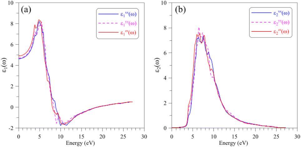 | ||
| Fig. 4 Dielectric function including (a) real part ε1(ω) and (b) imaginary part ε1(ω) of the AgGaGeS4 crystal obtained by DFT calculations within the TB-mBJ+U method. | ||
However, the magnitudes of these peaks vary slightly depending on the direction of the incident waves due to the anisotropy of the AgGaGeS4 crystal. In the energy interval 3–5 eV, the real dielectric component along the y-axis, ε1yy(ω), is the lowest by intensity; therefore, the reflectivity of AgGaGeS4 along the y-direction is supposed to be the lower than in the x- and z-directions. The shifts of the ε1(ω) peaks are observed mainly in the energy ranges 3–6 eV and 8–12 eV. Therefore, the intensity of the reflected waves by AgGaGeS4 not only depends on the direction but also on the energy of the EM waves. The polarization of the imaginary part ε2(ω) of the dielectric function occurs at energy intervals 3–4.5 eV and 5.5–16.5 eV corresponding to the highest permanent absorption of the EM waves whose wavelengths are in ranges 257–413 nm, and 75–225 nm, respectively. One of the consequences of permanent absorbing EM waves is to excite the electrons from the valence band to the conduction band. Therefore, the main peaks/features of the ε2(ω) function located near 3.5 eV, 6 eV, 7 eV and 9 eV originate due to the transition of electrons from S-p orbitals in the valence band to the Ge-s orbitals in the conduction band.
Regarding to the optical properties of the AgGaGeS4 crystal, it is well-known that the square root of the dielectric function ε(ω) gives the refraction index in the form of complex numbers, where real part n(ω) is related to how the EM waves are slowed down and inclined in materials, and the imaginary part k(ω) describes how fast the energy of EM waves vanishes in materials. As shown in Fig. 5(a and b), the shapes of spectra of the refractive index and the extinction coefficient, n(ω) and k(ω), are similar to those of the ε1(ω) and ε2(ω) spectra, respectively (cf. Fig. 4(a and b)). The spectrum of the refractive index n(ω) as presented in Fig. 5(a) reaches its highest peaks in the energy range of 3–7 eV signifying the range of EM waves which are essentially inclined and reflected by the AgGaGeS4 crystal. The EM waves at slightly higher energy levels, 7–12 eV, according to Fig. 5(b), are likely to vanish in the AgGaGeS4 crystal. At higher energy levels, 17–23 eV, most energy of the incident EM waves will be lost. The electron energy-loss spectrum L(ω) presented in Fig. 5(c) reveals the existence of a maximum centered at around 19.5 eV. This value corresponds to plasma frequency of the AgGaGeS4 crystal. The reflectivity spectrum R(ω), shown in Fig. 5(d), reveals high values in the energy range of 5–7 eV as the result of the absorption and re-emit effects governed by the n(ω) and k(ω) parameters. The direction-dependence of the R(ω) function is also obvious in this energy range, where the reflectivity along the z-direction is the highest followed by reflectivity along the x- and y-directions. At energy levels higher than 17 eV, the reflectivity of AgGaGeS4 decreases abruptly due to the sharp increase of the energy-loss (Fig. 5(c)).
 | ||
| Fig. 5 Optical parameters such as (a) refractive index n(ω), (b) extinction coefficient k(ω), (c) electron energy-loss spectrum L(ω), and (d) optical reflectivity R(ω) of the AgGaGeS4 crystal obtained by DFT calculations within the TB-mBJ+U method. | ||
The absorption coefficient α(ω) of AgGaGeS4, as shown in Fig. 6, is neglectable for the EM waves whose energies are smaller than 2.5 eV. Therefore, AgGaGeS4 is transparent for the most part of the visible light. Starting from 2.5 eV, the absorption increases slightly and reaches its fast increase in the vicinity of 3.4 eV, which is determined as the theoretical band gap of the AgGaGeS4 crystal. The polarization of the α(ω) spectrum is minor up to the energy range where the absorption coefficient α(ω) reaches the highest values (above 106 cm−1). These highest values of the α(ω) spectrum are detected in the energy range of 7–12 eV. This energy range is located inside the energy range of 5.5–16.5 eV, where the ε2(ω) function possesses its highest values. Consequently, it is expected that the AgGaGeS4 crystal strongly absorbs the EM waves with the wavelengths being in range of 103–177 nm. At these wavelengths, the α(ω) function is strongly polarized: the αzz(ω) component reveals higher intensity as compared to those of the other two remaining directions. The EM waves shorter than 61 nm are weakly absorbed by AgGaGeS4 and the crystal is almost transparent up to ultra-violet lights.
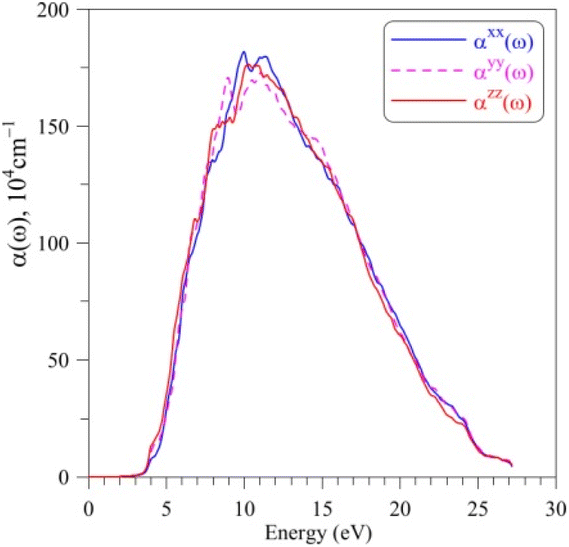 | ||
| Fig. 6 Absorption coefficient α(ω) AgGaGeS4 crystal calculated by the TB-mBJ+U method. | ||
5 Conclusions
The first-principles calculations using PBE, PBE+U, and TB-mBJ+U methods were performed to study the electronic and optical properties of the AgGaGeS4 crystal. Results of the present DFT calculations within the TB-mBJ+U method are found to be in the best agreement with the experiments based on XPS and XES measurements. In particular, in accordance with the present first-principles band-structure calculations, S 3p states are located mainly at the top and in the upper part of the AgGaGeS4 valence band, with essential contributions of these electronic states throughout the whole band region ranging from −6.1 to 0 eV, Ag 4d and Ge 4p states contribute mainly in the central part of the band, while Ga 4p states in its upper portion. The present theoretical predictions have been supported by measurements of the X-ray emission bands giving information on peculiarities of the energy distribution of the electronic S 3p, Ag 4d, Ga 4p and Ge 4p states, the main contributors to the valence band of AgGaGeS4. Some peculiar hybridization of the mentioned electronic states is observed in the AgGaGeS4 valence band suggesting the existence of essential covalent constituent (in addition to the ionic one) of the chemical bonding in the AgGaGeS4 crystal. The bottom of the conduction band of AgGaGeS4, in accordance with our DFT calculations, is mainly formed by unoccupied Ge-s states, with smaller contributions of unoccupied Ga-s, Ag-s and S-p states, too. Plasma frequency of the AgGaGeS4 crystal is equal to about 19.5 eV. The electromagnetic waves shorter than 61 nm are weakly absorbed by AgGaGeS4 and the crystal is almost transparent up to ultra-violet light.Conflicts of interest
There are no conflicts to declare.References
- J. Šulc and H. Jelínková, Solid-state lasers for medical applications, Lasers for medical applications, Elsevier 2013, pp. 127–176 Search PubMed.
- D. Kochiev, A. Prokhorov, A. Lukashev, I. Hcherbakov and S. Vartapetov, Surgical solid-state lasers and their clinical applications, Handbook of Solid-State Lasers, Elsevier 2013, pp. 572–597 Search PubMed.
- V. Petrov, Opt. Mater., 2012, 34, 536–554 CrossRef.
- H. Hügel, Opt. Lasers Eng., 2000, 34, 213–229 CrossRef.
- K. Pribil and J. Flemmig, Solid state laser communications in space (SOLACOS) high data rate satellite communication system verification program, Space Optics 1994, Space Instrumentation and Spacecraft Optics, SPIE, 1994, pp. 39–48 Search PubMed.
- G. Edwards, R. Logan, M. Copeland, L. Reinisch, J. Davidson, B. Johnson, R. Maciunas, M. Mendenhall, R. Ossoff and J. Tribble, Nature, 1994, 371, 416–419 CrossRef PubMed.
- H. R. Aldag, Solid state dye laser for medical applications, Visible and UV Lasers, SPIE 1994, pp. 184–189 Search PubMed.
- L.-H. Li, J.-Q. Li and L.-M. Wu, J. Solid State Chem., 2008, 181, 2462–2468 CrossRef.
- A. Godard, C. R. Phys., 2007, 8, 1100–1128 CrossRef.
- J. Kim and T. Hughbanks, Inorg. Chem., 2000, 39, 3092–3097 CrossRef.
- V. Dmitriviev, G. Gurzadyan and D. Nikogosyan, Handbook of Nonlinear Crystals, Springer, Berlin, 1999 Search PubMed.
- B. Levine, Phys. Rev. B: Solid State, 1973, 7, 2600 CrossRef CAS.
- J. Sulc, H. Jelinkova, J. K. Jabczynski, W. Zendzian, J. Kwiatkowski, K. Nejezchleb and V. Skoda, Comparison of diode-side-pumped triangular Nd: YAG and Nd: YAP laser, Solid State Lasers XIV: Technology and Devices, SPIE 2005, pp. 325–334 Search PubMed.
- O. Guillot-Noël, B. Bellamy, B. Viana and D. Vivien, Phys. Rev. B: Condens. Matter Mater. Phys., 1999, 60, 1668–1677 CrossRef.
- T. Pollak, W. Wing, R. Grasso, E. Chicklis and H. Jenssen, IEEE J. Quantum Electron., 1982, 18, 159–163 CrossRef.
- H. Rast, H. Caspers and S. Miller, Phys. Rev., 1968, 169, 705 CrossRef CAS.
- K. Regelskis, J. Želudevičius, N. Gavrilin and G. Račiukaitis, Opt. Express, 2012, 20, 28544–28556 CrossRef CAS PubMed.
- X. Zhao, S. Zhu, B. Zhao, B. Chen, Z. He, R. Wang, H. Yang, Y. Sun and J. Cheng, J. Cryst. Growth, 2008, 311, 190–193 CrossRef CAS.
- P. Canarelli, Z. Benko, A. Hielscher, R. Curl and F. Tittel, IEEE J. Quantum Electron., 1992, 28, 52–55 CrossRef CAS.
- G. Bhar and R. Smith, IEEE J. Quantum Electron., 1974, 10, 546–550 CAS.
- G. Boyd, E. Buehler and F. Storz, Appl. Phys. Lett., 1971, 18, 301–304 CrossRef CAS.
- J. Petit, S. A. S. Hassani, P. Galtier, A. Godard, M. Raybaut and M. Lefebvre, Progress in ZnGeP2 and AgGaS2 crystal growth: first results on difference-frequency generation and optical parametric oscillation, Optical Materials in Defence Systems Technology VI, SPIE, 2009, pp. 132–139 Search PubMed.
- N.-H. Kim, D. H. Shin and R. S. Feigelson, Mater. Sci. Eng., B, 1996, 38, 229–235 CrossRef.
- R. Eckardt, Y. Fan, R. Byer, R. Route, R. Feigelson and J. Van der Laan, Appl. Phys. Lett., 1985, 47, 786–788 CrossRef CAS.
- W. Huang, Z. He, B. Zhao, S. Zhu and B. Chen, J. Alloys Compd., 2019, 796, 138–145 CrossRef.
- W. Huang, Z. He, S. Zhu, B. Zhao, B. Chen and S. Zhu, Inorg. Chem., 2019, 58, 5865–5874 CrossRef PubMed.
- P. G. Schunemann, K. T. Zawilski and T. M. Pollak, J. Cryst. Growth, 2006, 287, 248–251 CrossRef.
- Y. Andreev, P. Geiko, V. Badikov, G. Bhar, S. Das and A. Chaudhury, MCLC S&T, Sect. B: Nonlinear Opt., 2002, 29, 19–27 Search PubMed.
- K. Miyata, V. Petrov and K. Kato, Appl. Opt., 2007, 46, 5728–5731 CrossRef.
- V. Petrov, V. Badikov, G. Shevyrdyaeva, V. Panyutin and V. Chizhikov, Opt. Mater., 2004, 26, 217–222 CrossRef.
- M. Shevchuk, V. Atuchin, A. Kityk, A. Fedorchuk, Y. Romanyuk, S. Całus, O. Yurchenko and O. Parasyuk, J. Cryst. Growth, 2011, 318, 708–712 CrossRef.
- I. Olekseyuk, A. Gulyak, L. Sysa, G. Gorgut and A. Lomzin, J. Alloys Compd., 1996, 241, 187–190 CrossRef CAS.
- G. Y. Davydyuk, G. Myronchuk, G. Lakshminarayana, O. Yakymchuk, A. Reshak, A. Wojciechowski, P. Rakus, N. AlZayed, M. Chmiel and I. Kityk, J. Phys. Chem. Solids, 2012, 73, 439–443 CrossRef CAS.
- O. Y. Khyzhun, O. V. Parasyuk and A. O. Fedorchuk, Adv. Alloys Comp., 2013, 1, 15–29 Search PubMed.
- P. Blaha, K. Schwarz, F. Tran, R. Laskowski, G. K. H. Madsen and L. D. Marks, J. Chem. Phys., 2020, 152, 074101 CrossRef CAS.
- J. P. Perdew, K. Burke and M. Ernzerhof, Phys. Rev. Lett., 1997, 78, 1396 CrossRef CAS.
- D. Koller, F. Tran and P. Blaha, Phys. Rev. B: Condens. Matter Mater. Phys., 2012, 85, 155109 CrossRef.
- V. I. Anisimov, I. V. Solovyev, M. A. Korotin, M. T. Czyżyk and G. A. Sawatzky, Phys. Rev. B: Condens. Matter Mater. Phys., 1993, 48, 16929–16934 CrossRef CAS PubMed.
- P. Novák, F. Boucher, P. Gressier, P. Blaha and K. Schwarz, Phys. Rev. B: Condens. Matter Mater. Phys., 2001, 63, 235114 CrossRef.
- A. B. Shick, A. I. Liechtenstein and W. E. Pickett, Phys. Rev. B: Condens. Matter Mater. Phys., 1999, 60, 10763–10769 CrossRef CAS.
- E. R. Ylvisaker, W. E. Pickett and K. Koepernik, Phys. Rev. B: Condens. Matter Mater. Phys., 2009, 79, 035103 CrossRef.
- C. Ambrosch-Draxl and J. O. Sofo, Comput. Phys. Commun., 2006, 175, 1–14 CrossRef CAS.
- F. Wooten, Am. J. Phys., 1973, 41, 939–940 CrossRef.
- C. Ambrosch-Draxl, J. A. Majewski, P. Vogl and G. Leising, Phys. Rev. B: Condens. Matter Mater. Phys., 1995, 51, 9668–9676 CrossRef CAS PubMed.
- A. Meisel, G. Leonhardt and R. Szargan, X-Ray Spectra and Chemical Binding, Springer-Verlag, Berlin/Heidelberg, 1989 Search PubMed.
- O. Y. Khyzhun, Y. V. Zaulychny and E. A. Zhurakovsky, J. Alloys Compd., 1996, 244, 107–112 CrossRef CAS.
- V. L. Bekenev, V. V. Bozhko, O. V. Parasyuk, G. E. Davydyuk, L. V. Bulatetska, A. O. Fedorchuk, I. V. Kityk and O. Y. Khyzhun, J. Electron Spectrosc. Relat. Phenom., 2012, 185, 559–566 CrossRef CAS.
- P. D. C. King, T. D. Veal, C. F. McConville, F. Fuchs, J. Furthmüller, F. Bechstedt, J. Schörmann, D. J. As, K. Lischka, H. Lu and W. J. Schaff, Phys. Rev. B: Condens. Matter Mater. Phys., 2008, 77, 115213 CrossRef.
- I. D. Olekseyuk, A. V. Gulyak, L. V. Sysa, G. P. Gorgut and A. F. Lomzin, J. Alloys Compd., 1996, 241, 187–190 CrossRef CAS.
- R. E. Nikolaev and R. G. Vasilyeva, J. Solid State Chem., 2013, 203, 340–344 CrossRef CAS.
- W. Huang, Z. He, S. Zhu, B. Zhao, B. Chen and S. Zhu, Inorg. Chem., 2019, 58, 5865–5874 CrossRef CAS PubMed.
- M. Kavčič, J. C. Dousse, J. Szlachetko and W. Cao, Nucl. Instrum. Methods Phys. Res. B, 2007, 260, 642–646 CrossRef.
- U. Eiichirou, K. Jun and M. Uda, Nucl. Instrum. Methods Phys. Res. B, 1993, 75, 24–27 CrossRef.
- A. S. Krymus, I. V. Kityk, P. Demchenko, O. V. Parasyuk, G. L. Myronchuk, O. Y. Khyzhun and M. Piasecki, Mater. Res. Bull., 2017, 95, 177–184 CrossRef.
| This journal is © The Royal Society of Chemistry 2023 |