DOI:
10.1039/D2RA07487G
(Paper)
RSC Adv., 2023,
13, 2301-2310
Two-dimensional H– and F–BX (X = O, S, Se, and Te) photocatalysts with ultrawide bandgap and enhanced photocatalytic performance for water splitting†
Received
24th November 2022
, Accepted 27th December 2022
First published on 16th January 2023
Abstract
We theoretically propose a type of monolayer structure, H– or F–BX (X = As, Sb; Y = P, As), produced by surface hydrogenation or fluorination, with high stability, large band structures and high light absorption for photocatalytic water splitting. Based on first-principles calculations with the HSE06 functional, the electronic properties and optical properties were explored to reveal their potential performance in semiconductor devices. Additionally, owing to the Janus structure and high electronegativity of the monolayers, our calculations showed that surface fluorination can easily create an internal electric field compared with surface hydrogenation, which results in different trends of increasing bandgaps in monolayer H– and F–BX. We also found that the monolayers H– and F–BX have suitable band edges and high solar to hydrogen (STH) efficiency, enabling them to be photocatalysts for water splitting. Our work not only proposes eight monolayer semiconductors for expanding the number of two-dimensional semiconductors, but also provides a guide for how to regulate semiconductors for application in photocatalytic water splitting by using surface hydrogenation and fluorination.
1. Introduction
Since the successful isolation of graphene,1–3 resulting in potential candidates for developing high performance electronic and optoelectronic nano-devices, the exploration of more novel 2D materials with various properties has attracted intense research interest. There are numerous 2D materials that have been reported, such as phosphorene,4–8 MXenes,9–11 transition metal dichalcogenides (TMDCs),12–19 and silicene.20–25 The use of these 2D materials in field-effect transistors, quantum devices, and energy storage, as well as conversion applications, has demonstrated excellent potential. In particular, because of their ultrathin atomic thickness and large specific surface area, these 2D materials are considered appealing candidates for use in flexible electronic devices26–28 and photocatalysts.29–35 However, the current 2D materials have two obvious drawbacks. First, although there are a few 2D materials with ultrawide bandgaps (>3.40 eV), the majority of 2D pristine materials have bandgaps between 0 and 3.40 eV,36–40 which limits their application in high-energy and high-frequency devices as well as insulators. Second, due to the rigorous constraints of band structures, optical absorption, exciton recombination behaviors, and stability, there are only a few 2D materials, such as monolayer SiP2 and B6P2, that perform well in photocatalytic water splitting.41–44 Due to the lack of 2D materials for high-energy and high-frequency devices, more effort should be made to investigate more 2D materials for use in ultrawide bandgap technologies and photocatalytic water splitting.
Recently, first-principles calculation has grown in importance. It can be separated into two parts. One part is the design of whole new structures, which is critical for enriching 2D materials,45,46 and the second part is the creation of new models and improvement of their performance by applying doping, heterojunction, or surface modifications.47–53 Due to the recent discovery of countless new 2D models, the first part is becoming increasingly challenging. Therefore, the second part is becoming more popular. Hydrogenation and fluorination are recognized as common but effective surface modification methods to tune the structures and properties of newly discovered materials. For example, the hydrogenation and fluorination of graphene can result in bandgaps of approximately 4.00 and 3.13 eV, respectively.53–56 In addition, applying hydrogenation to the top side of bilayer h–BN and fluorination to its bottom side simultaneously can form a new metal-free Janus photocatalyst that can drive infrared-light photocatalytic water splitting.57 Furthermore, hydrogenation can also improve the stability of monoatomic-layer MX (M = Ga and In, X = S, Se, and Te) nanosheets.46 In comparison to the bandgaps of typical monolayer MX, the bandgaps of hydrogenated MX nanosheets are direct and larger. As a result, we are driven to try to create new 2D structures with ultrawide bandgaps and appropriate efficiency for photocatalytic water splitting via surface hydrogenation and fluorination. If the outcome is favorable, it will encourage the development of 2D materials in ultrawide bandgap technology and photocatalytic water splitting.
Based on first-principles density functional theory, we have theoretically proposed the monolayers H– and F–BX (X = O, S, Se, and Te) by applying hydrogenation and fluorination to monoatomic-layer hexagonal BX. The binding energies and phonon spectra of these nanosheets were analyzed to identify their dynamics and energy stability. The calculations of their band structures and densities of states were performed to study their electronic structure properties. Furthermore, the edge levels, work functions, optical absorption spectra, and solar to hydrogen (STH) efficiencies of the H– and F–BX monolayers were studied to explore their performance in optical devices and photocatalysts for water splitting.
2. Computational details
Our entire analysis was based on first-principles density functional theory. The Vienna Ab initio Simulation Package (VASP)58 was used to calculate structure optimizations, band structures, densities of states, and optical absorption spectra, utilizing projector-augmented-wave pseudopotentials.59 The plane-wave cutoff energy was set to 500 eV. To relax our structure models, we used the generalized gradient approximation expressed by the Perdew–Burke–Ernzerhof (PBE) functional.60 Once fully relaxed, the forces in the optimized monolayers H– and F–BX were less than 0.001 eV Å−1 and the energy tolerances were less than 1 × 10⁻⁸ eV per atom. A 20 Å vacuum layer was adopted between adjacent layers. In the Monkhorst–Pack system,61 the Brillouin zone was represented by a 6 × 6 × 1 k-point sample.61 For studying the electrical structures and optical properties, the Heyd–Scuseria–Ernzerhof (HSE06) hybrid functional was used.62 The phonon spectra of the monolayers were computed using the Cambridge Series of Total Energy Package (CASTEP) and linear response approach.63,64 The norm-conserving pseudopotentials and a plane-wave cutoff energy of 940 eV were employed in the phonon spectra computations, while the other settings were the same as in VASP setting.
3. Results and discussion
3.1 Rationality and stability of monolayer H– and F–BX structures
From Fig. S2(a)–(d),† we can see that all the phonon spectra of monoatomic-layer BX (X = O, S, Se, and Te) clearly show a soft model in their Brillouin zones, thus we can confirm that monoatomic-layer hexagonal BX (X = O, S, Se, and Te) is unstable. In typical monolayer B2X2, two monoatomic-layer hexagonal BX structures stack directly, and the top sub-layer's B atoms connect with the bottom sub-layer's B atoms to saturate each other's unpaired electrons. As a result, we can use H and F atoms to saturate the unpaired electrons of the B atoms, resulting in the formation of new monolayers H– and F–BX (X = O, S, Se, and Te), as shown in Fig. 1(a) and (b). The lattice parameters of the monolayers H– and F–BX after optimization of their entire structures are presented in Table 1. As can be seen in Fig. 1(a) and (b), the B2X2 monolayer clearly shows two different sublayers, an H or F sublayer and an X (X = O, S, Se, and Te) sublayer. This unique asymmetric geometry results in an out-of-plane built-in electric field of up to 0.96–1.31 Debye, as listed in Table 1. From looking at the dipoles of the H– and F–BX monolayers, we find that the dipoles of the F–BX monolayers are higher than those of the corresponding H–BX monolayers due to the strong electronegativity of the F atom. Meanwhile, the dipoles of the H– and F–BX monolayers increase with the decrease of the electronegativity of the X atom. Furthermore, the increase of the dipoles in the H–BX monolayers happens faster than that in the F–BX monolayers, which may further influence the change of the band structure. Although the monolayers H– and F–BX have suitable bonding character, further research into their energy and dynamics stability is required. To study the energy stability of the monolayers H– and F–BX, we calculated two types of binding energies (Eb). The first type Eb1 is a typical one, which is calculated by the following formula:| |
 | (1) |
where Etot is the total energy of the monolayers H– and F–BX and Eatom is the energy of the free atoms. The results are shown in Table 1. The Eb1 values of the eight monolayers reveal that the monolayers H– and F–BX may have stable energies owing to their low binding energies. More evidence should be provided to support the claim that these eight monolayers have stable energies. Then, we calculated Eb2, which can provide the strength values of the H– or F–B bonds. The corresponding formula is as follows:| | |
Eb2 = Etot − E(BX) − Eatom(HorF)
| (2) |
where E(BX) is the total energy of the monoatomic-layer hexagonal BX (X = O, S, Se, and Te) after full relaxation. The Eb2 values of the monolayers H– and F–BX are shown in Table 1. We also calculated the Eb2 values of the monolayer B2X2 (X = O, S, Se, and Te), which show the bond energies of the B–B bonds. The corresponding formula is as follows:where Etot is the total energy of the monolayer B2X2. The Eb2 values of the monolayers B2O2, B2S2, B2Se2, and B2Te2 are −4.32, −3.65, −3.88, and −3.47 eV, respectively. It is clear that the Eb2 values of the monolayer B2X2 are higher than those of the H– and F–BX monolayers. This means that H and F atoms bonding with the monoatomic-layer hexagonal BX are more stable than BX bonding with BX. Thus, we confirm that the monolayers H– and F–BX have stable energies.
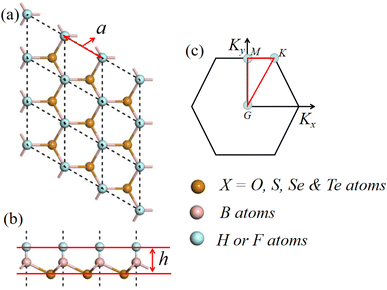 |
| | Fig. 1 (a) and (b) Structure model of the monolayers H– and F–BX (X = O, S, Se, and Te) and (c) Brillouin zone of monolayer H– and F–BX (X = O, S, Se, and Te) with high-symmetry points. | |
Table 1 The lattice constants and two types of binding energy in the monolayers H– and F–BX (X = O, S, Se, and Te)
| |
H–BO |
H–BS |
H–BSe |
H–BTe |
F–BO |
F–BS |
F–BSe |
F–BTe |
| a (Å) |
2.46 |
3.06 |
3.27 |
3.59 |
2.53 |
3.10 |
3.32 |
3.65 |
| h (Å) |
1.74 |
2.00 |
2.08 |
2.17 |
1.88 |
2.19 |
2.27 |
2.37 |
| Eb1 (eV per atom) |
−6.32 |
−5.07 |
−4.78 |
−4.46 |
−6.97 |
−5.73 |
−5.45 |
−5.10 |
| Eb2 (eV) |
−5.87 |
−5.43 |
−5.57 |
−5.32 |
−7.82 |
−7.42 |
−7.57 |
−7.23 |
| p (Debye) |
0.02 |
0.44 |
0.67 |
0.96 |
0.91 |
0.84 |
0.94 |
1.31 |
Fig. 2 shows the phonon spectra of the monolayers H– and F–BX, which are expected to indicate the dynamics stability. The phonon spectra without imaginary frequencies strongly indicate that the monolayers H– and F–BX have stable dynamics. Fig. 2 shows nine lattice wave branches in all the phonon spectra and a lack of imaginary frequencies in all the acoustic branches. Although we are unable to provide more evidence for monolayer thermodynamic stability and other types of stability owing to limited computing resources, the study of the binding energies and phonon spectra clearly indicates that the monolayers H– and F–BX are stable.
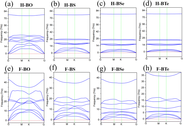 |
| | Fig. 2 Phonon spectra of monolayers H– and F–BX (X = O, S, Se, and Te). | |
3.2 Electronic band structures of the monolayers H– and F–BX
Fig. 3 illustrates the band structures of the monolayers H– and F–BX as simulated by the HSE06 hybrid functional. Fig. 3(a) and (e) demonstrates that the bandgaps of the insulators H–BO and F–BO are 8.58 eV and 9.63 eV, respectively. The H–BS (4.36 eV), H–BSe (4.56 eV), F–BS (5.00 eV), and F–BSe (4.06 eV) are indirect, ultrawide bandgap semiconductors (>3.40), as shown in Fig. 3(b), (c), (f) and (g). Additionally, the H–BTe and F–BTe (see Fig. 3(d) and (h)) are indirect, large bandgap semiconductors with values of 3.30 and 2.62 eV, respectively. From the bandgaps of F–BX and H–BX, we notice that bandgaps of the F–BX monolayers change faster than those of H–BX, resulting in the bandgap of H–BO being smaller than that of F–BO, but the bandgap of H–BTe being larger than that of F–BTe. These different trends in the bandgaps could be caused by the different trends of the increase of the built-in electric field. Meanwhile, we also found that the valence band maximum (VBM) of F–BO is located at the G point, whereas the VBM of H–BO occurs along the K–G direction. The conduction band minimum (CBM) values of both H–BO and F–BO lie at the G point. All the VBM values of the other monolayers H– and F–BX lie at the G point, while all their CBM values lie at the M point. For the above band structure analysis, the corresponding Brillouin zone of H–BO and F–BO with high-symmetry points can be seen in Fig. 1(c). We also calculated the band structure of the 1T-phase B2X2 as shown in Fig. S3† and the bandgaps of the B2X2 monolayers match well with those found in previous work.67,68 Compared with the corresponding monolayer B2X2, the monolayers H– and F–BX have much larger bandgaps, implying that hydrogenation and fluorination of monoatomic-layer hexagonal BX can enlarge their bandgaps and broaden their applications in insulator and semiconductor technologies.
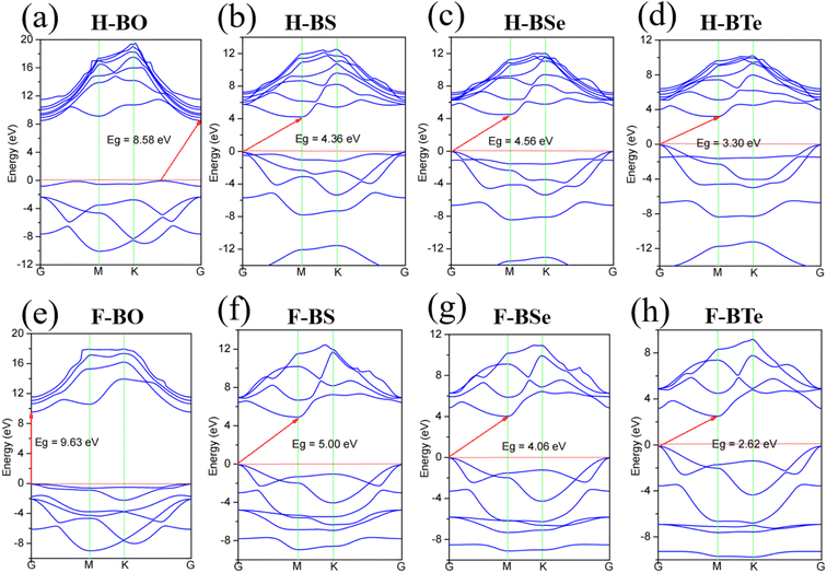 |
| | Fig. 3 Band structures of the monolayers H– and F–BX (X = O, S, Se, and Te). | |
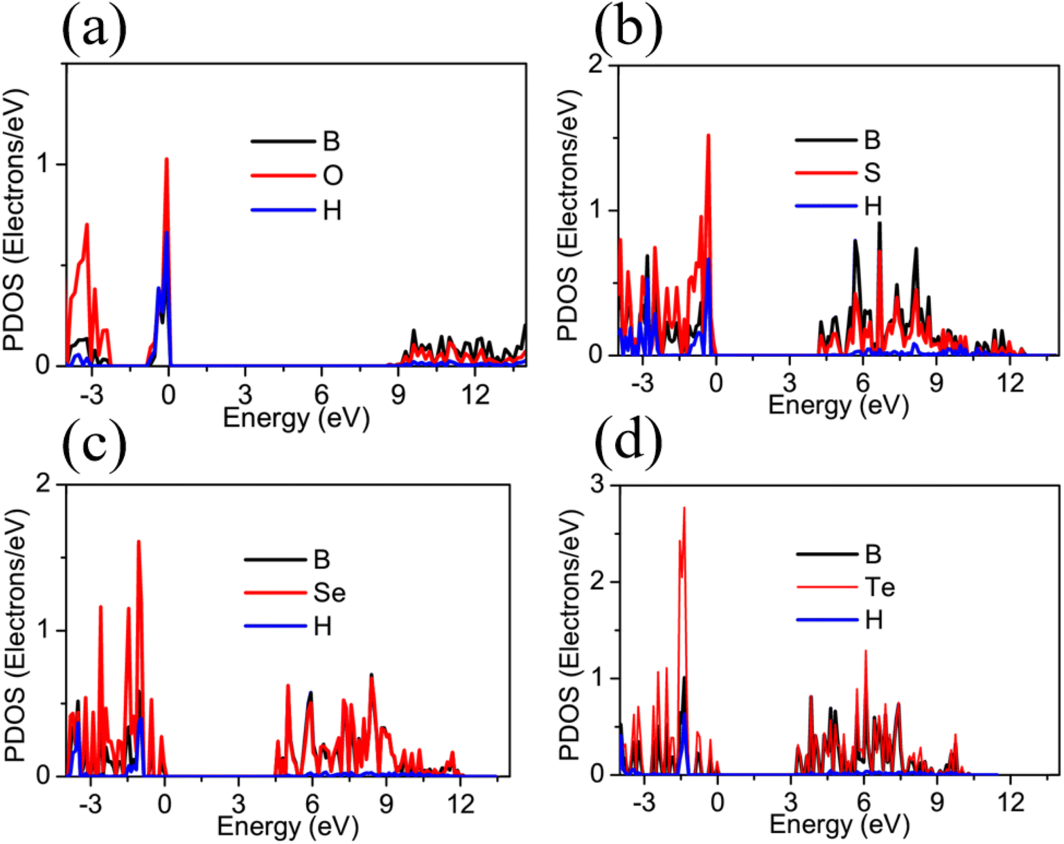
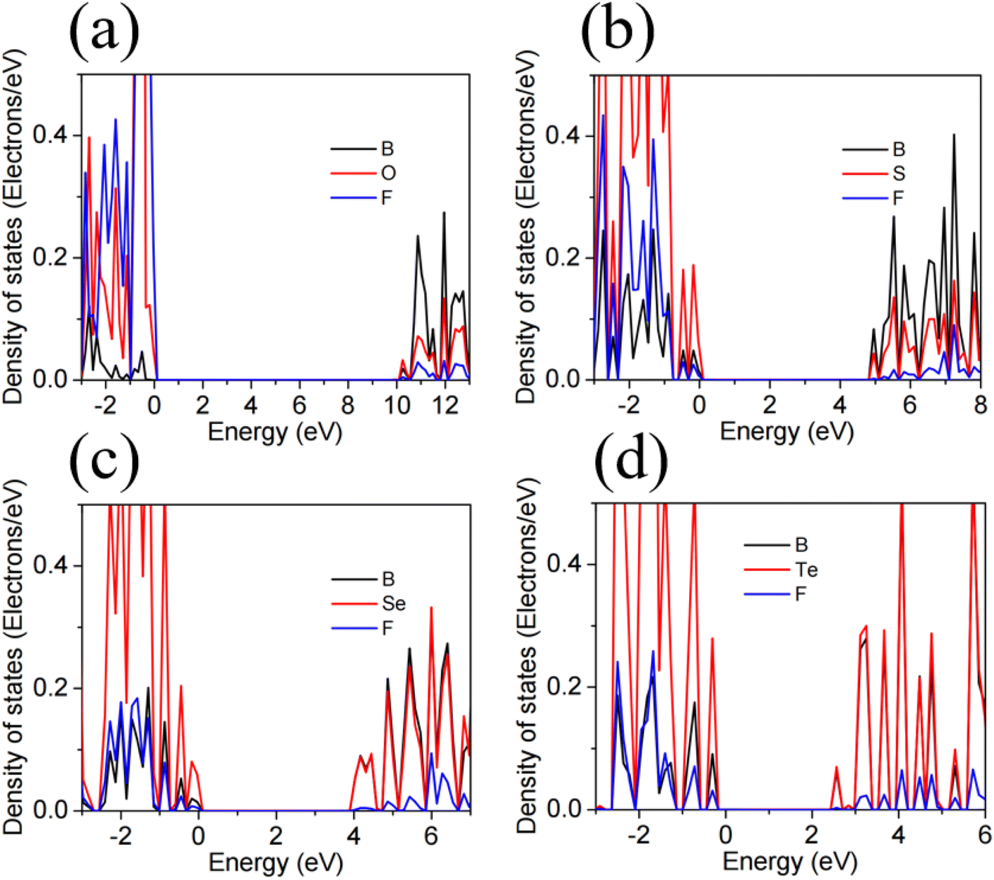
As shown in Fig. 4 and 5, we calculated the projected density of states (PDOS) of the monolayers H– and F–BX in order to determine the contribution of each atom to the electronic states. For H–BO and H–BS (shown in Fig. 4(a) and (b), respectively), the occupied states near the VBM are filled by B, O (S), and H atoms, while their occupied states near the CBM are mainly filled by B and O (S) atoms. Fig. 4(c) and (d) demonstrates that B and Se (Te) atoms are significant contributors to the occupied states adjacent to the VBMs and CBMs, while H atoms are practically insignificant. Therefore, as shown in Fig. 4, the carriers in H–BX mainly transport on the BX planes, which may cause a hard separation of electron and hole pairs. For F–BX, the occupied states near the VBM and CBM, as shown in Fig. 5, are also mainly contributed to by B and X atoms. However, in contrast to H–BX, although it is not so strongly, F atoms in F–BX contribute to the occupied states near the VBM and CBM, which means that F atoms can provide carriers. Due to the noncoplanarity of the B, X, and F atoms, these phenomena allow F–BX to be more effective as a photocatalyst for separating electrons and holes.
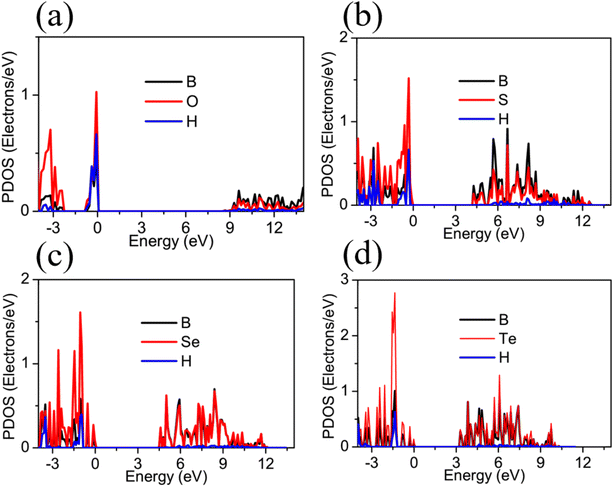 |
| | Fig. 4 PDOS of the monolayer H–BX (X = O, S, Se, and Te). | |
 |
| | Fig. 5 PDOS of the monolayer F–BX (X = O, S, Se, and Te). | |
3.3 Optical and photocatalytic properties of the monolayers H– and F–BX
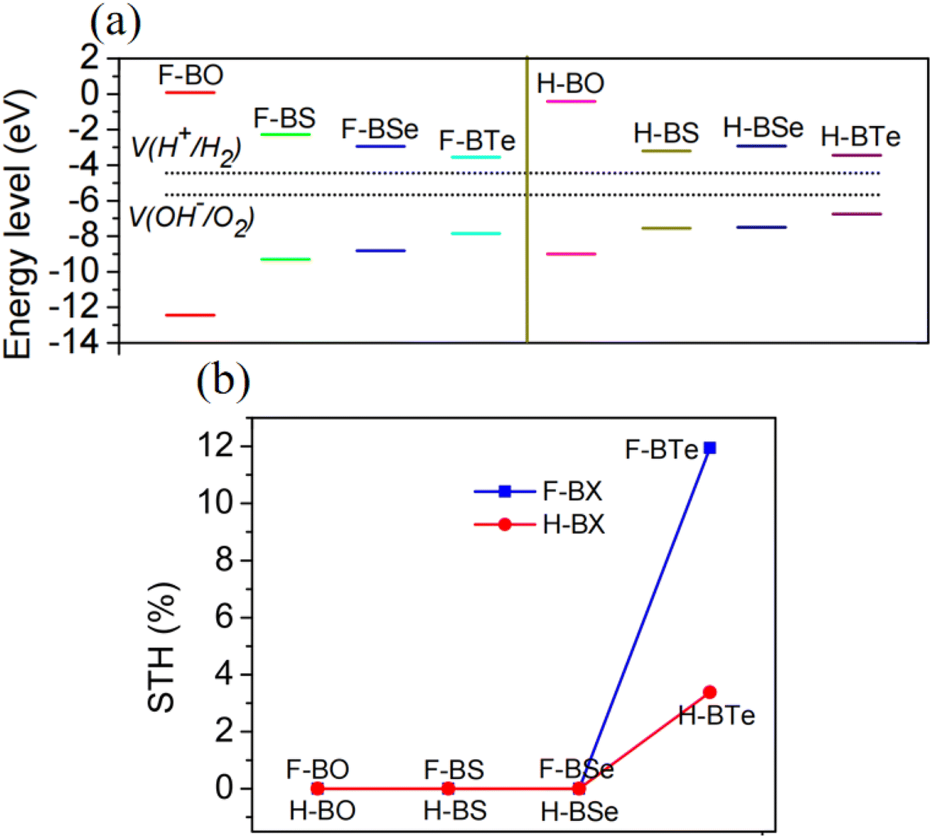
Due to their large bandgaps, the monolayers H– and F–BX are likely to be suitable photocatalysts for water splitting. Thus, calculating the work function of these eight monolayers allowed us to determine the vacuum level alignment of the band edge levels, as shown in Fig. 6(a). When we calculated the work function, we applied the dipole correction owing to the Janus structures of the monolayers H– and F–BX. Fig. 6(a) indicates that all the monolayers H– and F–BX have a large work function (>6.0 eV). In combination with their large enough bandgaps as mentioned above, we propose that these monolayers may be used in photocatalytic water splitting. Furthermore, it is interesting to note that the work functions of the monolayer F–BX for the top (F atoms) and bottom (B and X atoms) sides are different. In contrast, the work functions of the monolayer H–BX on the top (H atoms) and bottom (B and X atoms) sides are the same. This phenomenon will cause the monolayers F–BX and H–BX to exhibit different photocatalytic mechanisms. The monolayer H–BX utilizes the conventional photocatalytic mechanism and is anticipated to be used in photocatalytic water splitting, as shown in Fig. 6(c). Fig. 6(c) demonstrates that in semiconductor photocatalysts, the CBM relative to the vacuum level must be lower than the oxidation potential [V(O2/H2O) = −5.67 eV] and the VBM relative to the vacuum level must be greater than the reduction potential [V(H2/H+) = −4.44 eV]. The Janus photocatalytic process used by the monolayer F–BX is depicted in Fig. 6(b), and it shows that the internal electric field and vacuum level difference will help separate electrons and holes on the top and bottom sides and increase the driving energy of the redox reaction in water splitting. Next, we will study the photocatalytic properties of the monolayers H– and F–BX for water splitting.
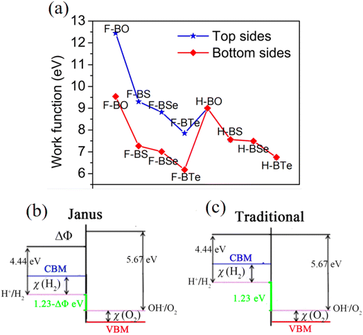 |
| | Fig. 6 (a) Work function of the monolayers H– and F–BX (X = O, S, Se, and Te) on the top sides and bottom sides; (b) energy level diagram for photocatalytic water splitting, which is suitable for the monolayer F–BX (X = O, S, Se, and Te); and (c) schematic diagram suitable for the monolayer H–BX (X = O, S, Se, and Te). | |
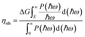
As can be seen in Fig. 7(a), comparing the CBM and VBM of the monolayers H– and F–BX with the redox potentials in water splitting, the band edge positions of the monolayers H– and F–BX match with the band structure requirements for photocatalytic water splitting. Additionally, Fig. 7(a) demonstrates that every monolayer of H– and F–BX has a sufficiently large driving energy value (>0.4 eV) to support both the reduction of H2O to O2 and H+ to H2. According to this discovery, the monolayers H– and F–BX might be thought of as potential 2D semiconductors for photocatalytic water splitting. However, even though these monolayers meet the band structure requirements for photocatalytic water splitting, it is still vital to consider the solar to hydrogen efficiency and optical absorption, which are crucial standards for the photocatalytic efficiency. The STH efficiency (ηsth) of the monolayer H–BX can be calculated by the following formula:65
| |
 | (4) |
where
P(
ħω) denotes the AM1.5G solar energy flux, which varies with photon energy
ħω, and Δ
G is set to 1.23 eV. The minimum energy
E of the photons is given as follows:
| |
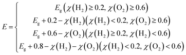 | (5) |
where
Eg is the bandgap of the monolayer H–BX,
χ(O
2) denotes the driving energy of reactions involving the evolution of oxygen, and
χ(H
2) denotes the driving energy of reactions involving the evolution of hydrogen, which can be seen in
Fig. 6(b) and (c). The STH efficiencies of H–BO, H–BS, and H–BSe tend to zero, whereas the H–BTe has a STH efficiency value of 3.38%, as shown in
Fig. 7(b). The monolayer H–BX (X = O, S, Se, and Te) exhibits unsatisfactory performance because of large bandgaps. The STH efficiency of the monolayer F–BX needs to be adjusted because of its internal electric field, which influences electron–hole separation during photocatalytic water splitting in a positive way:
66| |
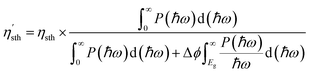 | (6) |
where Δ
Φ (shown in
Fig. 6(b)) is the electrostatic potential difference defined as |
Vbottom −
Vtop|.
Fig. 7(b) indicates that the STH efficiencies of F–BO, F–BS, and F–BSe also tend to zero owing to their large bandgaps. However, the STH efficiency of F–BTe reaches 11.94% (>10%), which means that it has certain economic value when applied in photocatalytic hydrogen production.
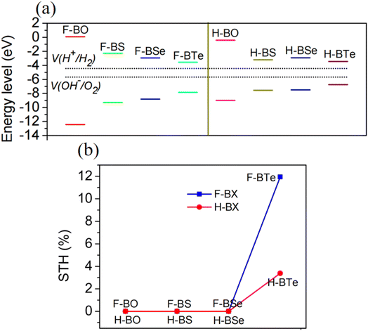 |
| | Fig. 7 (a) VBM and CBM of the monolayers H– and F–BX (X = O, S, Se, and Te) compared with the standard redox potentials for water splitting and (b) STH efficiency of the monolayers H– and F–BX (X = O, S, Se, and Te). | |
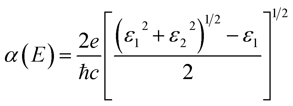
Additionally, as can be seen in Fig. 8, we estimated the optical absorption spectra to investigate the optical absorption coefficients of the monolayers H– and F–BX. The derived frequency-dependent dielectric function can be written as ε(ω) = ε1(ω) + iε2(ω), which can be used to determine the absorption coefficient using the following expression:
| |
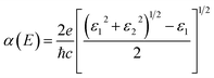 | (7) |
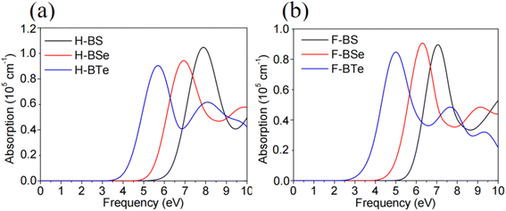 |
| | Fig. 8 (a) and (b) Optical absorption spectra of the monolayers H–BX and F–BX (X = S, Se, and Te), respectively. | |
Studying the optical absorption of H– and F–BO makes little sense due to their insulating characteristics. As a result, we only examine the optical absorption spectra of the monolayers H– and F–BX (X = S, Se, and Te) in this research. The optical absorption spectra of the monolayers H–BX and F–BX (X = S, Se, and Te) are shown in Fig. 8(a) and (b), respectively. Fig. 8 shows that the optical absorption zones of the monolayers H–BX (X = S, Se, and Te) and F–BX (X = S and Se) exhibit considerable optical absorption in the high-frequency ultraviolet range. It follows that the monolayers H–BX (X = S, Se, and Te) and F–BX (X = S and Se) might play a significant role in the development of UV light-emitting diodes (LEDs), high-frequency, high-temperature, and high-power electronic devices, and UV photocatalysts. By combining its band edge state with the fact that F–BTe exhibits apparent optical absorption in the visible-light region, the monolayer can be employed as a photocatalyst in visible-light water splitting, as shown in Fig. 8(b).
4. Conclusion
In summary, using first-principles calculations, we have studied the monolayers H– and F–BX (X = O, S, Se, and Te). The conclusions are as follows: first, the calculation of the binding energies and phonon spectra of the monolayers H– and F–BX indicate that the monolayers H– and F–BX have both highly stable energies and dynamics.
Second, upon studying their electronic properties, we find that H–BO and F–BO are insulators, while H–BS, H–BSe, F–BS, and F–BSe are indirect, ultrawide bandgap semiconductors.
Additionally, H–BTe and F–BTe are indirect semiconductors with broad bandgaps that fulfill the demands of photocatalysts for water splitting. Our research also reveals that F–BTe is a potential candidate for visible-light photocatalytic water splitting because of its excellent photocatalytic qualities, which include high light harvesting capacity, internal electric field, and desirable STH efficiency.
Our work verifies the beneficial effects of surface hydrogenation and fluorination in adjusting the characteristics of 2D materials and also introduces eight new monolayers for use in ultrawide bandgap technology and photocatalytic water splitting.
Conflicts of interest
There are no conflicts to declare.
Acknowledgements
This work is supported by the National Natural Science Foundation of China (Grant No. 12204195 and 52071156), the Fujian Province Department of Science and Technology (China) (Grant No. 2020J05147), and the Scientific Research StartingFoundation of Jimei University (China) (Grant No. ZQ2019015).
References
- K. S. Novoselov, A. K. Geim, S. V. Morozov, D. Jiang, Y. Zhang, S. V. Dubonos, I. V. Grigorieva and A. A. Firsov, Electric Field Effect in Atomically Thin Carbon Films, Science, 2004, 306, 666 CrossRef CAS PubMed.
- A. K. Geim and K. S. Novoselov, The Rise of Graphene, Nat. Mater., 2007, 6, 183 CrossRef CAS PubMed.
- A. H. Castro Neto, F. Guinea, N. M. R. Peres, K. S. Novoselov and A. K. Geim, The Electronic Properties of Graphene, Rev. Mod. Phys., 2009, 81, 109 CrossRef CAS.
- L. Li, Y. Yu, G. J. Ye, Q. Ge, X. Ou, H. Wu, D. Feng, X. H. Chen and Y. Zhang, Black Phosphorus Field-Effect Transistors, Nat. Nanotechnol., 2014, 9, 372 CrossRef CAS PubMed.
- M. Buscema, D. J. Groenendijk, S. I. Blanter, G. A. Steele, H. S. J. van der Zant and A. Castellanos-Gomez, Fast and Broadband Photoresponse of Few-Layer Black Phosphorus Field-Effect Transistors, Nano Lett., 2014, 14, 3347 CrossRef CAS PubMed.
- J. Qiao, X. Kong, Z.-X. Hu, F. Yang and W. Ji, High-Mobility Transport Anisotropy and Linear Dichroism in Few-Layer Black Phosphorus, Nat. Commun., 2014, 5, 4475 CrossRef CAS PubMed.
- V. Tran, R. Soklaski, Y. Liang and L. Yang, Layer-Controlled Bandgap and Anisotropic Excitons in Few-Layer Black Phosphorus, Phys. Rev. B: Condens. Matter Mater. Phys., 2014, 89, 235319 CrossRef.
- H. Liu, A. T. Neal, Z. Zhu, Z. Luo, X. Xu, D. Tománek and P. D. Ye, Phosphorene: An Unexplored 2D Semiconductor with a High Hole Mobility, ACS Nano, 2014, 8, 4033 CrossRef CAS PubMed.
- B. Anasori, M. R. Lukatskaya and Y. Gogotsi, 2D Metal Carbides and Nitrides (MXenes) for Energy Storage, Nat. Rev. Mater., 2017, 2, 16098 CrossRef CAS.
- M. Naguib, V. N. Mochalin, M. W. Barsoum and Y. Gogotsi, 25th Anniversary Article: MXenes: A New Family of Two-Dimensional Materials, Adv. Mater., 2014, 26, 992 CrossRef CAS PubMed.
- F. Shahzad, M. Alhabeb, C. B. Hatter, B. Anasori, S. Man Hong, C. M. Koo and Y. Gogotsi, Electromagnetic Interference Shielding with 2D Transition Metal Carbides (MXenes), Science, 2016, 353, 1137 CrossRef CAS PubMed.
- S. Manzeli, D. Ovchinnikov, D. Pasquier, O. V. Yazyev and A. Kis, 2D Transition Metal Dichalcogenides, Nat. Rev. Mater., 2017, 2, 17033 CrossRef CAS.
- Q. H. Wang, K. Kalantar-Zadeh, A. Kis, J. N. Coleman and M. S. Strano, Electronics and Optoelectronics of Two-Dimensional Transition Metal Dichalcogenides, Nat. Nanotechnol., 2012, 7, 699 CrossRef CAS PubMed.
- M.-Y. Li, et al., Epitaxial Growth of a Monolayer WSe2 -MoS2 Lateral p-n Junction with an Atomically Sharp Interface, Science, 2015, 349, 524 CrossRef CAS PubMed.
- S. Chuang, et al., MoS 2 P-Type Transistors and Diodes Enabled by High Work Function MoO x Contacts, Nano Lett., 2014, 14, 1337 CrossRef CAS PubMed.
- F. Xia, H. Wang and Y. Jia, Rediscovering Black Phosphorus as an Anisotropic Layered Material for Optoelectronics and Electronics, Nat. Commun., 2014, 5, 4458 CrossRef CAS PubMed.
- A. Kormányos, V. Zólyomi, N. D. Drummond and G. Burkard, Spin-Orbit Coupling, Quantum Dots, and Qubits in Monolayer Transition Metal Dichalcogenides, Phys. Rev. X, 2014, 4, 011034 Search PubMed.
- L. Britnell, et al., Strong Light-Matter Interactions in Heterostructures of Atomically Thin Films, Science, 2013, 340, 1311 CrossRef CAS PubMed.
- Z. Hu, Z. Wu, C. Han, J. He, Z. Ni and W. Chen, Two-Dimensional Transition Metal Dichalcogenides:
Interface and Defect Engineering, Chem. Soc. Rev., 2018, 47, 3100 RSC.
- A. Fleurence, R. Friedlein, T. Ozaki, H. Kawai, Y. Wang and Y. Yamada-Takamura, Experimental Evidence for Epitaxial Silicene on Diboride Thin Films, Phys. Rev. Lett., 2012, 108, 245501 CrossRef PubMed.
- L. Tao, E. Cinquanta, D. Chiappe, C. Grazianetti, M. Fanciulli, M. Dubey, A. Molle and D. Akinwande, Silicene Field-Effect Transistors Operating at Room Temperature, Nat. Nanotechnol., 2015, 10, 227 CrossRef CAS PubMed.
- P. Vogt, P. De Padova, C. Quaresima, J. Avila, E. Frantzeskakis, M. C. Asensio, A. Resta, B. Ealet and G. Le Lay, Silicene: Compelling Experimental Evidence for Graphenelike Two-Dimensional Silicon, Phys. Rev. Lett., 2012, 108, 155501 CrossRef PubMed.
- Z. Ni, Q. Liu, K. Tang, J. Zheng, J. Zhou, R. Qin, Z. Gao, D. Yu and J. Lu, Tunable Bandgap in Silicene and Germanene, Nano Lett., 2012, 12, 113 CrossRef CAS PubMed.
- B. Radisavljevic and A. Kis, Mobility Engineering and a Metal–Insulator Transition in Monolayer MoS2, Nat. Mater., 2013, 12, 815 CrossRef CAS PubMed.
- J. R. Schaibley, H. Yu, G. Clark, P. Rivera, J. S. Ross, K. L. Seyler, W. Yao and X. Xu, Valleytronics in 2D Materials, Nat. Rev. Mater., 2016, 1, 16055 CrossRef CAS.
- K. S. Novoselov, A. Mishchenko, A. Carvalho and A. H. Castro Neto, 2D Materials and van Der Waals Heterostructures, Science, 2016, 353, aac9439 CrossRef CAS PubMed.
- G. Fiori, F. Bonaccorso, G. Iannaccone, T. Palacios, D. Neumaier, A. Seabaugh, S. K. Banerjee and L. Colombo, Electronics Based on Two-Dimensional Materials, Nat. Nanotechnol., 2014, 9, 768 CrossRef CAS PubMed.
- H. Tsai, et al., High-Efficiency Two-Dimensional Ruddlesden–Popper Perovskite Solar Cells, Nature, 2016, 536, 312 CrossRef CAS PubMed.
- M. Z. Rahman, C. W. Kwong, K. Davey and S. Z. Qiao, 2D Phosphorene as a Water Splitting Photocatalyst: Fundamentals to Applications, Energy Environ. Sci., 2016, 9, 709 RSC.
- P. Xia, B. Zhu, B. Cheng, J. Yu and J. Xu, 2D/2D g-C3N4/MnO2 Nanocomposite as a Direct Z-Scheme Photocatalyst for Enhanced Photocatalytic Activity, ACS Sustainable Chem. Eng., 2018, 6, 965 CrossRef CAS.
- X. Li, J. Yu, S. Wageh, A. A. Al-Ghamdi and J. Xie, Graphene in Photocatalysis: A Review, Small, 2016, 12, 6640 CrossRef CAS PubMed.
- B. Luo, G. Liu and L. Wang, Recent Advances in 2D Materials for Photocatalysis, Nanoscale, 2016, 8, 6904 RSC.
- T. Su, Q. Shao, Z. Qin, Z. Guo and Z. Wu, Role of Interfaces in Two-Dimensional Photocatalyst for Water Splitting, ACS Catal., 2018, 8, 2253 CrossRef CAS.
- J. Fu, Q. Xu, J. Low, C. Jiang and J. Yu, Ultrathin 2D/2D WO3/g-C3N4 Step-Scheme H2-Production Photocatalyst, Appl. Catal. B Environ., 2019, 243, 556 CrossRef CAS.
- W.-J. Ong, L.-L. Tan, Y. H. Ng, S.-T. Yong and S.-P. Chai, Graphitic Carbon Nitride (g-C3N4)–Based Photocatalysts for Artificial Photosynthesis and Environmental Remediation: Are We a Step Closer To Achieving Sustainability?, Chem. Rev., 2016, 116, 7159 CrossRef CAS PubMed.
- L. Britnell, et al., Electron Tunneling through Ultrathin Boron Nitride Crystalline Barriers, Nano Lett., 2012, 12, 1707 CrossRef CAS PubMed.
- K. Zhang, Y. Feng, F. Wang, Z. Yang and J. Wang, Two Dimensional Hexagonal Boron Nitride (2D-hBN): Synthesis, Properties and Applications, J. Mater. Chem. C, 2017, 5, 11992 RSC.
- X.-J. Ye, Z.-X. Zhu, L. Meng and C.-S. Liu, Two-Dimensional CaFCl: Ultra-Wide Bandgap, Strong Interlayer Quantum Confinement, and n-Type Doping, Phys. Chem. Chem. Phys., 2020, 22, 17213 RSC.
- S. Zhang, Z. Yan, Y. Li, Z. Chen and H. Zeng, Atomically Thin Arsenene and Antimonene: Semimetal-Semiconductor and Indirect-Direct bandgap Transitions, Angew. Chem., Int. Ed., 2015, 54, 3112 CrossRef CAS PubMed.
- P. Johari and V. B. Shenoy, Tuning the Electronic Properties of Semiconducting Transition Metal Dichalcogenides by Applying Mechanical Strains, ACS Nano, 2012, 6, 5449 CrossRef CAS PubMed.
- T. Yu, C. Wang, X. Yan, G. Yang and U. Schwingenschlögl, Anisotropic Janus SiP 2 Monolayer as a Photocatalyst for Water Splitting, J. Phys. Chem. Lett., 2021, 12, 2464 CrossRef CAS PubMed.
- M. Sun and U. Schwingenschl ogl, B2P6: a two-dimensional anisotropic Janus material with potential in photocatalytic water splitting and metal-ion batteries, Chem. Mater., 2020, 32(11), 4795–4800 CrossRef CAS.
- C.-F. Fu, J. Sun, Q. Luo, X. Li, W. Hu and J. Yang, Intrinsic Electric Fields in Two-Dimensional Materials Boost the Solar-to-Hydrogen Efficiency for Photocatalytic Water Splitting, Nano Lett., 2018, 18, 6312 CrossRef CAS PubMed.
- J. Lin, T. Zhang, B. Zhang and X. Wang, Wide-bandgaps Two Dimensional C3XN (X = N and P) for Metal-Free Photocatalytic Water Splitting, Appl. Surf. Sci., 2021, 542, 148597 CrossRef CAS.
- Y. Li, Y.-L. Li, B. Sa and R. Ahuja, Review of Two-Dimensional Materials for Photocatalytic Water Splitting from a Theoretical Perspective, Catal. Sci. Technol., 2017, 7, 545 RSC.
- J. Lin, B. Zhang and T. Zheng, Half-Hydrogenated Monolayer Group III Monochalcogenides: Wide Direct Bandgaps and Potential Photocatalysts for Water Splitting, J. Phys. Chem. C, 2019, 123, 27697 CrossRef CAS.
- L. Zhang, J. Yu, M. Yang, Q. Xie, H. Peng and Z. Liu, Janus Graphene from Asymmetric Two-Dimensional Chemistry, Nat. Commun., 2013, 4, 1443 CrossRef PubMed.
- A.-Y. Lu, et al., Janus Monolayers of Transition Metal Dichalcogenides, Nat. Nanotechnol., 2017, 12, 744 CrossRef CAS PubMed.
- J. Zhang, S. Jia, I. Kholmanov, L. Dong, D. Er, W. Chen, H. Guo, Z. Jin, V. B. Shenoy, L. Shi and J. Lou, Janus Monolayer Transition-Metal Dichalcogenides, ACS Nano, 2017, 11(8), 8192–8198 CrossRef CAS PubMed.
- Y. Bai, Q. Zhang, N. Xu, K. Deng and E. Kan, The Janus Structures of Group-III Chalcogenide Monolayers as Promising Photocatalysts for Water Splitting, Appl. Surf. Sci., 2019, 478, 522 CrossRef CAS.
- C. Zhu, L. Zhang, B. Jiang, J. Zheng, P. Hu, S. Li, M. Wu and W. Wu, Fabrication of Z-scheme Ag3PO4/MoS2 composites with enhanced photocatalytic activity and stability for organic pollutant degradation, Appl. Surf. Sci., 2016, 377, 99–108 CrossRef CAS.
- S. Wang, X. Yang, X. Zhang, X. Ding, Z. Yang, K. Dai and H. Chen, A plate-on-plate sandwiched Z-scheme heterojunction photocatalyst: biOBr–Bi2MoO6 with enhanced photocatalytic performance, Appl. Surf. Sci., 2017, 391, 194–201 CrossRef CAS.
- S. Kwon, J.-H. Ko, K.-J. Jeon, Y.-H. Kim and J. Y. Park, Enhanced Nanoscale Friction on Fluorinated Graphene, Nano Lett., 2012, 12, 6043 CrossRef CAS PubMed.
- F. Withers, M. Dubois and A. K. Savchenko, Electron Properties of Fluorinated Single-Layer Graphene Transistors, Phys. Rev. B: Condens. Matter Mater. Phys., 2010, 82, 073403 CrossRef.
- M. Batzill, The Surface Science of Graphene: Metal Interfaces, CVD Synthesis, Nanoribbons, Chemical Modifications, and Defects, Surf. Sci. Rep., 2012, 67, 83 CrossRef CAS.
- S.-H. Cheng, K. Zou, F. Okino, H. R. Gutierrez, A. Gupta, N. Shen, P. C. Eklund, J. O. Sofo and J. Zhu, Reversible Fluorination of Graphene: Evidence of a Two-Dimensional Wide Bandgap Semiconductor, Phys. Rev. B: Condens. Matter Mater. Phys., 2010, 81, 205435 CrossRef.
- Y. Xu, S. Qi and W. Mi, Electronic Structure and Magnetic Properties of Two-Dimensional h–BN/Janus 2H-VSeX (X = S, Te) van Der Waals Heterostructures, Appl. Surf. Sci., 2021, 537, 147898 CrossRef CAS.
- G. Kresse and J. Furthmȕller, Efficient iterative schemes for ab initio total-energy calculations using a plane-wave basis set, Phys. Rev. B: Condens. Matter Mater. Phys., 1996, 54, 11169–11186 CrossRef CAS PubMed.
- G. Kresse and D. Joubert, From Ultrasoft Pseudopotentials to the Projector Augmented-Wave Method, Phys. Rev. B: Condens. Matter Mater. Phys., 1999, 59, 1758 CrossRef CAS.
- J. P. Perdew, K. Burke and M. Ernzerhof, Generalized Gradient Approximation Made Simple, Phys. Rev. Lett., 1996, 77, 3865–3868 CrossRef CAS PubMed.
- H. J. Monkhorst and J. D. Pack, Special Points for Brillouin-Zone Integrations, Phys. Rev. B: Condens. Matter Mater. Phys., 1977, 16(4), 1748–1749 CrossRef.
- J. Heyd, G. E. Scuseria and M. Ernzerhof, Hybrid Functionals Based on a Screened Coulomb Potential, J. Chem. Phys., 2003, 118, 8207–8215 CrossRef CAS.
- M. D. Segall, P. J. D. Lindan, M. J. Probert, C. J. Pickard, P. J. Hasnip, S. J. Clark and M. C. Payne, First-principles simulation: ideas, illustrations and the CASTEP code, J. Phys.: Condens. Matter, 2002, 14, 2717–2744 CrossRef CAS.
- S. Baroni, S. de Gironcoli, A. dal Corso and P. Giannozzi, Phonons and related crystal properties of extended systems from density-functional perturbation theory, Rev. Mod. Phys., 2001, 73, 515–562 CrossRef CAS.
- X. Li, Z. Li and J. Yang, Proposed Photosynthesis Method for Producing Hydrogen from Dissociated Water Molecules Using Incident Near-Infrared Light, Phys. Rev. Lett., 2014, 112, 018301 CrossRef PubMed.
- C. Fu, J. Sun, Q. Luo, X. Li, W. Hu and J. Yang, Intrinsic electric fields in twodimensional materials boost the solar-to-hydrogen efficiency for photocatalytic water splitting, Nano Lett., 2018, 18(10), 6312–6317 CrossRef CAS PubMed.
- B. Mortazavi and T. Rabczuk, Boron Monochalcogenides; Stable and Strong Two-Dimensional Wide Band-Gap Semiconductors, Energies, 2018, 11, 1573 CrossRef.
- P. Mishra, D. Singh, Y. Sonvane and R. Ahuja, Two-dimensional boron monochalcogenide monolayer for thermoelectric material, Sustain. Energy Fuels, 2020, 4, 2363–2369 RSC.
|
| This journal is © The Royal Society of Chemistry 2023 |
Click here to see how this site uses Cookies. View our privacy policy here. 
 Open Access Article
 This Open Access Article is licensed under a Creative Commons Attribution-Non Commercial 3.0 Unported Licence
 a,
Bofeng Zhang*b and
Jiahe Lin
a,
Bofeng Zhang*b and
Jiahe Lin